EP4105642A1 - Optisches abbildungssystem und system zur detektion von biochemischen substanzen damit - Google Patents
Optisches abbildungssystem und system zur detektion von biochemischen substanzen damit Download PDFInfo
- Publication number
- EP4105642A1 EP4105642A1 EP20919158.4A EP20919158A EP4105642A1 EP 4105642 A1 EP4105642 A1 EP 4105642A1 EP 20919158 A EP20919158 A EP 20919158A EP 4105642 A1 EP4105642 A1 EP 4105642A1
- Authority
- EP
- European Patent Office
- Prior art keywords
- lenses
- group
- optical imaging
- imaging system
- objective lens
- Prior art date
- Legal status (The legal status is an assumption and is not a legal conclusion. Google has not performed a legal analysis and makes no representation as to the accuracy of the status listed.)
- Pending
Links
Images











Classifications
-
- G—PHYSICS
- G02—OPTICS
- G02B—OPTICAL ELEMENTS, SYSTEMS OR APPARATUS
- G02B21/00—Microscopes
- G02B21/02—Objectives
-
- G—PHYSICS
- G01—MEASURING; TESTING
- G01N—INVESTIGATING OR ANALYSING MATERIALS BY DETERMINING THEIR CHEMICAL OR PHYSICAL PROPERTIES
- G01N21/00—Investigating or analysing materials by the use of optical means, i.e. using sub-millimetre waves, infrared, visible or ultraviolet light
- G01N21/62—Systems in which the material investigated is excited whereby it emits light or causes a change in wavelength of the incident light
- G01N21/63—Systems in which the material investigated is excited whereby it emits light or causes a change in wavelength of the incident light optically excited
- G01N21/64—Fluorescence; Phosphorescence
- G01N21/645—Specially adapted constructive features of fluorimeters
- G01N21/6456—Spatial resolved fluorescence measurements; Imaging
-
- G—PHYSICS
- G01—MEASURING; TESTING
- G01N—INVESTIGATING OR ANALYSING MATERIALS BY DETERMINING THEIR CHEMICAL OR PHYSICAL PROPERTIES
- G01N21/00—Investigating or analysing materials by the use of optical means, i.e. using sub-millimetre waves, infrared, visible or ultraviolet light
- G01N21/62—Systems in which the material investigated is excited whereby it emits light or causes a change in wavelength of the incident light
- G01N21/63—Systems in which the material investigated is excited whereby it emits light or causes a change in wavelength of the incident light optically excited
- G01N21/64—Fluorescence; Phosphorescence
- G01N21/645—Specially adapted constructive features of fluorimeters
-
- G—PHYSICS
- G02—OPTICS
- G02B—OPTICAL ELEMENTS, SYSTEMS OR APPARATUS
- G02B21/00—Microscopes
- G02B21/0004—Microscopes specially adapted for specific applications
- G02B21/002—Scanning microscopes
- G02B21/0024—Confocal scanning microscopes (CSOMs) or confocal "macroscopes"; Accessories which are not restricted to use with CSOMs, e.g. sample holders
- G02B21/0052—Optical details of the image generation
- G02B21/0076—Optical details of the image generation arrangements using fluorescence or luminescence
-
- G—PHYSICS
- G02—OPTICS
- G02B—OPTICAL ELEMENTS, SYSTEMS OR APPARATUS
- G02B21/00—Microscopes
- G02B21/36—Microscopes arranged for photographic purposes or projection purposes or digital imaging or video purposes including associated control and data processing arrangements
- G02B21/365—Control or image processing arrangements for digital or video microscopes
- G02B21/367—Control or image processing arrangements for digital or video microscopes providing an output produced by processing a plurality of individual source images, e.g. image tiling, montage, composite images, depth sectioning, image comparison
-
- G—PHYSICS
- G02—OPTICS
- G02B—OPTICAL ELEMENTS, SYSTEMS OR APPARATUS
- G02B27/00—Optical systems or apparatus not provided for by any of the groups G02B1/00 - G02B26/00, G02B30/00
- G02B27/0025—Optical systems or apparatus not provided for by any of the groups G02B1/00 - G02B26/00, G02B30/00 for optical correction, e.g. distorsion, aberration
-
- G—PHYSICS
- G01—MEASURING; TESTING
- G01N—INVESTIGATING OR ANALYSING MATERIALS BY DETERMINING THEIR CHEMICAL OR PHYSICAL PROPERTIES
- G01N21/00—Investigating or analysing materials by the use of optical means, i.e. using sub-millimetre waves, infrared, visible or ultraviolet light
- G01N21/62—Systems in which the material investigated is excited whereby it emits light or causes a change in wavelength of the incident light
- G01N21/63—Systems in which the material investigated is excited whereby it emits light or causes a change in wavelength of the incident light optically excited
- G01N21/64—Fluorescence; Phosphorescence
- G01N2021/6417—Spectrofluorimetric devices
- G01N2021/6421—Measuring at two or more wavelengths
-
- G—PHYSICS
- G01—MEASURING; TESTING
- G01N—INVESTIGATING OR ANALYSING MATERIALS BY DETERMINING THEIR CHEMICAL OR PHYSICAL PROPERTIES
- G01N21/00—Investigating or analysing materials by the use of optical means, i.e. using sub-millimetre waves, infrared, visible or ultraviolet light
- G01N21/62—Systems in which the material investigated is excited whereby it emits light or causes a change in wavelength of the incident light
- G01N21/63—Systems in which the material investigated is excited whereby it emits light or causes a change in wavelength of the incident light optically excited
- G01N21/64—Fluorescence; Phosphorescence
- G01N21/645—Specially adapted constructive features of fluorimeters
- G01N2021/6463—Optics
- G01N2021/6478—Special lenses
-
- G—PHYSICS
- G01—MEASURING; TESTING
- G01N—INVESTIGATING OR ANALYSING MATERIALS BY DETERMINING THEIR CHEMICAL OR PHYSICAL PROPERTIES
- G01N21/00—Investigating or analysing materials by the use of optical means, i.e. using sub-millimetre waves, infrared, visible or ultraviolet light
- G01N21/62—Systems in which the material investigated is excited whereby it emits light or causes a change in wavelength of the incident light
- G01N21/63—Systems in which the material investigated is excited whereby it emits light or causes a change in wavelength of the incident light optically excited
- G01N21/64—Fluorescence; Phosphorescence
- G01N21/645—Specially adapted constructive features of fluorimeters
- G01N21/6456—Spatial resolved fluorescence measurements; Imaging
- G01N21/6458—Fluorescence microscopy
Definitions
- the subject matter relates to field of detection, and more particularly, to an optical imaging system and a biochemical substance detection system using the optical imaging system.
- An optical imaging system of an imaging analysis instrument used in the field of biochemical substance analysis, such as a gene sequencer is mostly designed based on a scientific area-array camera with high sensitivity. Since an area of an area to be measured of a sequencing chip is usually much larger than a single visible area of objective lens of the optical imaging system, it is necessary to use a manner of sequential scanning of multiple rows or columns to complete the photographing of areas to be detected of the entire sequencing chip. Splicing will be carried out in a data analysis stage.
- a common scientific area-array camera usually uses a design scheme based on platform stepping when performing sequential scanning of multiple rows or columns.
- the platform is equipped with the sequencing chip and is moved to meet needs of taking photos at different positions.
- the platform moves to a photographing location, the platform needs to slow down to a standstill before taking photos, otherwise a smear occurs in a photographed image.
- the platform must have the accelerate and decelerate ability to stop quickly from a high speed and resume moving at a high speed from a stationary state after taking photos.
- the acceleration and deceleration of the platform take considerable time, and this presents one of the bottlenecks to high-throughput optical sequencing.
- the existing microscope objective usually cannot have both large field of view and large numerical aperture, so it is not suitable for high-throughput optical imaging system.
- an optical imaging system and a biochemical substance detection system using the optical imaging system are needed.
- a first aspect provides an optical imaging system configured for photographing a sample.
- the optical imaging system includes a lighting module and an imaging module.
- the lighting module is configured for outputting excitation light, the excitation light is configured to excite the sample to generate excited light.
- the imaging module includes a time delay integration line scan camera, the time delay line scan camera is configured to record the excited light.
- a second aspect provides a biochemical substance detection system including the above optical imaging system.
- the optical imaging system provided and the biochemical substance detection system applying the optical imaging system in the embodiment of the disclosure achieve beneficial effects as follows: first, the industrial or scientific TDI camera is adopted to collect the excited light, which reduces the photographing time of each sample and improves the detection flux. Second, on the one hand, the excited light can be divided into multiple channels for imaging using the light filtering system composed of the light splitting device and the light filtering device, on the other hand, the interference of excitation light and other light, such as detection light, on the imaging of excited light is prevented, and the imaging quality is improved.
- the output end face of the light source is a rectangle, or further a slender rectangle, and the excitation light output from the light source is shaped into an illumination spot suitable for the photosensitive surface of the TDI camera by the excitation light shaping unit, utilizing the light source energy to a large extent and improving the uniformity of the illumination spot.
- the objective lens with special structure is adopted to enable a large field of view and a large numerical aperture, distortion and flat field achromatism being thereby reduced.
- a focusing system is adopted, and the focusing system adjusts the distance between the objective lens and the sample carrier in real time, so that the sample carrier is kept on the focal plane of the objective lens, compensating for the change of distance between the sample carrier and the objective lens caused by a change of environmental temperature, mechanical vibration, sample flexing or other reasons, ensuring the imaging quality.
- the focusing system adopts a specific method to calculate the distance between the sample carrier and the objective lens, which effectively eliminates the influence on the detection results of signal noise and a change of brightness of the detection light.
- Optical imaging system 1 lighting module 11; focusing module 13; imaging module 15; objective lens 16; light source 111, 1301; excitation light shaping unit 113; sample carrier 2; TDI camera 151; tube lens 152, 1303; cut-off filter 153, 116; light splitting device 154; dichroic mirror A, B, C, D, E; plane mirror 115; photographing time t1, t2; first group of lenses 161; second group of lenses 162; third group of lenses 163; fourth group of lenses 164; fifth group of lenses 165; sixth group of lenses 166; seventh group of lenses 167; first lens L1; second lens L2; third lens L3; fourth lens L4; fifth lens L5; sixth lens L6; seventh lens L7; eighth lens L8; ninth lens L9; tenth lens L10; eleventh lens L11; twelve lens L12; thirteen lens L13; fourteen L14; multimode fiber 1111; output end face 1112; first shaping unit 113a; second shaping unit 113b; cylindrical lens C1,
- FIG. 1 is a schematic diagram of an optical imaging system according to an embodiment of the present disclosure.
- the optical imaging system 1 includes a lighting module 11, a focusing module 13, and an imaging module 15.
- the imaging module 15 uses a time delay integration (TDI) line scan camera (hereinafter referred to as TDI camera) for imaging. Furthermore, the TDI camera is an industrial or scientific TDI camera.
- the lighting module 11, the focusing module 13, and the imaging module 15 share some light path guiding components and an objective lens 16.
- the lighting module 11 includes a light source 111 and an excitation shaping unit 113. Excitation light emitted by the light source 111 is shaped into linear light spot adapted to a photosensitive surface of the TDI camera by the excitation shaping unit 113.
- the linear light spot is guided to the objective lens 16 through light path guiding elements and is emitted to a sample carried on the sample carrier 2 through the objective lens 16.
- the sample is excited by the excitation light to generate excited light, the excited light enters the imaging module 15 through the objective lens and is recorded by the TDI camera in the imaging module 15.
- the focusing module 13 emits detection light, the detection light is guided into the objective lens 16 by the light path guiding components, and then emitted to the sample carrier 2 through the objective lens 16.
- the detection light will not excite the sample to generate the excited light, but will be reflected back into the objective lens 16 by the sample carrier 2.
- the detection light is guided into the focusing module 13 through the objective lens 16 and the light path guiding components.
- the focusing module 13 analyzes and determines a positional relationship between the sample carrier 2 and the objective lens 16 and adjusts a position of the objective lens 16 relative to the sample carrier 2 according to the determined positional relationship between the sample carrier 2 and the objective lens 16, so that the sample carrier 2 is always located on a focal plane of the objective lens 16.
- the light source 111 is a laser light source, and the excitation light is laser light.
- the optical imaging system 1 is a sequencing photography system, which is configured to take photos of DNA samples to analyze base sequences of DNA samples.
- the DNA samples are carried on the sample carrier 2.
- Four types of bases A, T, G, and C of the DNA sample are labeled with different fluorescent dyes respectively.
- the laser light emitted from the objective lens 16 excites the DNA samples to emit four kinds of fluorescence of different wavelengths.
- the imaging module 15 includes four TDI cameras 151.
- the arrangement of the four TDI cameras 151 gives the optical imaging system 1 four imaging channels.
- a tube lens 152 and a cut-off filter 153 are arranged in front of each TDI camera 151.
- Each cut-off filter 153 only allows fluorescence in one wavelength range to enter a corresponding TDI camera 151, so that the corresponding TDI camera 151 records only a fluorescence signal emitted by one type of the bases A, T, G, and C.
- the imaging module 15 also includes a plurality of light splitting devices 154.
- the light splitting devices 154 guide light of different wavelengths into different imaging channels by reflecting the light of one wavelength range and transmitting the light of another wavelength range, so that the light of different wavelengths is recorded by different TDI cameras 151.
- the light splitting devices 154 are dichroic mirrors
- the imaging module 15 includes dichroic mirrors A, B, C, and D.
- the dichroic mirror A is arranged to correspond to the objective lens 16, and forms an angle of 45 ° with an optical axis of the objective lens 16, and is configured to transmit the excited light and reflect excitation light and detection light.
- the dichroic mirror B is arranged at a rear side of the dichroic mirror A, is arranged in parallel with the dichroic mirror A, and is configured to guide the excited light of different wavelengths to the dichroic mirrors C and D through transmission and reflection.
- the dichroic mirrors C and D then guide the excited light with different wavelengths to different cut-off filters 153 through transmission and reflection, then the excited light enters the corresponding TDI camera 151 through the tube lens 152.
- the lighting module 11 and the focusing module 13 share the dichroic mirror A of the imaging module 15.
- the lighting module 11 and the focusing module 13 also share a dichroic mirror E.
- the dichroic mirror E guides the excitation light and detection light incident from different angles to the dichroic mirror A, then the excitation light and detection light is guided into the objective lens 16 by the dichroic mirror A.
- the lighting module 11 also includes a plane mirror 115, the plane mirror 115 reflects the excitation light shaped by the excitation light shaping unit 113 to the dichroic mirror E.
- the TDI camera 151 is used. Multiple rows of pixels of a photosensitive chip of the TDI camera 151 can perform charge transfer row by row to image the same target for multiple exposures. By synchronizing the TDI camera 151 with the sample carrier 2, photographing time of each sample can be significantly reduced, and detection flux can be improved.
- FIG. 2 shows photographing time per row as a comparation between the TDI camera 151 and the traditional area-array camera.
- T1 represents the photographing time for each row of the TDI camera 151
- T2 represents the photographing time for each row of the traditional area-array camera.
- a detection platform carrying the sample carrier 2 can be controlled to move at a constant speed, so that the TDI camera 151 can continuously scan the same row of the sample to collect image information of such row.
- the detection platform with the TDI camera 151 only needs to be driven to accelerate or decelerate once when the row is changed, which improves time utilization of the optical imaging system 1, improves the detection flux of the biochemical substance detection device applying the optical imaging system 1, and avoids risks caused by frequent acceleration or deceleration of the detection platform.
- the objective lens 16 homogenizes and transmits rectangular line spot from the lighting module 11 to the sample carrier 2, and also guides the detection light from the focusing module 13 to the sample carrier 2.
- the objective lens 16 collects the excited light, the collected excited light passes through the tube lens 152, so as to obtain DNA fluorescence images of each channel on each TDI camera 151.
- a numerical aperture NA of the objective lens 16 is required to be greater than 0.8 according to Rayleigh Criterion.
- an effective field of view for imaging is a narrow rectangular region with a large length-width ratio, so that the TDI camera 151 needs a large linear field of view for imaging.
- an object diameter field of view of the objective lens 16 is required to be more than 1.5mm.
- the objective lens 16 needs to have a large numerical aperture and a large field of view at the same time.
- the low magnification objective lens usually has a large field of view but a small numerical aperture
- the high magnification objective lens has a large numerical aperture but a small field of view; generally, the product of the two is less than 0.8, so ultra-high throughput is difficult to achieve.
- the objective lens 16 provided by the embodiment is to meet the following specifications:
- the numerical aperture NA is greater than or equal to 0.7, an effective working distance is greater than 1.2mm, a focal length is greater than 2.5mm, an apochromatic aberration of 500nm to 800nm wavelength light wave is less than 0.4um; a field curve is less than 0.4um, an object field of view is greater than ⁇ 1.2mm, and a distortion when combined with the tube lens is less than 1%.
- the objective lens 16 provided in the embodiment is a flat-field achromatic objective lens with large field of view, large numerical aperture, and small distortion, and is suitable for a 0.25mm cover glass and a 0.05mm water layer.
- FIG. 3 is a schematic diagram of the objective lens 16 according to the embodiment.
- the objective lens 16 includes seven groups of lenses 161 to 167.
- First group of lenses 161 to seventh group 167 are arranged successively from an object side to an image side, in which the first three groups of lenses 161 to 163 bear a negative power, and the last four groups of lenses 164 to 167 bear a positive power.
- the first group of lenses 161 includes a first lens L1, which is a thick meniscus lens with a positive power, forming an aplanatic lens and generating a positive field curvature.
- a second group of lenses 162 includes a second lens L2, which is a crescent lens with a positive power and bears a positive deflection angle with the first lens L1.
- a third group of lenses 163 includes a third lens L3, a fourth lens L4, and a fifth lens L5.
- the third lens L3, the fourth lens L4, and the fifth lens L5 are glued together successively to form a triple cemented lens group with a positive power, which is mainly configured to correct comatic aberration and chromatic aberration.
- a fourth group of lenses 164 includes a sixth lens L6, which is a thin crescent lens with a positive power.
- a fifth group of lenses 165 includes a seventh lens L7 and an eighth lens L8. The seventh lens L7 and the eighth lens L8 are glued together to form a double cemented lens group with a positive power.
- a sixth group of lenses 166 includes a ninth lens L9 and a tenth lens L10.
- the ninth lens L9 and the tenth lens L10 are glued together to form a double cemented lens group with a negative power.
- the seventh group of lenses 167 includes an eleventh lens L11 and a twelfth lens L12.
- the eleventh lens L11 and the twelfth lens L12 are glued together to form a double cemented meniscus-negative lens group with a negative power.
- the sixth group of lenses 166 and the seventh group of lenses 167 are configured to control a field curvature and distortion.
- thicknesses of the thick meniscus lens, the meniscus lens, and the thin meniscus lens along an optical axis decrease successively. That is, a thickness of the thick meniscus lens along the optical axis is greater than that of the meniscus lens, and a thickness of the meniscus lens along the optical axis is greater than that of the thin meniscus lens.
- the terms "thick” and “thin” in the embodiment are relative and are only used for a description of a thickness of an object.
- f1 is a focal length of the first group of lenses 161
- f2 is a focal length of the second group of lenses 162
- f3 is a focal length of the third group of lenses 163
- f4 is a focal length of the fourth group of lenses 164
- f5 is a focal length of the fifth group of lenses 165
- f6 is a focal length of the sixth group of lenses 166
- f7 is a focal length of the seventh group of lenses 167
- fobj is a focal length of the objective lens 16.
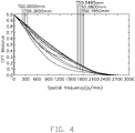
- FIG. 4 shows a full field and full band MTF (Modulation Transfer Function) curve of the objective lens 16
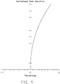
- FIG. 5 shows a distortion curve of the objective lens 16 obtained by simulation
- FIG. 6 shows an envelope energy diagram of the objective lens 16 obtained by simulation. From the above simulation results, it can be seen that the objective lens 16 is close to the diffraction limit in imaging results, and its normalized field distortion is less than 1% with high resolution.
- MTF Modulation Transfer Function
- FIG. 7 is a schematic diagram of a combination of the objective lens 16 and the tube lens 152 according to the embodiment.
- the tube lens 152 includes four lenses, which are glued together to form two double cemented lenses, hereinafter referred to as a thirteenth lens L13 and a fourteenth lens L14.
- a focal length of the tube lens 152 is 150mm to 250mm.
- a specific focal length value of the tube lens 152 is set according to the focal length of the objective lens 16, a pixel size and number of the TDI camera 151, and the magnification and resolution required by the optical imaging system 1.
- the combination of the tube lens 152 and the objective lens 16 needs to meet imaging restrictions such as distortion and a field curvature, and the tube lens 152 compensates for the residual aberration of the objective lens 16.
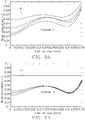
- FIGS. 8A to 8D are wavefront aberration curves of the combination of the objective lens 16 and the tube lens 152 obtained by simulation in imaging channels 1 to 4, and FIG 9 is a distortion curve of the combination of the objective lens 16 and the tube lens 152 obtained by simulation.
- a horizontal line H in FIGS. 8A to 8D represents the diffraction limit.
- the wave aberration of the combination of the objective lens 16 and the tube lens 152 in imaging channels 1 to 4 is lower than the horizontal line H, which proves that the combination of the objective lens 16 and the tube lens 152 has reached the limit of resolution requirements.
- the normalized field distortion of the combination of the objective lens 16 and the tube lens 152 is less than 1%.
- the objective lens 16 is an infinity correction objective lens, and the objective lens 16 changes the received excited light emitted by the sample into a parallel light or similar parallel light. In this way, it is convenient to add a light splitting device 154 between the objective lens 16 and the tube lens 152 as needed.
- FIG. 10 is a schematic diagram of an output end face of the light source 111 of the embodiment.
- the light source 111 is a laser light source that emits red and green laser light.
- the light source includes an optical fiber coupler (not shown) and a multimode optical fiber 1111.
- the red and green laser light is coupled to the multimode fiber 1111 through the fiber coupler for output.
- the multimode fiber 1111 has an output end face 1112, which is the output end face of the light source 111.
- the output end face 1112 is rectangular to match a long strip-shaped photosensitive surface of the TDI camera 151.
- the rectangular output end face of the light source 111 can be adapted to the TDI camera 151, which can improve the utilization of excitation light.
- FIG. 11 is a schematic diagram of a combination of an excitation light shaping unit 113 and the objective lens 16 according to an embodiment.
- the excitation light shaping unit 113 includes a first shaping unit 113a and a second shaping unit 113b.
- the first shaping unit 113a and the second shaping unit 113b are arranged successively from the image side to the object side.
- the first shaping unit 113a is configured to shape rectangular light spot emitted by the light source 111 in a first direction
- the second shaping unit 113b is configured to shape an illumination spot emitted by the light source 111 in a second direction, the first direction and the second direction being perpendicular to each other.
- the first shaping unit 113a and the second shaping unit 113b are cylindrical lenses C1 and C2 respectively.
- the cylindrical lens C1 enlarges the illumination spot in the X direction shown in FIG. 1
- the cylindrical lens C2 reduces the illumination spot in the Y direction shown in FIG. 1 , so that the illumination spot finally forms the length-width ratio required for an imaging scan of the TDI camera 151.
- the length-width ratio of the illumination spot output by the lighting module 11 can be adjusted.
- the cylindrical lenses C1 and C2 can realize the shaping of the length-width ratio of the illumination spot of 10:1, and multiply the rectangular output end face 1112 of the optical fiber 1111, so that the length-width ratio of the illumination spot output by the lighting module 11 can reach about 20:1.
- two cylindrical lenses C1 and C2 are used to realize the shaping of the illumination spot.
- the excitation shaping unit 113 has a simple structure and is easy to assemble and adjust.
- the deviation of illumination spot caused by the component itself and assembly tolerance can be reduced.
- critical illumination is used to strictly control the linear uniformity of illumination, and uniform illumination is provided for the excited light while maximizing the energy of the light source 111.
- FIG. 12 is a schematic diagram of a combination of an excitation light shaping unit 113 and the objective lens 16 according to another embodiment.
- the first shaping unit 113a and the second shaping unit 113b are cylindrical lenses C3 and C4 respectively.
- the cylindrical lens C3 reduces the illumination spot in the Y direction shown in FIG. 1
- the cylindrical lens C4 enlarges the illumination spot in the X direction shown in FIG. 1 , so that the illumination spot finally forms the length-width ratio required for the imaging scan of the TDI camera 151.
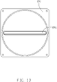
- FIG. 13 is a schematic diagram of a photosensitive surface of the TDI camera 151 in the embodiment.
- the photosensitive surface 1511 of the TDI camera 151 is a rectangular surface, or further a long strip-shaped surface.
- FIG. 14 is an irradiance map of an image plan obtained by simulation. Specifically, FIG 14 shows an irradiance map of an image plan obtained by simulating the optical imaging system 1 with a non-sequential simulation software. In the simulation, an input power of the light source 111 is normalized to 1W, the dichroic mirrors A to E are simplified to beam splitters with a reflection/projection of 50/50, and transmittance of all lenses is assumed to be 100%. It can be seen from the irradiance map of image plan that the uniformity of illuminance of image plane is greater than 85%.
- first shaping unit 113a and the second shaping unit 113b may also be optical wedges, microlenses, diffractive optical elements, etc.
- a cut-off filter 153 is arranged before each barrel mirror 152.
- a cut-off filter 116 is arranged between the light source 111 and the excitation light shaping unit 113 to filter out stray light beyond the excitation wavelength.
- the cut-off filters 153 and 116 and the dichroic mirrors A to E constitute a filter system, so that four kinds of excited light are imaged through four channels and collected by four TDI cameras 151.
- the filter system realizes the division of the excited light into various channels for imaging.
- the filter system also filters the excitation and detection light out of the TDI camera 151.
- the rejection rate of the cut-off filter 153 is 8.
- FIG. 15 is a control schematic diagram of the optical imaging system 1 in the embodiment.
- the optical imaging system 1 also includes a control device 17.
- the control device 17 is configured to control a moving speed of the detection platform (which is the movable platform 17 in the embodiment) to match and keep synchronized with a frequency of the TDI camera 151.
- the control device 17 is also configured to control switch-on of the light source 111 to keep synchronized with the photographing by the TDI camera 151.
- the control device 17 is communicatively coupled to the movable platform 18 on which the sample carrier 2 is placed.
- the control device 17 triggers the light source 111 and the TDI camera 151 at the same time to synchronize in relation to the sample, the light source 111, and the TDI camera 151.
- the frequency of the TDI camera 151 automatically matches the moving speed of the movable platform 18, so that the photographed image is not deformed.
- the movable platform 18 can be controlled to move in the X direction and the Y direction perpendicular to the X direction, and can be controlled to rotate in a plane formed by the X direction and the Y direction, so that the movable platform 18 can be moved or positioned to a preset position.
- the objective lens 16 can be controlled to move in the Z direction shown in the figures.
- the Z direction is perpendicular to both the X direction and the Y direction.
- the focusing module 13 is configured to emit detection light to detect a positional relationship between the sample carrier 2 and the objective lens 16, and is configured to control the objective lens 16 to move in the Z direction according to detection results to adjust a distance between the objective lens 16 and the sample carrier 2, so that the sample carrier 2 is always on the focal plane of the objective lens 16.
- the focusing module 13 can compensate for change of a distance between the objective lens 16 and the sample carrier 2 caused by change of ambient temperature, mechanical vibration, flexing of the sample carrier 2, undulation in surface flatness of the sample carrier 2, or change of thickness of the sample carrier 2.
- FIG. 16 is a schematic diagram showing the focusing module 13 performing focusing in the embodiment.
- the detection light emitted by the focusing module 13 is irradiated to the sample carrier 2 through the objective lens 16, is reflected back to the objective lens 16 by the sample carrier 2, and returns to the focusing module 13 along the same light path through the objective lens 16.
- the focusing module 13 determines whether the sample carrier 2 is located on the focal plane of the objective lens 16 according to the returned detection light.
- the focusing module 13 sends a signal to the drive unit 161 that drives the objective lens 16 to move, and controls the drive unit 161 to drive the objective lens 16 to move closer to or further from the sample carrier 2, so that the sample carrier 2 is again on the focal plane of the objective lens 16.
- imaging data of each TDI camera 151 is transmitted to a computer device 19, the computer device 19 comprehensively evaluates imaging quality of all TDI cameras 151 according to preset rules and determines a standard position of the objective lens 16 (that is, a position of the objective lens 16 in the Z direction when the sample carrier 2 is located on the focal plane of the objective lens 16) based on principle of optimal quality, and obtaining a standard value representing the standard position of the objective lens 16.
- the standard value is supplied to the focusing module 13.
- the focusing module 13 includes a detection light path 130, a sensing unit 131, and a control unit 132.
- the sensing unit 131 senses the returned detection light and outputs an electrical signal.
- the control unit 132 obtains the detection value according to the electrical signal output by the sensing unit 131, compares the detection value with the standard value, and obtains a control signal to control the drive unit 161 to drive the objective lens 16 to move closer to or further from the sample carrier 2.
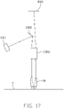
- FIG. 17 is schematic diagram of a light path showing the focusing module 13 performing focusing in the embodiment.
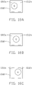
- FIG. 18A to FIG. 18C are schematic diagrams showing the sensing unit 131 of the focusing module 13 sensing whether the sample carrier 2 is in the focal plane of the objective lens 16 in the embodiment.
- the detection light path includes a light source 1301 and a tube lens 1303.
- the sensing unit 131 includes a sensor 1311.
- the detection light emitted by the light source 1301 passes through the tube lens 1303 and the objective lens 16 (in the embodiment, it enters the tube lens 1303 after being reflected by a speculum 1305), is irradiated to the sample carrier 2 and is reflected by the sample carrier 2.
- the reflected detection light is irradiated to the sensor 1311 after passing through the objective lens 16 and the tube lens 1303.
- the sensor 1311 adopts a photoelectric sensor, specifically a PD (Photodiode) sensor 1312.
- the PD sensor 1312 is provided with two sensing areas 1312a and 1312b. Positions of the detection light irradiated to the sensing areas 1312a and 1312b can determine a position between the sample carrier 2 and the objective lens 16.
- a spot G of the detection light is biased towards the sensing area 1312a, which means that the sample carrier 2 is above the focal plane of the objective lens 16.
- FIG. 18A a spot G of the detection light is biased towards the sensing area 1312a, which means that the sample carrier 2 is above the focal plane of the objective lens 16.
- an area of the spot G of the detection light falling on the sensing area 1312a is the same as an area falling on the sensing area 1312b, or the difference between the two is within a preset range, which means that the sample carrier 2 is on the focal plane of the objective lens 16.
- the spot of the detection light is biased towards the sensing area 1312b, which means that the sample carrier 2 is below the focal plane of the objective lens 16.
- the sensing area 1312a converts a received optical signal into an electrical signal PD1 for output
- the sensing area 1312b converts a received optical signal into an electrical signal PD2 for output.
- the control unit 132 determines the defocus direction and defocus amount corresponding to the sample carrier 2 according to the two received electrical signals PD1 and PD2, and then controls the drive unit 161 to drive the objective lens 16 to move closer to or further from the sample carrier 2 by a necessary distance.
- a corresponding control signal DIV for controlling the drive unit 161 is generated by dividing a difference of the electrical signals PD1 and PD2 by their sum.
- signal noise can be effectively filtered out, and the focusing accuracy is thus not influenced by brightness fluctuation of the light source 1301.
- ⁇ is a signal amplification coefficient
- a difference signal DIFF is the difference between PD1 and PD2
- a sum signal SUM is the sum of PD1 and PD2
- ⁇ is a preset voltage offset
- FIG. 19 shows changes of various signals obtained in focusing.
- the abscissa represents a relative millimeter distance between the objective lens 16 and the sample carrier 2 in the Z-axis
- curve O represents the difference signal DIFF
- curve Q represents the sum signal SUM
- curve P represents the control signal DIV
- curve R represents a relative coordinate position between the drive unit 161 and the sample carrier 2 in the Z-direction.
- an intersection point S of curve R and curve P represents the focal plane of the objective lens 16, and the value (DIV value) of curve P at the intersection point S is the standard value representing the standard position of objective lens 16.
- FIG. 20 is a schematic diagram of a biochemical substance detection system according to an embodiment of the present disclosure.
- the biochemical substance detection system 5 includes an optical imaging system 51.
- the optical imaging system 51 can be the optical imaging system 1 described in the above embodiments.
- FIG. 21 is a schematic diagram of the biochemical substance detection system according to another embodiment of the present disclosure.
- the biochemical substance detection system 6 includes an optical imaging system 61 and a detection platform 62.
- the optical imaging system 61 can be the optical imaging system 1 described in the above embodiments, and the detection platform 62 is configured to carry the sample carrier.
- the detection platform 62 is a movable platform, and a control device 611 of the optical imaging system 61 is configured to control and coordinate the optical imaging system 61 and the detection platform 62.
- control device 611 is configured to control the moving speed of the detection platform 62 to match and synchronize with the frequency of the TDI camera 613 of the optical imaging system 61
- control device 63 is also configured to control switch-on of the light source 615 of the optical imaging system 61 to synchronize with the photographing by the TDI camera 613.
- the control device 611 triggers the light source 615 and the TDI camera 613 at the same time to keep the sample (not shown), the light source 615, and the TDI camera 613 carried on the detection platform 62 in synchronization.
- the frequency of the TDI camera 613 automatically matches the moving speed of the detection platform 62, so that the photographed image is not deformed.
- the industrial or scientific TDI camera is adopted to collect the excited light, which reduces the photographing time of each sample and improves the detection flux.
- the excited light can be divided into multiple channels for imaging using the light filtering system composed of the light splitting device and the light filtering device, on the other hand, the interference of excitation light and other light, such as detection light, on the imaging of excited light is prevented, and the imaging quality is improved.
- the output end face of the light source is a rectangle, or further a slender rectangle, and the excitation light output from the light source is shaped into an illumination spot suitable for the photosensitive surface of the TDI camera by the excitation light shaping unit, utilizing the light source energy to a large extent and improving the uniformity of the illumination spot.
- the objective lens with special structure is adopted to enable a large field of view and a large numerical aperture, distortion and flat field achromatism being thereby reduced.
- the focusing system adjusts the distance between the objective lens and the sample carrier in real time, so that the sample carrier is kept on the focal plane of the objective lens, compensating for changes of distance between the sample carrier and the objective lens caused by a change of environmental temperature, mechanical vibration, sample flexing or other reasons, ensuring the imaging quality.
- the focusing system adopts a specific method to calculate the distance between the sample carrier and the objective lens, which effectively eliminates the influence on the detection results of noise and a change of brightness of the detection light source.
- the first shaping unit and the second shaping unit of the excitation shaping unit may not be limited to one lens, but may be composed of multiple lenses; the lens constituting the first shaping unit and the second shaping unit are also not to be limited to cylindrical lens, aspheric lens, spherical lens, or Fresnel lens.
- the number of TDI cameras and corresponding imaging channels is not limited to four, but can also be one or other number; each band-pass and cut-off band of the filter system can also be adjusted according to the specific situation; the design of the tube lens is not limited to the structure of two double cemented lenses , but other arrangements can be made according to the focal length or imaging requirements, such as using more lenses or just one lens.
- optical imaging system in addition to being applied to the biochemical substance detection system, can also be applied to any other equipment that uses the excitation light for excitation and simultaneous imaging, so as to realize rapid imaging of the equipment.
Landscapes
- Physics & Mathematics (AREA)
- General Physics & Mathematics (AREA)
- Chemical & Material Sciences (AREA)
- Analytical Chemistry (AREA)
- Health & Medical Sciences (AREA)
- Optics & Photonics (AREA)
- Immunology (AREA)
- General Health & Medical Sciences (AREA)
- Nuclear Medicine, Radiotherapy & Molecular Imaging (AREA)
- Life Sciences & Earth Sciences (AREA)
- Pathology (AREA)
- Biochemistry (AREA)
- Engineering & Computer Science (AREA)
- Multimedia (AREA)
- Computer Vision & Pattern Recognition (AREA)
- Investigating, Analyzing Materials By Fluorescence Or Luminescence (AREA)
- Microscoopes, Condenser (AREA)
Applications Claiming Priority (1)
| Application Number | Priority Date | Filing Date | Title |
|---|---|---|---|
| PCT/CN2020/074795 WO2021159285A1 (zh) | 2020-02-12 | 2020-02-12 | 光学成像系统及应用所述光学成像系统的生化物质检测系统 |
Publications (2)
| Publication Number | Publication Date |
|---|---|
| EP4105642A1 true EP4105642A1 (de) | 2022-12-21 |
| EP4105642A4 EP4105642A4 (de) | 2023-11-29 |
Family
ID=77291976
Family Applications (1)
| Application Number | Title | Priority Date | Filing Date |
|---|---|---|---|
| EP20919158.4A Pending EP4105642A4 (de) | 2020-02-12 | 2020-02-12 | Optisches abbildungssystem und system zur detektion von biochemischen substanzen damit |
Country Status (5)
| Country | Link |
|---|---|
| US (1) | US12235216B2 (de) |
| EP (1) | EP4105642A4 (de) |
| JP (1) | JP7511013B2 (de) |
| CN (2) | CN115380203B (de) |
| WO (1) | WO2021159285A1 (de) |
Cited By (2)
| Publication number | Priority date | Publication date | Assignee | Title |
|---|---|---|---|---|
| EP4153964A4 (de) * | 2020-12-21 | 2023-11-29 | Singular Genomics Systems, Inc. | Systeme und verfahren zur mehrfarbigen bildgebung |
| EP4589356A3 (de) * | 2023-12-29 | 2025-09-17 | GeneMind Biosciences Company Limited | Bildgebungssystem und sequenzierungssystem |
Families Citing this family (17)
| Publication number | Priority date | Publication date | Assignee | Title |
|---|---|---|---|---|
| JP2019185002A (ja) * | 2018-04-11 | 2019-10-24 | ソニー株式会社 | 顕微鏡システム及び医療用光源装置 |
| WO2021159285A1 (zh) * | 2020-02-12 | 2021-08-19 | 深圳华大智造科技股份有限公司 | 光学成像系统及应用所述光学成像系统的生化物质检测系统 |
| JP7311731B2 (ja) * | 2021-07-13 | 2023-07-19 | 浜松ホトニクス株式会社 | X線画像取得装置及びx線画像取得システム |
| CN115308177B (zh) * | 2022-07-27 | 2024-12-24 | 深圳赛陆医疗科技有限公司 | 成像装置、显微成像系统及基因测序仪 |
| CN115287168B (zh) * | 2022-08-22 | 2024-08-16 | 深圳赛陆医疗科技有限公司 | 基因测序仪及基因测序仪的使用方法 |
| CN115452783B (zh) * | 2022-08-22 | 2023-12-22 | 深圳赛陆医疗科技有限公司 | 检测装置及基因测序仪 |
| CN120418452A (zh) * | 2022-12-30 | 2025-08-01 | 深圳华大智造科技股份有限公司 | 基因数据的编码和解码方法、装置及基因检测系统 |
| WO2024183011A1 (zh) * | 2023-03-08 | 2024-09-12 | 深圳华大生命科学研究院 | 对焦方法和系统 |
| JP2024127783A (ja) * | 2023-03-09 | 2024-09-20 | レーザーテック株式会社 | 照明装置及び照明方法 |
| CN118150531A (zh) * | 2023-04-21 | 2024-06-07 | 深圳市真迈生物科技有限公司 | 成像系统、核酸片段分析设备、分析方法及存储介质 |
| CN120239815A (zh) * | 2023-06-13 | 2025-07-01 | 深圳华大生命科学研究院 | 生物芯片的扫描成像系统 |
| CN116718578B (zh) * | 2023-08-11 | 2023-10-27 | 深圳赛陆医疗科技有限公司 | 超分辨显微成像系统和成像方法 |
| WO2025098160A1 (en) * | 2023-11-07 | 2025-05-15 | Mgi Tech Co., Ltd. | Cover glass compensation |
| US20250180883A1 (en) * | 2023-12-01 | 2025-06-05 | Genemind Biosciences Co., Ltd. | Optomechanical system and sequencing system |
| CN120142254A (zh) * | 2023-12-12 | 2025-06-13 | 武汉华大智造科技有限公司 | 荧光成像光学系统及基因测序仪 |
| WO2025137825A1 (zh) * | 2023-12-25 | 2025-07-03 | 深圳华大生命科学研究院 | 核酸分子测序方法及相关装置 |
| CN120467999B (zh) * | 2025-07-11 | 2025-09-30 | 南昌大学 | 一种流式细胞仪结构及光路搭建方法 |
Family Cites Families (96)
| Publication number | Priority date | Publication date | Assignee | Title |
|---|---|---|---|---|
| JPS62125313A (ja) * | 1985-11-27 | 1987-06-06 | Hitachi Ltd | 顕微鏡の照明装置 |
| JP2521959B2 (ja) * | 1987-06-12 | 1996-08-07 | 株式会社ニコン | 結像レンズ |
| DE19714221A1 (de) * | 1997-04-07 | 1998-10-08 | Zeiss Carl Fa | Konfokales Mikroskop mit einem motorischen Scanningtisch |
| US6548796B1 (en) * | 1999-06-23 | 2003-04-15 | Regents Of The University Of Minnesota | Confocal macroscope |
| EP1296352A4 (de) * | 2000-06-27 | 2007-04-18 | Ebara Corp | Untersuchungsvorrichtung für geladene teilchenstrahlen und verfahren zur herstellung eines bauelements mit dieser untersuchungsvorrichtung |
| WO2002013227A1 (en) * | 2000-07-27 | 2002-02-14 | Ebara Corporation | Sheet beam test apparatus |
| EP1339100A1 (de) * | 2000-12-01 | 2003-08-27 | Ebara Corporation | Untersuchungsverfahren und -vorrichtung mit elektronenstrahl und diese benutzendes bauelementeherstellungsverfahren |
| WO2002056332A1 (en) * | 2001-01-10 | 2002-07-18 | Ebara Corporation | Inspection apparatus and inspection method with electron beam, and device manufacturing method comprising the inspection apparatus |
| JP4030737B2 (ja) * | 2001-09-04 | 2008-01-09 | オリンパス株式会社 | 撮像用結像レンズ |
| US7361600B2 (en) * | 2001-11-02 | 2008-04-22 | Ebara Corporation | Semiconductor manufacturing apparatus having a built-in inspection apparatus and a device manufacturing method using said manufacturing apparatus |
| CA2535301A1 (en) * | 2003-08-11 | 2005-03-24 | Immunivest Corporation | Devices and methods to image objects by time delay integration |
| US7372985B2 (en) * | 2003-08-15 | 2008-05-13 | Massachusetts Institute Of Technology | Systems and methods for volumetric tissue scanning microscopy |
| US7345814B2 (en) * | 2003-09-29 | 2008-03-18 | Olympus Corporation | Microscope system and microscope focus maintaining device for the same |
| US7304310B1 (en) * | 2003-11-21 | 2007-12-04 | Kla-Tencor Technologies Corp. | Methods and systems for inspecting a specimen using light scattered in different wavelength ranges |
| JP2005202092A (ja) | 2004-01-15 | 2005-07-28 | Hitachi Kokusai Electric Inc | 合焦点検出方法及びそれを用いた光学顕微鏡 |
| JP2005241290A (ja) | 2004-02-24 | 2005-09-08 | Toshiba Corp | 画像入力装置及び検査装置 |
| JP2005249745A (ja) * | 2004-03-08 | 2005-09-15 | Ebara Corp | 試料表面検査方法および検査装置 |
| JP2006003542A (ja) * | 2004-06-16 | 2006-01-05 | Olympus Corp | 所望の観察部位への合焦精度を高めたアクティブオートフォーカス方法、システムおよびこれらを用いた顕微鏡装置 |
| JP4283201B2 (ja) * | 2004-10-14 | 2009-06-24 | 株式会社荏原製作所 | 情報記録媒体検査装置および方法 |
| US7369320B2 (en) * | 2005-12-30 | 2008-05-06 | 3M Innovative Properties Company | Projection system with beam homogenizer |
| US20090050802A1 (en) * | 2006-01-25 | 2009-02-26 | Ebara Corporation | Method and apparatus for inspecting sample surface |
| JP5058489B2 (ja) * | 2006-01-25 | 2012-10-24 | 株式会社荏原製作所 | 試料表面検査装置及び検査方法 |
| US20090311734A1 (en) | 2006-05-12 | 2009-12-17 | Jan Greve | Laser Illumination System in Fluorescent Microscopy |
| TWI435361B (zh) * | 2007-04-16 | 2014-04-21 | Ebara Corp | 電子射線裝置及使用該電子射線裝置之試料觀察方法 |
| JP4451475B2 (ja) * | 2007-10-03 | 2010-04-14 | 株式会社荏原製作所 | 試料面観察方法 |
| US20100264294A1 (en) * | 2007-11-23 | 2010-10-21 | Koninklijke Philips Electronics N.V. | Multi-focal spot generator and multi-focal multi-spot scanning microscope |
| JP2010117705A (ja) * | 2008-10-14 | 2010-05-27 | Olympus Corp | バーチャルスライド作成システム用顕微鏡 |
| US8743195B2 (en) * | 2008-10-24 | 2014-06-03 | Leica Biosystems Imaging, Inc. | Whole slide fluorescence scanner |
| US9384864B2 (en) * | 2010-01-25 | 2016-07-05 | Robert Sigurd Nelson | High resolution imaging system for digital dentistry |
| US9041930B1 (en) * | 2010-05-20 | 2015-05-26 | Kla-Tencor Corporation | Digital pathology system |
| KR101842101B1 (ko) * | 2010-08-03 | 2018-03-26 | 가부시키가이샤 에바라 세이사꾸쇼 | 이물질 부착 방지 기능을 구비한 전자선 검사 장치 및 방법 |
| DE102010060121C5 (de) * | 2010-10-22 | 2023-09-28 | Leica Microsystems Cms Gmbh | SPIM-Mikroskop mit sequenziellem Lightsheet |
| EP2694932B1 (de) * | 2011-04-07 | 2018-02-21 | The UWM Research Foundation, Inc | Hochgeschwindigkeitsmikroskop mit spektraler auflösung |
| JP5989109B2 (ja) * | 2011-07-13 | 2016-09-07 | ライカ バイオシステムズ イメージング インコーポレイテッド | 蛍光顕微鏡システムの標準化 |
| US8831377B2 (en) * | 2012-02-28 | 2014-09-09 | Lytro, Inc. | Compensating for variation in microlens position during light-field image processing |
| US9496425B2 (en) * | 2012-04-10 | 2016-11-15 | Kla-Tencor Corporation | Back-illuminated sensor with boron layer |
| US9939386B2 (en) * | 2012-04-12 | 2018-04-10 | KLA—Tencor Corporation | Systems and methods for sample inspection and review |
| JP5865207B2 (ja) * | 2012-08-03 | 2016-02-17 | リコー光学株式会社 | 投射用ズームレンズおよび投射型画像表示装置および撮像装置 |
| JP6153321B2 (ja) * | 2012-12-10 | 2017-06-28 | オリンパス株式会社 | 顕微鏡 |
| CA2902356A1 (en) * | 2013-02-25 | 2014-08-28 | Huron Technologies International Inc. | Microscopy slide scanner with variable magnification |
| US9448343B2 (en) * | 2013-03-15 | 2016-09-20 | Kla-Tencor Corporation | Segmented mirror apparatus for imaging and method of using the same |
| JP2014182034A (ja) * | 2013-03-19 | 2014-09-29 | Toray Eng Co Ltd | 蛍光画像観察装置 |
| US9696264B2 (en) * | 2013-04-03 | 2017-07-04 | Kla-Tencor Corporation | Apparatus and methods for determining defect depths in vertical stack memory |
| US9134261B2 (en) * | 2013-04-22 | 2015-09-15 | Ebara Corporation | Inspection apparatus |
| JP6253266B2 (ja) * | 2013-06-11 | 2017-12-27 | オリンパス株式会社 | 共焦点画像生成装置 |
| JP6305703B2 (ja) * | 2013-08-07 | 2018-04-04 | 東芝メモリ株式会社 | 画像取得装置、画像取得方法及び欠陥検査装置 |
| FR3017947B1 (fr) * | 2014-02-27 | 2019-05-24 | Horiba Jobin Yvon Sas | Systeme et procede de microscopie optique de diffusion raman a optique adaptative |
| CN203759351U (zh) * | 2014-03-11 | 2014-08-06 | 宁波舜宇仪器有限公司 | 显微镜物镜 |
| US9726615B2 (en) * | 2014-07-22 | 2017-08-08 | Kla-Tencor Corporation | System and method for simultaneous dark field and phase contrast inspection |
| CN104199176B (zh) * | 2014-09-19 | 2016-06-08 | 湖南文理学院 | 一种用于监控系统的超大视场镜头 |
| WO2016054474A1 (en) * | 2014-10-02 | 2016-04-07 | The Regents Of The University Of California | Selective plane illumination microscopy (spim) systems and methods |
| CN104535481B (zh) * | 2014-12-29 | 2017-04-05 | 中国科学院长春光学精密机械与物理研究所 | 成像流式细胞仪 |
| CN104967759B (zh) * | 2015-02-13 | 2016-05-04 | 华中科技大学 | 一种用于弱光信号的扫描成像系统 |
| CN105039147B (zh) | 2015-06-03 | 2016-05-04 | 西安交通大学 | 一种高通量基因测序碱基荧光图像捕获系统装置及方法 |
| CN107924730B (zh) * | 2015-06-10 | 2021-09-28 | 反射医疗公司 | 高带宽双态多叶式准直器设计 |
| US9943705B2 (en) * | 2015-06-12 | 2018-04-17 | Accuray Incorporated | Verification of leaf positions for multi-leaf collimator using multiple verification systems |
| JP6266574B2 (ja) * | 2015-09-10 | 2018-01-24 | 株式会社日立ハイテクサイエンス | X線検査方法及びx線検査装置 |
| JP2017191228A (ja) * | 2016-04-14 | 2017-10-19 | オリンパス株式会社 | ライトシート顕微鏡およびサンプル観察方法 |
| CN114719977B (zh) * | 2016-04-21 | 2025-06-10 | 苹果公司 | 用于参考切换的光学系统 |
| WO2017216270A1 (de) * | 2016-06-15 | 2017-12-21 | Grabmayr Heinrich | Einzelmolekülnachweis bzw. -quantifizierung durch dna-nanotechnologie |
| LU93117B1 (de) * | 2016-06-23 | 2018-01-24 | Leica Microsystems | Beleuchtungsvorrichtung für ein Mikroskop |
| EP3475753B1 (de) * | 2016-06-24 | 2025-04-09 | Howard Hughes Medical Institute | Automatische einstellung der lichtschnittgeometrie bei einem mikroskop |
| JP2018004777A (ja) * | 2016-06-28 | 2018-01-11 | オリンパス株式会社 | 光シート顕微鏡、及び、光シート顕微鏡の制御方法 |
| US10310248B2 (en) * | 2016-08-18 | 2019-06-04 | Olympus Corporation | Microscope including a medium container containing an immersion medium in which a specimen container containing an immersion medium and a sample is immersed |
| CN106645045B (zh) * | 2016-09-09 | 2020-01-21 | 华中科技大学 | 一种荧光光学显微成像中基于tdi-ccd的双向扫描成像方法 |
| WO2018052905A1 (en) * | 2016-09-16 | 2018-03-22 | The Trustees Of Columbia University In The City Of New York | Three-dimensional imaging using swept, confocally aligned planar excitation and a customized image splitter |
| WO2018064149A1 (en) * | 2016-09-30 | 2018-04-05 | The Trustees Of Columbia University In The City Of New York | Three-dimensional imaging using swept, confocally aligned planar excitation with a powell lens and/or deliberate misalignment |
| GB201617089D0 (en) * | 2016-10-07 | 2016-11-23 | University Court Of The University Of St Andrews The | Light sheet imaging with acoustic trapping |
| CN206096644U (zh) * | 2016-10-09 | 2017-04-12 | 北京国泰蓝盾科技有限公司 | 配合成像视场的激光光斑整形装置及可整形的激光变焦镜头 |
| EP3538941B1 (de) * | 2016-11-10 | 2025-04-23 | The Trustees of Columbia University in the City of New York | Schnelles hochauflösendes bildgebungsverfahren für grosse proben |
| CN207445358U (zh) * | 2016-12-21 | 2018-06-05 | 西安大医数码技术有限公司 | 一种多叶准直器叶片定位装置 |
| JP2018185456A (ja) * | 2017-04-27 | 2018-11-22 | オリンパス株式会社 | 顕微鏡 |
| US11262306B2 (en) * | 2017-05-04 | 2022-03-01 | Intelligent Imaging Innovations, Inc. | Method to keep the excitation light sheet in focus in selective plane illumination microscopy |
| JP7099454B2 (ja) * | 2017-05-11 | 2022-07-12 | 株式会社ニコン | 対物レンズ、光学系および顕微鏡 |
| CN109283672B (zh) * | 2017-07-19 | 2021-05-28 | 深圳华大智造科技股份有限公司 | 自动对焦装置 |
| US10739276B2 (en) * | 2017-11-03 | 2020-08-11 | Kla-Tencor Corporation | Minimizing filed size to reduce unwanted stray light |
| GB201804952D0 (en) * | 2018-03-27 | 2018-05-09 | Pxyl Ltd | Improved scanning optical microscope |
| RU2749893C1 (ru) * | 2018-04-10 | 2021-06-18 | ЭмДжиАй ТЕК КО., ЛТД. | Способ совмещения изображений флуоресценции, прибор и система секвенирования генов и запоминающая среда |
| US20210239955A1 (en) * | 2018-06-08 | 2021-08-05 | The Board Of Trustees Of The Leland Stanford Junior University | Near infra-red light sheet microscopy through scattering tissues |
| CN110657953B (zh) * | 2018-06-29 | 2022-02-18 | 上海微电子装备(集团)股份有限公司 | 焦距测量系统和方法、调焦系统和方法以及光刻装置 |
| US10518110B1 (en) * | 2018-08-01 | 2019-12-31 | Elekta Limited | Systems and methods for calibrating and controlling collimator leaves |
| CN109011216B (zh) * | 2018-08-22 | 2021-06-29 | 上海联影医疗科技股份有限公司 | 用于补偿多叶光栅的位置误差的方法和系统 |
| CN110075428B (zh) * | 2018-09-12 | 2022-08-02 | 上海联影医疗科技股份有限公司 | 一种射束检验、测量方法及装置 |
| US10705026B2 (en) * | 2018-10-26 | 2020-07-07 | Kla Corporation | Scanning differential interference contrast in an imaging system design |
| US11598942B2 (en) * | 2018-11-01 | 2023-03-07 | California Institute Of Technology | Multi-channel line scanner for fast large field and confocal imaging |
| DE102018008806A1 (de) * | 2018-11-09 | 2020-05-14 | Städtisches Klinikum Dessau | Verfahren zur echtheitsbezogenen Korrektur der räumlichen Lage des Zentralstrahles von Strahlentherapiegeräten und der Patientenposition |
| WO2020102442A1 (en) * | 2018-11-13 | 2020-05-22 | Enspectra Health, Inc. | Methods and systems for generating depth profiles |
| US20210169336A1 (en) * | 2018-11-13 | 2021-06-10 | Enspectra Health, Inc. | Methods and systems for identifying tissue characteristics |
| WO2020118610A1 (zh) * | 2018-12-13 | 2020-06-18 | 深圳华大智造科技有限公司 | 便携式加样装置 |
| US10888713B2 (en) * | 2018-12-28 | 2021-01-12 | Varian Medical Systems, Inc. | Multileaf collimator with alternating trapezoidal leaf geometry design |
| EP4036204A4 (de) * | 2019-09-27 | 2023-01-25 | MGI Tech Co., Ltd. | Durchflusszelle und reaktionsvorrichtung für biochemische substanzen unter verwendung der durchflusszelle |
| JP7321523B2 (ja) * | 2019-11-20 | 2023-08-07 | 株式会社日立ハイテクサイエンス | X線検査装置及びx線検査方法 |
| US11730977B2 (en) * | 2020-01-23 | 2023-08-22 | Shanghai United Imaging Healthcare Co., Ltd. | Systems and methods for adjusting multi-leaf collimator |
| WO2021159285A1 (zh) * | 2020-02-12 | 2021-08-19 | 深圳华大智造科技股份有限公司 | 光学成像系统及应用所述光学成像系统的生化物质检测系统 |
| CN116173428B (zh) * | 2020-03-12 | 2025-08-26 | 上海联影医疗科技股份有限公司 | 多叶准直器叶片驱动系统和方法 |
| EP4211508B1 (de) * | 2020-09-14 | 2025-11-26 | Singular Genomics Systems, Inc. | Verfahren und systeme zur mehrdimensionalen bildgebung |
-
2020
- 2020-02-12 WO PCT/CN2020/074795 patent/WO2021159285A1/zh not_active Ceased
- 2020-02-12 CN CN202080095539.3A patent/CN115380203B/zh active Active
- 2020-02-12 US US17/798,786 patent/US12235216B2/en active Active
- 2020-02-12 JP JP2022548814A patent/JP7511013B2/ja active Active
- 2020-02-12 EP EP20919158.4A patent/EP4105642A4/de active Pending
- 2020-02-12 CN CN202510614994.4A patent/CN120446068A/zh active Pending
Cited By (2)
| Publication number | Priority date | Publication date | Assignee | Title |
|---|---|---|---|---|
| EP4153964A4 (de) * | 2020-12-21 | 2023-11-29 | Singular Genomics Systems, Inc. | Systeme und verfahren zur mehrfarbigen bildgebung |
| EP4589356A3 (de) * | 2023-12-29 | 2025-09-17 | GeneMind Biosciences Company Limited | Bildgebungssystem und sequenzierungssystem |
Also Published As
| Publication number | Publication date |
|---|---|
| JP2023513729A (ja) | 2023-04-03 |
| CN120446068A (zh) | 2025-08-08 |
| EP4105642A4 (de) | 2023-11-29 |
| CN115380203A (zh) | 2022-11-22 |
| US20230092006A1 (en) | 2023-03-23 |
| WO2021159285A1 (zh) | 2021-08-19 |
| JP7511013B2 (ja) | 2024-07-04 |
| US12235216B2 (en) | 2025-02-25 |
| CN115380203B (zh) | 2025-07-22 |
Similar Documents
| Publication | Publication Date | Title |
|---|---|---|
| US12235216B2 (en) | Optical imaging system and biochemical substance detection system using same | |
| US6839469B2 (en) | Multiparallel three dimensional optical microscopy system | |
| US5777783A (en) | Microscope | |
| CN102749027B (zh) | 线型彩色共焦显微系统 | |
| CN113447119B (zh) | 一种线光谱共焦传感器 | |
| CN119230435B (zh) | 一种连续变焦激光干涉终点检测系统 | |
| CN118451353A (zh) | 显微镜和用于显微镜检查的方法 | |
| EP4092467A1 (de) | Zweidimensionales und dreidimensionales starres z-scanning | |
| US10697764B2 (en) | Sample shape measuring apparatus for calculating a shape of a sample disposed between an illumination optical system and an observation optical system | |
| US20250059599A1 (en) | Detecting apparatus, gene sequencing system, and detecting method | |
| CN113447120B (zh) | 一种线光谱共焦传感器系统 | |
| CN219810844U (zh) | 一种单物镜光片显微成像系统 | |
| CN114813056A (zh) | 一种曲面屏缺陷检测装置及方法 | |
| CN117233947B (zh) | 显微镜照明系统、控制方法及显微成像检测系统 | |
| CN119805775A (zh) | 一种光检测传感器及其光投射装置、光学模块 | |
| HK40080206A (zh) | 光学成像系统及应用所述光学成像系统的生化物质检测系统 | |
| US12259310B2 (en) | Biological sample image collection device and gene sequencer | |
| CN118641487A (zh) | 角度分辨光谱测量系统及标定方法 | |
| Brückner et al. | Ultra-compact close-up microoptical imaging system | |
| CN112859317A (zh) | 自动对焦显微成像系统 | |
| Nguyen et al. | Magnification-corrected optical image splitting for simultaneous multiplanar acquisition | |
| CN218675673U (zh) | 一种高轴向分辨率的线性色散物镜装置 | |
| JPH0784187A (ja) | 瞳投影光学系 | |
| US20260009970A1 (en) | Auto focus system with multiple collection path segments and a shared module | |
| CN119689701A (zh) | 一种结构光显微系统 |
Legal Events
| Date | Code | Title | Description |
|---|---|---|---|
| STAA | Information on the status of an ep patent application or granted ep patent |
Free format text: STATUS: THE INTERNATIONAL PUBLICATION HAS BEEN MADE |
|
| PUAI | Public reference made under article 153(3) epc to a published international application that has entered the european phase |
Free format text: ORIGINAL CODE: 0009012 |
|
| STAA | Information on the status of an ep patent application or granted ep patent |
Free format text: STATUS: REQUEST FOR EXAMINATION WAS MADE |
|
| 17P | Request for examination filed |
Effective date: 20220817 |
|
| AK | Designated contracting states |
Kind code of ref document: A1 Designated state(s): AL AT BE BG CH CY CZ DE DK EE ES FI FR GB GR HR HU IE IS IT LI LT LU LV MC MK MT NL NO PL PT RO RS SE SI SK SM TR |
|
| DAV | Request for validation of the european patent (deleted) | ||
| DAX | Request for extension of the european patent (deleted) | ||
| A4 | Supplementary search report drawn up and despatched |
Effective date: 20231026 |
|
| RIC1 | Information provided on ipc code assigned before grant |
Ipc: G02B 21/36 20060101ALI20231020BHEP Ipc: G02B 21/02 20060101ALI20231020BHEP Ipc: G01N 21/64 20060101AFI20231020BHEP |
|
| STAA | Information on the status of an ep patent application or granted ep patent |
Free format text: STATUS: EXAMINATION IS IN PROGRESS |
|
| 17Q | First examination report despatched |
Effective date: 20251124 |