EP4109049B1 - Messsystem vom typ mems oder nems mit mehreren sensoren - Google Patents
Messsystem vom typ mems oder nems mit mehreren sensoren Download PDFInfo
- Publication number
- EP4109049B1 EP4109049B1 EP22179700.4A EP22179700A EP4109049B1 EP 4109049 B1 EP4109049 B1 EP 4109049B1 EP 22179700 A EP22179700 A EP 22179700A EP 4109049 B1 EP4109049 B1 EP 4109049B1
- Authority
- EP
- European Patent Office
- Prior art keywords
- demodulation
- lia
- fmod
- frequency
- measurement system
- Prior art date
- Legal status (The legal status is an assumption and is not a legal conclusion. Google has not performed a legal analysis and makes no representation as to the accuracy of the status listed.)
- Active
Links
Images




Classifications
-
- B—PERFORMING OPERATIONS; TRANSPORTING
- B81—MICROSTRUCTURAL TECHNOLOGY
- B81B—MICROSTRUCTURAL DEVICES OR SYSTEMS, e.g. MICROMECHANICAL DEVICES
- B81B3/00—Devices comprising flexible or deformable elements, e.g. comprising elastic tongues or membranes
- B81B3/0018—Structures acting upon the moving or flexible element for transforming energy into mechanical movement or vice versa, i.e. actuators, sensors, generators
- B81B3/0021—Transducers for transforming electrical into mechanical energy or vice versa
-
- B—PERFORMING OPERATIONS; TRANSPORTING
- B81—MICROSTRUCTURAL TECHNOLOGY
- B81B—MICROSTRUCTURAL DEVICES OR SYSTEMS, e.g. MICROMECHANICAL DEVICES
- B81B7/00—Microstructural systems ; Auxiliary parts of microstructural devices or systems
- B81B7/02—Microstructural systems ; Auxiliary parts of microstructural devices or systems containing distinct electrical or optical devices of particular relevance for their function, e.g. microelectro-mechanical systems [MEMS]
-
- G—PHYSICS
- G01—MEASURING; TESTING
- G01L—MEASURING FORCE, STRESS, TORQUE, WORK, MECHANICAL POWER, MECHANICAL EFFICIENCY, OR FLUID PRESSURE
- G01L1/00—Measuring force or stress, in general
- G01L1/24—Measuring force or stress, in general by measuring variations of optical properties of material when it is stressed, e.g. by photoelastic stress analysis using infrared, visible light, ultraviolet
-
- G—PHYSICS
- G02—OPTICS
- G02B—OPTICAL ELEMENTS, SYSTEMS OR APPARATUS
- G02B6/00—Light guides; Structural details of arrangements comprising light guides and other optical elements, e.g. couplings
- G02B6/10—Light guides; Structural details of arrangements comprising light guides and other optical elements, e.g. couplings of the optical waveguide type
- G02B6/12—Light guides; Structural details of arrangements comprising light guides and other optical elements, e.g. couplings of the optical waveguide type of the integrated circuit kind
- G02B6/12007—Light guides; Structural details of arrangements comprising light guides and other optical elements, e.g. couplings of the optical waveguide type of the integrated circuit kind forming wavelength selective elements, e.g. multiplexer, demultiplexer
- G02B6/12009—Light guides; Structural details of arrangements comprising light guides and other optical elements, e.g. couplings of the optical waveguide type of the integrated circuit kind forming wavelength selective elements, e.g. multiplexer, demultiplexer comprising arrayed waveguide grating [AWG] devices, i.e. with a phased array of waveguides
-
- G—PHYSICS
- G02—OPTICS
- G02B—OPTICAL ELEMENTS, SYSTEMS OR APPARATUS
- G02B6/00—Light guides; Structural details of arrangements comprising light guides and other optical elements, e.g. couplings
- G02B6/24—Coupling light guides
- G02B6/26—Optical coupling means
- G02B6/28—Optical coupling means having data bus means, i.e. plural waveguides interconnected and providing an inherently bidirectional system by mixing and splitting signals
- G02B6/293—Optical coupling means having data bus means, i.e. plural waveguides interconnected and providing an inherently bidirectional system by mixing and splitting signals with wavelength selective means
- G02B6/29379—Optical coupling means having data bus means, i.e. plural waveguides interconnected and providing an inherently bidirectional system by mixing and splitting signals with wavelength selective means characterised by the function or use of the complete device
- G02B6/29395—Optical coupling means having data bus means, i.e. plural waveguides interconnected and providing an inherently bidirectional system by mixing and splitting signals with wavelength selective means characterised by the function or use of the complete device configurable, e.g. tunable or reconfigurable
-
- B—PERFORMING OPERATIONS; TRANSPORTING
- B81—MICROSTRUCTURAL TECHNOLOGY
- B81B—MICROSTRUCTURAL DEVICES OR SYSTEMS, e.g. MICROMECHANICAL DEVICES
- B81B2201/00—Specific applications of microelectromechanical systems
- B81B2201/02—Sensors
- B81B2201/0271—Resonators; ultrasonic resonators
-
- B—PERFORMING OPERATIONS; TRANSPORTING
- B81—MICROSTRUCTURAL TECHNOLOGY
- B81B—MICROSTRUCTURAL DEVICES OR SYSTEMS, e.g. MICROMECHANICAL DEVICES
- B81B2203/00—Basic microelectromechanical structures
- B81B2203/01—Suspended structures, i.e. structures allowing a movement
- B81B2203/0118—Cantilevers
-
- B—PERFORMING OPERATIONS; TRANSPORTING
- B81—MICROSTRUCTURAL TECHNOLOGY
- B81B—MICROSTRUCTURAL DEVICES OR SYSTEMS, e.g. MICROMECHANICAL DEVICES
- B81B2203/00—Basic microelectromechanical structures
- B81B2203/01—Suspended structures, i.e. structures allowing a movement
- B81B2203/0127—Diaphragms, i.e. structures separating two media that can control the passage from one medium to another; Membranes, i.e. diaphragms with filtering function
-
- G—PHYSICS
- G01—MEASURING; TESTING
- G01D—MEASURING NOT SPECIALLY ADAPTED FOR A SPECIFIC VARIABLE; ARRANGEMENTS FOR MEASURING TWO OR MORE VARIABLES NOT COVERED IN A SINGLE OTHER SUBCLASS; TARIFF METERING APPARATUS; MEASURING OR TESTING NOT OTHERWISE PROVIDED FOR
- G01D5/00—Mechanical means for transferring the output of a sensing member; Means for converting the output of a sensing member to another variable where the form or nature of the sensing member does not constrain the means for converting; Transducers not specially adapted for a specific variable
- G01D5/26—Mechanical means for transferring the output of a sensing member; Means for converting the output of a sensing member to another variable where the form or nature of the sensing member does not constrain the means for converting; Transducers not specially adapted for a specific variable characterised by optical transfer means, i.e. using infrared, visible, or ultraviolet light
- G01D5/268—Mechanical means for transferring the output of a sensing member; Means for converting the output of a sensing member to another variable where the form or nature of the sensing member does not constrain the means for converting; Transducers not specially adapted for a specific variable characterised by optical transfer means, i.e. using infrared, visible, or ultraviolet light using optical fibres
-
- G—PHYSICS
- G01—MEASURING; TESTING
- G01N—INVESTIGATING OR ANALYSING MATERIALS BY DETERMINING THEIR CHEMICAL OR PHYSICAL PROPERTIES
- G01N21/00—Investigating or analysing materials by the use of optical means, i.e. using sub-millimetre waves, infrared, visible or ultraviolet light
- G01N21/75—Systems in which material is subjected to a chemical reaction, the progress or the result of the reaction being investigated
- G01N21/77—Systems in which material is subjected to a chemical reaction, the progress or the result of the reaction being investigated by observing the effect on a chemical indicator
- G01N21/7703—Systems in which material is subjected to a chemical reaction, the progress or the result of the reaction being investigated by observing the effect on a chemical indicator using reagent-clad optical fibres or optical waveguides
- G01N21/7746—Systems in which material is subjected to a chemical reaction, the progress or the result of the reaction being investigated by observing the effect on a chemical indicator using reagent-clad optical fibres or optical waveguides the waveguide coupled to a cavity resonator
-
- G—PHYSICS
- G01—MEASURING; TESTING
- G01P—MEASURING LINEAR OR ANGULAR SPEED, ACCELERATION, DECELERATION, OR SHOCK; INDICATING PRESENCE, ABSENCE, OR DIRECTION, OF MOVEMENT
- G01P15/00—Measuring acceleration; Measuring deceleration; Measuring shock, i.e. sudden change of acceleration
- G01P15/02—Measuring acceleration; Measuring deceleration; Measuring shock, i.e. sudden change of acceleration by making use of inertia forces using solid seismic masses
- G01P15/08—Measuring acceleration; Measuring deceleration; Measuring shock, i.e. sudden change of acceleration by making use of inertia forces using solid seismic masses with conversion into electric or magnetic values
- G01P15/093—Measuring acceleration; Measuring deceleration; Measuring shock, i.e. sudden change of acceleration by making use of inertia forces using solid seismic masses with conversion into electric or magnetic values by photoelectric pick-up
-
- G—PHYSICS
- G01—MEASURING; TESTING
- G01P—MEASURING LINEAR OR ANGULAR SPEED, ACCELERATION, DECELERATION, OR SHOCK; INDICATING PRESENCE, ABSENCE, OR DIRECTION, OF MOVEMENT
- G01P15/00—Measuring acceleration; Measuring deceleration; Measuring shock, i.e. sudden change of acceleration
- G01P15/02—Measuring acceleration; Measuring deceleration; Measuring shock, i.e. sudden change of acceleration by making use of inertia forces using solid seismic masses
- G01P15/08—Measuring acceleration; Measuring deceleration; Measuring shock, i.e. sudden change of acceleration by making use of inertia forces using solid seismic masses with conversion into electric or magnetic values
- G01P15/097—Measuring acceleration; Measuring deceleration; Measuring shock, i.e. sudden change of acceleration by making use of inertia forces using solid seismic masses with conversion into electric or magnetic values by vibratory elements
-
- G—PHYSICS
- G01—MEASURING; TESTING
- G01V—GEOPHYSICS; GRAVITATIONAL MEASUREMENTS; DETECTING MASSES OR OBJECTS; TAGS
- G01V8/00—Prospecting or detecting by optical means
- G01V8/10—Detecting, e.g. by using light barriers
- G01V8/20—Detecting, e.g. by using light barriers using multiple transmitters or receivers
-
- G—PHYSICS
- G02—OPTICS
- G02B—OPTICAL ELEMENTS, SYSTEMS OR APPARATUS
- G02B6/00—Light guides; Structural details of arrangements comprising light guides and other optical elements, e.g. couplings
- G02B6/10—Light guides; Structural details of arrangements comprising light guides and other optical elements, e.g. couplings of the optical waveguide type
- G02B6/12—Light guides; Structural details of arrangements comprising light guides and other optical elements, e.g. couplings of the optical waveguide type of the integrated circuit kind
- G02B2006/12083—Constructional arrangements
- G02B2006/12097—Ridge, rib or the like
-
- G—PHYSICS
- G02—OPTICS
- G02B—OPTICAL ELEMENTS, SYSTEMS OR APPARATUS
- G02B6/00—Light guides; Structural details of arrangements comprising light guides and other optical elements, e.g. couplings
- G02B6/10—Light guides; Structural details of arrangements comprising light guides and other optical elements, e.g. couplings of the optical waveguide type
- G02B6/12—Light guides; Structural details of arrangements comprising light guides and other optical elements, e.g. couplings of the optical waveguide type of the integrated circuit kind
- G02B2006/12083—Constructional arrangements
- G02B2006/121—Channel; buried or the like
-
- G—PHYSICS
- G02—OPTICS
- G02B—OPTICAL ELEMENTS, SYSTEMS OR APPARATUS
- G02B6/00—Light guides; Structural details of arrangements comprising light guides and other optical elements, e.g. couplings
- G02B6/10—Light guides; Structural details of arrangements comprising light guides and other optical elements, e.g. couplings of the optical waveguide type
- G02B6/12—Light guides; Structural details of arrangements comprising light guides and other optical elements, e.g. couplings of the optical waveguide type of the integrated circuit kind
- G02B2006/12083—Constructional arrangements
- G02B2006/12107—Grating
-
- G—PHYSICS
- G02—OPTICS
- G02B—OPTICAL ELEMENTS, SYSTEMS OR APPARATUS
- G02B6/00—Light guides; Structural details of arrangements comprising light guides and other optical elements, e.g. couplings
- G02B6/10—Light guides; Structural details of arrangements comprising light guides and other optical elements, e.g. couplings of the optical waveguide type
- G02B6/12—Light guides; Structural details of arrangements comprising light guides and other optical elements, e.g. couplings of the optical waveguide type of the integrated circuit kind
- G02B2006/12133—Functions
- G02B2006/1214—Soliton
-
- G—PHYSICS
- G02—OPTICS
- G02B—OPTICAL ELEMENTS, SYSTEMS OR APPARATUS
- G02B6/00—Light guides; Structural details of arrangements comprising light guides and other optical elements, e.g. couplings
- G02B6/24—Coupling light guides
- G02B6/26—Optical coupling means
- G02B6/28—Optical coupling means having data bus means, i.e. plural waveguides interconnected and providing an inherently bidirectional system by mixing and splitting signals
- G02B6/293—Optical coupling means having data bus means, i.e. plural waveguides interconnected and providing an inherently bidirectional system by mixing and splitting signals with wavelength selective means
-
- G—PHYSICS
- G02—OPTICS
- G02B—OPTICAL ELEMENTS, SYSTEMS OR APPARATUS
- G02B6/00—Light guides; Structural details of arrangements comprising light guides and other optical elements, e.g. couplings
- G02B6/24—Coupling light guides
- G02B6/26—Optical coupling means
- G02B6/28—Optical coupling means having data bus means, i.e. plural waveguides interconnected and providing an inherently bidirectional system by mixing and splitting signals
- G02B6/293—Optical coupling means having data bus means, i.e. plural waveguides interconnected and providing an inherently bidirectional system by mixing and splitting signals with wavelength selective means
- G02B6/29331—Optical coupling means having data bus means, i.e. plural waveguides interconnected and providing an inherently bidirectional system by mixing and splitting signals with wavelength selective means operating by evanescent wave coupling
- G02B6/29335—Evanescent coupling to a resonator cavity, i.e. between a waveguide mode and a resonant mode of the cavity
Definitions
- the present invention relates to the field of sensors based on MEMS or NEMS, and more particularly sensors using an optical resonator, for example coupled with another typically mechanical element, and the networking of these sensors.
- MEMS or NEMS sensor we mean any sensor benefiting from microelectronics microfabrication techniques.
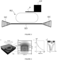
- a sensor of this type comprises an optical resonator RO, also called a photonic cavity, and one or more waveguides GO coupled to the optical resonator, as illustrated in figure 1 .
- the optical resonator is characterized by at least one resonance wavelength ⁇ r associated with a resonance bandwidth of width ⁇ r/Qopt (Qopt quality factor of the optical cavity) as illustrated in figure 2 which describes the energy E stored in the resonator as a function of wavelength.
- the propagation properties of EM waves in the optical resonator are affected by a measurand u (physical quantity to be measured) or a parameter u whose response depends on a measurand of interest z .
- a Fine reading light beam is injected at the input of the sensor, and the amplitude and/or phase of the light beam propagating in the waveguide(s) coupled to the optical resonator RO is disturbed by the magnitude u .
- the optical transmission or reflection function of the sensor is thus modified, directly or indirectly, by the physical quantity to be measured.
- the beam Fout emerges through the output of the sensor and is detected by a photodetector, and a measurement of the quantity u is deduced from the detected beam.
- the optical resonator RO is a ring whose effective propagation index n eff( u ) depends on u for its real and/or imaginary part.
- the propagation speed and/or the dissipation rate of the light wave in the optical resonator thus depend on u.
- the absorption of a biological or other body on the surface of the resonator modifies its effective propagation index and changes the position of the resonance wavelength ⁇ r( u ), u being the quantity absorbed. From the quantity absorbed we determine the nature of the body (measurand z).
- the identification of the absorbed body is carried out by the functionalization layer which selects the particles to be detected.
- the functionalization layer which selects the particles to be detected.
- the senor comprises an optical RO resonator coupled with a mechanical element whose displacement is measured.
- This type of sensor is called an optomechanical sensor.
- FIG. 3 illustrates such a sensor in which the mechanical element is a cantilever beam P fixed at one end to a stud CP.
- the reading beam is injected into the GO guide and recovered at the guide output by a GC coupling network (“grating coupler”).
- the displacement x of the beam (parameter u) in the evanescent field of the optical resonator disturbs the effective index (variation of the “gap” between the beam and the ring). From the displacement x we measure, for example, the acceleration of a body (measurand z).
- the optical resonator is coupled with a mechanical element resonant at a frequency frm.
- OMUS Optomechanical Ultrasound Sensor
- the resonant mechanical element is a Memb membrane on a thin layer of Si slab silicon, the vibration (resonance) of which is induced by an UltraS ultrasonic wave to be measured when the frequency of the wave is close to the mechanical resonance frequency frm of the membrane.
- the membrane acts as a band-pass filter which selects the spectral components of the incident wave in the vicinity of its resonance frequency.
- the membrane is placed over an RO ring also made of silicon (coupled to a GO optical guide and placed on a BOX substrate) at a distance called Gap (see a and b).
- the dark shade shows the intensity of the electromagnetic field in the vicinity of the optical resonator, the intensity is high in the region between the membrane and the resonator.
- the effective index of the neff resonator is modified by the value of the Gap (see c). When the membrane vibrates the displacement x of the membrane varies the gap and therefore the effective index.
- the UltraS wave thus modifies the value of the resonance wavelength of the optical resonator.
- This shift in resonance wavelength is read by a laser emitting a light beam at a wavelength ⁇ 0 located on one side of the resonance of the optical resonator (that is to say included in the resonance bandwidth of RO), which is injected into the waveguide.
- the light beam is detected at the guide exit by a PD photodetector.
- the shift results in a variation in the transmission T of the sensor (ratio of intensities) at wavelength ⁇ 0.
- the three curves of d correspond to different amplitudes of deflection of the membrane. Each curve corresponds to a position of the membrane. During the vibration of the latter, we move from one curve to another periodically.
- the resonant mechanical element is confused with the optical resonator, which then has an optical resonance and a mechanical resonance.
- sensors are called active sensors, because these sensors use the energy provided by the measurand to carry out the transduction, no external excitation is applied to the sensor: the force of the ultrasonic wave activates the membrane, the inertial force puts in motion the moving mass, etc.
- the resonant mechanical element is excited at an external excitation frequency fex included in the mechanical resonance band BPm around a mechanical resonance frequency frm.
- the optical resonator and the mechanical resonator are combined.
- This is for example a vibrating disk presenting both optical and mechanical resonance: for example a sensor operating in a liquid medium to detect biological objects (viruses, proteins, etc.) which are deposited on this disk.
- biological objects viruses, proteins, etc.
- We measure the additional mass absorbed on these disks we use a functionalization layer or not), which makes it possible to trace the concentration of the biological species. The mass makes the disk heavier, which changes its mechanical resonance frequency.
- it is an atomic force sensor in the form of a ring provided with a resonant tip, as described in the publication of Allain et al “Optomechanical resonating probe for very high frequency sensing of atomic forces” Nanoscale, 2020, 12, 2939 .
- Ultrasonic sensor networking allows each sensor to act as a filter by being sensitive only to its frequency range.
- information on the direction of the ultrasound wave can also be extracted through the phase shift of the signal between the sensors.
- reading a set of networked sensors is carried out by wavelength multiplexing/demultiplexing, by associating a wavelength with each sensor.
- the principle is illustrated Figure 5 .
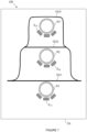
- the set of sensors is illustrated by resonators Ri whose effective index neff(ui) is modified by a measurand u (the mechanical element possibly present is not shown), coupled to the same waveguide.
- This mux/demux method is inspired by a standard signal mixing/separation procedure for telecoms (WDM for Wavelength Multiplexing Division in English).
- a multiplexer MUX mixes the beams emitted by the lasers Las1, Las2.., respectively at wavelengths ⁇ 1, ⁇ 2....
- the mixed beams are transported to the sensor network by an optical fiber OF1, and the wave F in resulting from the superposition of the different beams is injected into the GO waveguide.
- the F out wave is directed by an OF2 optical fiber to a DEMUX demultiplexer connected to photodetectors PD1, PD2... each collecting a beam at a determined wavelength.
- the document EP2866000 describes a gravimetric mass sensor consisting of a set of four vibrating plates arranged over an optical ring, forming four sensors allowing more particle masses to be measured.
- each optical resonator being associated with several mechanical elements.
- Each optical resonator/associated element pair then forms a sensor. But there is also the problem of access to the information associated with each sensor.
- An aim of the present invention is to remedy the aforementioned drawbacks by proposing a measurement system comprising several optical resonators coupled to at least one waveguide, and where appropriate several elements associated with an optical resonator, the measurement system allowing the simultaneous recovery of individual information from each elementary optical resonator/element sensor, and therefore access to all the values measured by all the sensors.
- the modulation device is arranged upstream of the injection device, the superposition of the N modulated light beams (Bmod(i)) forming the input beam.
- the transmission device comprises N lasers and the modulation device comprises N modulators arranged respectively on the optical paths of the N light beams emitted by the N lasers, each modulator being configured to modulate the light beam associated with the frequency fmod(i).
- the modulators are electro-optical modulators.
- the transmission device and the modulation device form the same device comprising N intensity-modulated lasers.
- an LIA demodulation module comprises a reference oscillator at a demodulation frequency and a first demodulation chain comprising a mixer and a low pass filter.
- an LIA demodulation module comprises a second demodulation chain in quadrature with the first chain.
- the optical resonator is chosen from: a disk, a guide looped back on itself, a photonic crystal.
- a single element is associated with each optical resonator and the demodulation device comprises N LIA demodulation modules configured to operate N demodulations at said modulation frequencies fmod(i).
- At least one element Eij is resonant and has a characteristic frequency fc(i,j) included in a resonance band of the resonant element Eij, j being the index of the element associated with the resonator Ri.
- a single element is associated with each optical resonator and the demodulation device comprises N LIA demodulation modules configured to respectively operate N demodulations at frequencies fmod(i) +/- fc(i) when fc(i) exists and at frequencies fmod(i) otherwise.
- a single element is associated with each optical resonator and the demodulation device comprises a first stage of N LIA demodulation modules (11) configured to respectively operate N demodulations at frequencies fmod(i), and a second stage comprising either spectral filters configured to operate, for each channel i for which the frequency fc(i) exists, spectral filtering around fc(i) to extract the associated characteristic signal, or LIA demodulators at frequencies fc(i).
- the element is combined with the optical resonator.
- At least one optical resonator comprises a plurality of associated elements Eij comprising resonant elements, a resonator Ri comprising Mi associated elements, the resonant assembly comprising a total of M elements.
- the demodulation device comprises M LIA demodulation modules configured to respectively operate M demodulation at frequencies fmod(i) +/- fc(i,j) when fc(i,j) exists and at frequencies fmod(i ) Otherwise.
- the demodulation device comprises a first stage comprising N LIA demodulation modules configured to respectively operate N demodulation at frequencies fmod(i) and comprises, for each channel i for which at least one characteristic frequency exists, a second stage comprising LIA demodulation modules (11) at characteristic frequencies fc(i,j).
- the demodulation device comprises a first stage comprising N LIA demodulation modules configured to respectively operate N demodulation at frequencies fmod(i) and comprises, for each channel i for which at least one characteristic frequency exists, a second stage comprising spectral filters (BPF) configured to perform spectral filtering around the characteristic frequency fc(i,j).
- N LIA demodulation modules configured to respectively operate N demodulation at frequencies fmod(i) and comprises, for each channel i for which at least one characteristic frequency exists, a second stage comprising spectral filters (BPF) configured to perform spectral filtering around the characteristic frequency fc(i,j).
- BPF spectral filters
- the characteristic frequency is a natural vibration frequency induced by the physical quantity to be measured.
- the characteristic frequency is an external excitation frequency of said element.
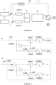
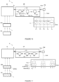
- the measurement system 10, of the MEMs and/or NEMs type, is illustrated in Figure 6 .
- the system 10 also comprises at least one element Eij coupled to each resonator Ri and configured to modify an optical transmission or reflection in the vicinity of the resonance of the associated optical resonator Ri, the modification being a function of a physical quantity to be measured.
- the optical resonators are indexed i varying from 1 to N, and the elements associated with a resonator i are indexed j: Eij.
- the number of elements associated with each resonator can be identical for all resonators (ease of manufacturing and reading) but this is not obligatory.
- a set Eij/Ri forms an elementary sensor Cij and the set ER forms a network of sensors. Within an ER assembly several types of sensors can be mixed.
- Ri resonators are: a guide looped back on itself (like a ring), a disk, a photonic crystal (periodic structuring of a dielectric element which allows light confinement).
- the optical transmission/reflection of a resonator Ri is modified by a physical quantity u, which can be either directly the final physical quantity that we wish to measure, or a parameter on which the final quantity to be measured z depends.
- the measuring system according to the invention has for objective the measurement of the physical quantity u.
- the measured value of this parameter u is called uij by the element Eij associated with the resonator Ri (sensor Cij), and it is understood that when u is an intermediate parameter, the measurement zij is then determined from uij.
- the input and the output are located at two different locations, for example at the two ends of the same waveguide.
- the input E and the output S are combined, for example in the case of a modification of the reflection.
- the resonators are arranged in series according to a waveguide, but other embodiments with more complex arrangements are possible, mixing resonators in series and/or in parallel.
- An example of a parallel arrangement is illustrated in Figure 7 (GO1, GO2 and GO3 in parallel).
- the resonant ER assembly of networked sensors is produced on a Ch chip, for example in Silicon.
- the measuring system 10 also comprises an emission device DE configured to emit a plurality of N light beams each having an emission wavelength ⁇ i included in the resonance band of the associated optical resonator Ri.
- an emission device DE configured to emit a plurality of N light beams each having an emission wavelength ⁇ i included in the resonance band of the associated optical resonator Ri.
- ⁇ i included in the resonance band of the associated optical resonator Ri.
- BPopt ⁇ r/Qopt.
- the different wavelengths ⁇ i must be chosen so as to have disjoint resonance spectral bands, to prevent a wavelength emitted by a laser from being able to address two different ROs.
- the system also includes a modulation device DM configured to modulate each of the light beams at a modulation frequency fmod(i) and an injection device DI configured to superimpose the N light beams to form an input beam Bin and to inject the input beam of the resonant assembly ER.
- the input beam Bin is the probe, or reading, beam, which will read the measurements made by the sensors Cij, via modification of the optical response of the resonators Ri.
- the beam at the output of the ER assembly is called Bout.
- the superposition of the beams is carried out for example using blades or cubes called “beam splitters” in English, or with a multiplexer called Arrayed Waveguide Grating (AWG).
- the injection into the waveguide is carried out for example with an optical fiber coupled to a diffraction grating (“grating coupler” in English) or by coupling through the edge, with an optical fiber positioned in the same plane as the substrate.
- the system also includes at least one detector Det , for example a photodiode, configured to detect a light beam coming from the output beam Bout , and generate an electrical output signal Sout.
- at least one detector Det for example a photodiode, configured to detect a light beam coming from the output beam Bout , and generate an electrical output signal Sout.
- the DM and DI devices can be integrated on the same chip, different from the chip of the ER assembly or identical.
- the Det detector can be integrated on the Ch chip of the ER assembly if necessary.
- optical beams are symbolized by a solid line and the electrical signals by a dotted line, to make the diagrams more readable.
- the modulation frequency fmod(i) of each beam is generated from a source oscillator Oscs(i).
- the modulation device is arranged upstream of the input E of ER.
- the modulated beams at the output of the device DM are called Bmod(i), and the superposition of the N modulated light beams Bmod(i) forms the input beam Bin.
- the DM device is arranged upstream of the DI device.
- the emission device DE comprises N Li lasers emitting Bini(i) beams and the modulation device DM comprises N modulators Md(i) arranged respectively on the optical paths of the N light beams emitted by the N lasers, and configured to modulate each light beams at the frequency fmod(i).
- the modulators are EOM(i) electro-optical modulators.
- the emission device DE and the modulation device DM form the same device comprising N frequency-modulated Li lasers (amplitude modulation at a given frequency), for example laser diodes powered by a modulated current.
- the DM device is then compact.
- the DM device is placed after the superposition of the beams, in the injection device.
- the modulation device is placed downstream of the output S of the assembly ER, before the detector Det.
- the modulation device performs intensity modulation.
- This intensity modulation is carried out for example directly (modulated lasers), via absorption (electro-optical modulators), via Mach Zender (MZ) type interference or resonator type interference.
- MZ Mach Zender
- This last type of modulation is compatible for positioning DM downstream of the superposition before the input E of ER, or between the output of ER and the detector.
- Intensity modulation by a March Zender MZ interferometer is a mixed method.
- the principle of the Mach Zender modulator consists of splitting in two an initial beam which travels through two branches whose phase difference ⁇ is controlled. At the output, two complementary beams in intensity are obtained using a splitter.
- the application to the measuring device according to the invention is illustrated in Figure 10 for two wavelengths ⁇ 1 and ⁇ 2 generated respectively by two lasers L1, L2.
- the phase of the optical wave of one of the branches of the interferometer is modulated, the ER assembly being placed on one of the branches, with a phase modulator MODph1 for the beam at ⁇ 1 and MODph2 for the beam at ⁇ 2.
- the ER assembly is arranged on the same branch as the phase modulators.
- the phase modulation produces an intensity modulation for each optical beam at ⁇ i.
- the signals from the complementary photodiodes PD1 and PD2 are measured.
- the advantage is to gain a factor of 2 in the output signal and to eliminate common disturbances, such as variations in laser intensity, static intensity, noise etc.
- this configuration makes it possible to minimize the optical intensity modulation in optical resonators. This intensity modulation can generate a background signal consistent with the laser modulation by localized thermal heating.
- the system 10 comprises a DDM demodulation device comprising at least N demodulation modules 11 of synchronous detection type for demodulating the output signal, so as to extract characteristic signals Sdemod(i,j) associated with each element Eij, the measured values uij of the physical quantity u being determined from the characteristic signals.
- the principle of the system according to the invention is that the information relating to a wavelength ⁇ i is coded by a frequency modulation at fmod(i), allowing the recovery of this information not by wavelength demultiplexing. but by electronic demodulation processing of the synchronous detection type. Signals at the frequencies of interest are extracted electronically with a very good signal-to-noise ratio. Extraction is carried out using analog or digital blocks.
- has in has in 1 e ⁇ j ⁇ 1 t + has in 2 e ⁇ j ⁇ 2 t + ⁇
- ⁇ i 2 ⁇ C/ ⁇ i the pulsation associated with ⁇ i (referenced in a vacuum).
- the transmission function can be linearized: With ⁇ ij complex number, u ij value of u measured by the sensor Cij and ⁇ i .
- Optical waves of different wavelengths are in fact incoherent with each other.
- the cross-intensity terms oscillate at very high frequency and have random phase differences: for these reasons they have zero mean.
- Formula (3) also shows that we can position the modulation at ⁇ i at the output of the resonant assembly, as illustrated in Figure 9 . It always involves multiplying a complex optical amplitude by a complex modulation function and by a complex transmission function of the optical resonator. The order of operations is interchangeable.
- the inventors have thus shown that thanks to the linearization of the transmission functions, the signals of interest are accessible by coding/decoding of the modulation/demodulation type according to the invention.
- the demodulated signals Sdemod(i,j) make it possible to isolate the measurands associated with each individual photonic sensor Cij because the signals are positioned on different spectral bands.
- Each wavelength “harvests” information located in the photonic chip at each optical resonator.
- the reading of information from the different sensors is simultaneous.
- the characteristic frequencies fc(i,j) must be different from each other for all j of the same optical resonator Ri.
- the principle implemented here makes it possible to position the signals associated with each optical resonator in arbitrary frequency bands which can be easily moved apart when the pulsations ⁇ i are fixed.
- the low pass bandwidth filter B P LIA integrated into the synchronous detection and placed at the output of the demodulation channel i of the LIA makes it possible to eliminate the other components distant from ⁇ j - ⁇ i >> B P LIAi .
- Synchronous detection is a well-known heterodyne signal processing technique which allows the extraction of a low amplitude and narrow band signal of known frequency in a wideband input signal Vs(t) which may be noisy.
- ADS Synchronous Detection Amplifier or “Lock In Amplifier” (LIA) in Anglo-Saxon terminology.
- the signal is amplified and multiplied by the reference (internal or external oscillator).
- a low pass filter with a suitable cutoff frequency carries out the integration.
- Synchronous detection can be carried out analog or digital.
- a coherent demodulation module or LIA 11 comprises two quadrature channels as illustrated in Figure 11 . It includes a reference oscillator Oscref, a first demodulation chain comprising a mixer Mixer1 and a low pass filter LPfilter1, and a second demodulation chain (Mixer2, LPfilter2), the two signals injected into the two mixers being phase shifted by ⁇ /2 .
- the two quadratures X and Y are digitized via ADC blocks for Analogie Digital Converter.
- the input signal is digitized by an ADC block.
- the amplitude and phase of the desired signal at frequency fref are determined from X and Y. Quadrature detection allows access to the phase and an exact calculation of the amplitude.
- the frequency fref which corresponds to the frequency of the signal extracted by the coherent demodulation module 11, is called demodulation frequency.
- LIA 11 demodulation modules The number of LIA 11 demodulation modules and the choice of different modulation and demodulation frequencies depend on the type of sensors in the ER assembly and the demodulation architecture chosen, as explained below.
- At the level of the sensor network at least one element Eij is resonant and has a characteristic frequency fc(i,j), and according to a sub-embodiment at least one optical resonator Ri comprises a plurality of elements resonant Eij (there exists at least one i for which j >1).
- the characteristic frequency is either a natural vibration frequency induced by the physical quantity to be measured, or an external excitation frequency of the element, as explained in the state of the art.
- the presence or absence of a characteristic frequency for the elements has consequences on the choice of demodulation frequencies.
- the demodulation frequency should be much higher (for example 10 times) than the bandwidth of the low pass filter of the LIA BP LIA . fdemod i > 10 . BP LIA
- the distance between two demodulation frequencies should be much greater (for example 10 times) than BP LIA : fdemod i ⁇ fdemod j > 10 .
- BP LIA fdemod i ⁇ fdemod j > 10 .
- the user can agree to reduce their measurement bandwidth to a lower level, and set the BP LIA value to a much lower value than the difference above, which ensures excellent rejection of the spurious signal in each detection channel.
- a single element Ei is associated with each optical resonator.
- the DDM demodulation device comprises N LIA demodulation modules configured to operate N demodulations at the modulation frequencies fmod(i): I out ⁇ I 1 . cos ⁇ 1 . 1 + ⁇ 1 ⁇ u 1 t + I 2 . cos ⁇ 2 . 1 + ⁇ 2 ⁇ u 2 t + I 3 . cos ⁇ 3 . 1 + ⁇ 3 ⁇ u 3 t + ...
- the demodulation frequency is synthesized from the modulation frequency, which is illustrated by the Synchro block on the Figure 12 .
- the same synthesis clock is preferably used to synchronize the different oscillators (modulation and demodulation).
- At least one element Ei is resonant at a characteristic frequency fc(i).
- the element can be confused with the optical resonator (see state of the art).
- Formula (3) is written: I out ⁇ I 1 . cos ⁇ 1 . [ 1 + ⁇ 1 ⁇ cos ⁇ 1 u 1 t + I 2 . cos ⁇ 2 . [ 1 + ⁇ 2 ⁇ cos ⁇ 2 u 2 t + I 3 . cos ⁇ 3 . [ 1 + ⁇ 3 ⁇ cos ⁇ 3 u 3 t
- the DDM demodulation device comprises N LIA demodulation modules configured to respectively operate N demodulations at frequencies fdemod(i) equal to fmod(i)+/- fc(i) when fc(i) exists, and at frequencies fmod(i) otherwise.
- fdemod(i) equal to fmod(i)+/- fc(i) when fc(i) exists, and at frequencies fmod(i) otherwise.
- a low frequency signal conditioning chain lower energy consumption, better SNR for photodiodes for example.
- demodulation frequency we will choose the demodulation frequency with the smallest absolute value.
- fmod such that fmod - fc is in the bandwidth of the packaging chain.
- conditioning chain we mean the entire processing chain between detection and determination of the desired quantity.
- the demodulation frequency is synthesized from the source oscillator generating the modulation frequency, and from an excitation oscillator generating the associated excitation frequency .
- the characteristic frequency is a natural vibration
- the natural frequency to be measured is detected (“track” in English) and used to synthesize the demodulation frequency, in combination with the modulation frequency.
- BP LIA is always less than or equal to BPc. If BP LIA is higher, it is the sensor itself which imposes the bandwidth.
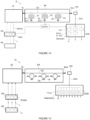
- FIG. 13 illustrates the example of a resonant assembly comprising 3 disks constituting both the optical resonator and the mechanical resonator.
- the three disks are excited respectively at the frequencies fex(1), fex(2) and fex(3), generated respectively by 3 oscillators Oscex1, Oscex2, Oscex3.
- the three excitation frequencies are respectively included in the mechanical spectral bands BPm1, BP2m, BP3m around the mechanical resonance frequencies frm1, frm2, frm3.
- the signals V1(t), V2(t) and V3(t) from the oscillators are transported on the same bus and injected into the three disks, each disk operating a filter and reacting only to its own resonance.
- the modulation frequencies fmod(1), fmod(2) and fmod(3) are generated respectively by three source oscillators Oscs1, Oscs2, Oscs3.
- the demodulation frequency fdemod(i) fmod(i)+/-fex(i) is synthesized from the two signals from the two oscillators Oscsi and Oscexi.
- the modulation frequencies are typically chosen between a few KHz and a few GHz.
- spectral filters and LIA demodulators depend on the signal you are looking for. If it is a temporal envelope, spectral filters are sufficient, if precise information on the amplitude and phase of the signal is sought, LIA demodulators must be used.
- the resonators R1 and R2 each have an element E1, E2, of respective characteristic frequency fc(1) and fc(2), and the resonator R3 has no characteristic frequency.
- Channels 1 and 2 respectively include a BPF(1) and BPF(2) filter and not channel 3. In fact for this channel 3 the signal from E3 has already been filtered by the LIA 11(3) demodulator of the first stage .
- a low pass filter can be optionally inserted after 11(3) to improve filtering.
- the modulation frequencies are typically chosen between a few tens of KHz and a few GHz.
- BP LIA BP LIA > fc + BPc
- This architecture requires higher modulation frequencies than for the previous case: it must be greater than fc and preferably 10 x fc: fmod > 10 .
- At least one optical resonator comprises a plurality of associated elements Eij including resonant elements.
- a resonator Ri comprising Mi associated elements and the resonant assembly ER comprises a total of M elements Eij.
- each element is for example beams or trays.
- each element should have a different characteristic frequency to be able to be discriminated from other elements of the same resonator.
- the demodulation device comprises M LIA demodulation modules configured to respectively operate M demodulation at frequencies fmod(i) +/- fc(i,j) when fc(i,j) exists, and at frequencies fmod(i) otherwise.
- M LIA demodulation modules configured to respectively operate M demodulation at frequencies fmod(i) +/- fc(i,j) when fc(i,j) exists, and at frequencies fmod(i) otherwise.
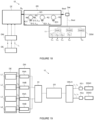
- the demodulation device in this case comprises 9 LIA demodulators 11(i,j).
- the DDM demodulation device comprises 5 LIA demodulators respectively at the demodulation frequencies: fmod+fc11, fmod+fc12, fmod+fc13, fmod+fc21, fmod.
- This single-stage architecture is preferred when one wishes to measure the amplitude and phase of the sensor signal.
- the DDM demodulation device comprises a first stage comprising N LIA demodulation modules configured to respectively operate N demodulations at frequencies fmod(i) and comprises, for each channel i for which at least one characteristic frequency exists, a second stage.
- An advantage is, for high frequency demodulation (at GHz for example), to perform only N high frequency demodulations, with a second stage dedicated to low frequency modules. We thus have a lower number of high frequency demodulations than for the single-stage case.
- the second stage includes LIA 12 demodulation modules at characteristic frequencies fc(i,j). For non-resonant elements we use a low pass filter.
- the second stage includes BPF spectral filters configured to carry out spectral filtering around the characteristic frequency fc(i,j). Likewise for non-resonant elements we use a low pass filter.
- the advantage of the 2-stage architecture is that the demodulation of the first stage is carried out at frequencies fmod(i).
- the generation of the demodulation frequency is simplified since it is equal to the modulation frequency, the two frequencies fmod(i) and fdemod(i) being synthesized from the same source oscillator.
- the demodulator 11(1) at fdemod 100 MHz makes it possible to isolate the signals from R1/E11 and R1/E12, both located at 5 and 6 MHz. A second floor allows then extract, more precisely separate, the amplitude and phase with LIA modules or the waveform with bandpass filters: the filtering width can perhaps be chosen at 10 kHz or below.
- the 11(2) demodulator does the same thing for 5 MHz and 0 Hz signals.
- the measurement system according to the invention is combined with a wavelength demultiplexing device, as illustrated in Figure 19 . This makes it possible to remove the constraint of having all different modulation frequencies.
- Lasers L1 and L3 are modulated, via a respective modulator MdA, at the same frequency fmodA, just as lasers L2 and L4 are modulated, via MdB, at the same frequency fmodB.
- the injection device superimposes all the beams and injects them into the resonant assembly ER.
- a DMUX demultiplexer component is added, which separates on the one hand the beams at ⁇ 1 and ⁇ 2 which are detected by PD1 and on the other hand the beams at ⁇ 3 and ⁇ 4 which are detected by PD2.
- Each detector PD1, PD2 is coupled to a demodulation device, respectively DDM1, DDM2. Processing of carried signals by ⁇ 1 and ⁇ 2 is carried out independently of the processing of the signals carried by ⁇ 3 and ⁇ 4.
Landscapes
- Physics & Mathematics (AREA)
- General Physics & Mathematics (AREA)
- Engineering & Computer Science (AREA)
- Microelectronics & Electronic Packaging (AREA)
- Chemical & Material Sciences (AREA)
- Optics & Photonics (AREA)
- Computer Hardware Design (AREA)
- Analytical Chemistry (AREA)
- Life Sciences & Earth Sciences (AREA)
- Geophysics (AREA)
- General Life Sciences & Earth Sciences (AREA)
- Chemical Kinetics & Catalysis (AREA)
- Plasma & Fusion (AREA)
- Health & Medical Sciences (AREA)
- Biochemistry (AREA)
- General Health & Medical Sciences (AREA)
- Immunology (AREA)
- Pathology (AREA)
- Investigating Or Analysing Materials By Optical Means (AREA)
- Gyroscopes (AREA)
- Optical Integrated Circuits (AREA)
- Micromachines (AREA)
Claims (20)
- Messsystem (10) vom Typ MEMs und/oder NEMs, das Folgendes umfasst:- eine Resonanzanordnung (ER), die Folgendes umfasst:wobei das Messsystem dadurch gekennzeichnet ist, dass es ferner Folgendes umfasst:• einen Eingang (E) und einen Ausgang (S),• eine Vielzahl von N optischen Resonatoren Ri mit Index i, die jeweils eine Resonanzwellenlänge λr,i aufweisen,• mindestens einen Wellenleiter (GO), mit dem die optischen Resonatoren gekoppelt sind,• mindestens ein Element (Ei, Eij), das mit jedem Resonator Ri gekoppelt und zum Modifizieren einer optischen Transmission oder Reflexion in der Nähe der Resonanz des optischen Resonators konfiguriert ist, wobei die Modifikation von einer zu messenden physikalischen Größe (u) abhängt,- eine Emissionsvorrichtung (DE), die zum Emittieren einer Vielzahl von N Lichtstrahlen konfiguriert ist, von denen jeder eine Emissionswellenlänge λi aufweist, die im Resonanzband des assoziierten optischen Resonators liegt,- eine Modulationsvorrichtung (DM), die zum Modulieren jedes der Lichtstrahlen mit einer Modulationsfrequenz fmod(i) konfiguriert ist,- eine Injektionsvorrichtung (DI), die zum Überlagern der N Lichtstrahlen zum Bilden eines Eingangsstrahls (Bin) und zum Injizieren des Strahls in den Eingang der Resonanzanordnung konfiguriert ist,- mindestens einen Detektor (Det), der zum Erkennen eines Lichtstrahls aus dem Ausgangsstrahl der Resonanzanordnung (Bout) und zum Erzeugen eines Ausgangssignals (Sout) konfiguriert ist,- eine Demodulationsvorrichtung (DDM), die mindestens N Demodulationsmodule (11) vom synchronen Detektionstyp, genannt LIA, zum Demodulieren des Ausgangssignals umfasst, um mit jedem Element assoziierte charakteristische Signale (Sdemod(i,j)) zu extrahieren, wobei Messwerte (uij, zij) der physikalischen Größe anhand der charakteristischen Signale bestimmt werden.
- Messsystem nach dem vorhergehenden Anspruch, wobei die Modulationsvorrichtung der Injektionsvorrichtung vorgeschaltet ist, wobei die Überlagerung der N modulierten Lichtstrahlen (Bmod(i)) den Eingangsstrahl bildet.
- Messsystem nach dem vorhergehenden Anspruch, wobei die Emissionsvorrichtung N Laser umfasst und die Modulationsvorrichtung N Modulatoren umfasst, die jeweils in den optischen Pfaden der von den N Lasern emittierten N Lichtstrahlen angeordnet sind, wobei jeder Modulator zum Modulieren des mit der Frequenz fmod(i) assoziierten Lichtstrahls konfiguriert ist.
- Messsystem nach dem vorhergehenden Anspruch, wobei die Modulatoren elektrooptische Modulatoren sind.
- Messsystem nach Anspruch 2, wobei die Emissionsvorrichtung und die Modulationsvorrichtung eine gemeinsame Vorrichtung bilden, die N intensitätsmodulierte Laser umfasst.
- Messsystem nach einem der vorhergehenden Ansprüche, wobei ein LIA-Demodulationsmodul einen Referenzoszillator mit einer Demodulationsfrequenz und eine erste Demodulationskette umfasst, die einen Mischer und ein Tiefpassfilter umfasst.
- Messsystem nach Anspruch 6, wobei ein LIA-Demodulationsmodul eine zweite Demodulationskette in Quadratur mit der ersten Kette umfasst.
- System nach einem der vorhergehenden Ansprüche, wobei der optische Resonator aus: einer Scheibe, einer in sich geschlossenen Führung, einem photonischen Kristall ausgewählt ist.
- Messsystem nach einem der vorhergehenden Ansprüche, wobei mit jedem optischen Resonator ein einzelnes Element (Ei) assoziiert ist und wobei die Demodulationsvorrichtung N LIA-Demodulationsmodule umfasst, die zum Durchführen von N Demodulationen bei den Modulationsfrequenzen fmod(i) konfiguriert sind.
- Messsystem nach einem der Ansprüche 1 bis 8, wobei mindestens ein Element Eij resonant ist und eine charakteristische Frequenz fc(i,j) aufweist, die in einem Resonanzband des Resonanzelements Eij enthalten ist, wobei j der Index des mit dem Resonator Ri assoziierten Elements ist.
- Messsystem nach Anspruch 10, wobei mit jedem optischen Resonator ein einzelnes Element (Ei) assoziiert ist und wobei die Demodulationsvorrichtung N LIA-Demodulationsmodule umfasst, konfiguriert zum jeweiligen Durchführen von N Demodulationen bei den Frequenzen fmod(i) +/- fc(i), wenn fc(i) existiert, und andernfalls bei den Frequenzen fmod(i).
- Messsystem nach Anspruch 10, wobei mit jedem optischen Resonator nur ein Element (Ei) assoziiert ist und wobei die Demodulationsvorrichtung eine erste Stufe von N LIA-Demodulationsmodulen (11), die zum jeweiligen Durchführen von N Demodulationen bei den Frequenzen fmod(i) konfiguriert sind, und eine zweite Stufe umfasst, die entweder Spektralfilter (BPF), die so konfiguriert sind, dass sie für jeden Kanal i, für den die Frequenz fc(i) existiert, eine Spektralfilterung um fc(i) zum Extrahieren des assoziierten charakteristischen Signal durchführen, oder LIA-Demodulatoren bei den Frequenzen fc(i) umfasst.
- Messsystem nach dem vorhergehenden Anspruch, wobei das Element mit dem optischen Resonator zusammenfällt.
- Messsystem nach Anspruch 10, wobei mindestens ein optischer Resonator eine Vielzahl von Resonanzelementen umfassenden assoziierten Elementen Eij umfasst, wobei ein Resonator Ri Mi assoziierte Elemente umfasst, wobei die Resonanzanordnung (ER) insgesamt M Elemente umfasst.
- System nach dem vorhergehenden Anspruch, wobei die Demodulationsvorrichtung M LIA-Demodulationsmodule umfasst, konfiguriert zum jeweiligen Durchführen von M Demodulationen bei den Frequenzen fmod(i) +/- fc(ij), wenn fc(ij) existiert, und andernfalls bei den Frequenzen fmod(i).
- Messsystem nach Anspruch 14, wobei die Demodulationsvorrichtung eine erste Stufe, die N LIA-Demodulationsmodule umfasst, die so konfiguriert sind, dass sie jeweils N Demodulationen bei den Frequenzen fmod(i) durchführen, und für jeden Kanal i, für den mindestens eine charakteristische Frequenz existiert, eine zweite Stufe umfasst, die LIA-Demodulationsmodule (11) bei den charakteristischen Frequenzen fc(i,j) umfasst.
- Messsystem nach Anspruch 14, wobei die Demodulationsvorrichtung eine erste Stufe, die N LIA-Demodulationsmodule umfasst, die so konfiguriert sind, dass sie jeweils N Demodulationen bei den Frequenzen fmod(i) durchführen, und für jeden Kanal i, für den mindestens eine charakteristische Frequenz existiert, eine zweite Stufe umfasst, die Spektralfilter (BPF) umfasst, die so konfiguriert sind, dass sie eine Spektralfilterung um die charakteristische Frequenz fc(i,j) durchführen.
- Messsystem nach einem der Ansprüche 10 bis 17, wobei die charakteristische Frequenz eine natürliche Schwingungsfrequenz ist, die durch die zu messende physikalische Größe induziert wird.
- Messsystem nach einem der Ansprüche 10 bis 17, wobei die charakteristische Frequenz eine externe Anregungsfrequenz des Elements ist.
- Verfahren zum Messen einer physikalischen Größe (u), das die folgenden Schritte umfasst:A Emittieren einer Vielzahl von N Lichtstrahlen, die jeweils eine Emissionswellenlänge λi aufweisen,B Modulieren jedes der Lichtstrahlen mit einer Modulationsfrequenz fmod(i),C Überlagern der N Lichtstrahlen zum Bilden eines Eingangsstrahls (Bin) und zum Injizieren des Strahls in den Eingang einer Resonanzanordnung,
wobei die Resonanzanordnung (ER) Folgendes umfasst:- einen Eingang (E) und einen Ausgang (S),- eine Vielzahl von N optischen Resonatoren Ri mit Index i, jeweils mit einer Resonanzwellenlänge λr,i, wobei die Wellenlänge λi innerhalb des Resonanzbandes des assoziierten optischen Resonators Ri liegt,- mindestens einen Wellenleiter (GO), mit dem die optischen Resonatoren gekoppelt sind,- mindestens ein Element (Ei, Eij), das in der Nähe jedes Resonators Ri positioniert ist,D Modifizieren einer optischen Transmission oder Reflexion in der Nähe der Resonanz jedes optischen Resonators, wobei die Modifikation von der zu messenden physikalischen Größe (u) abhängig ist,E Erkennen eines Lichtstrahls am Ausgang der Resonanzanordnung und Erzeugen eines Ausgangssignals,F synchrones Demodulieren des Ausgangssignals auf der Basis von mindestens N Demodulationsmodulen vom synchronen Detektionstyp zum Extrahieren von mit jedem Element assoziierten charakteristischen Signalen (Sdemod(ij)), wobei Messwerte (uij) der physikalischen Größe anhand der charakteristischen Signale bestimmt werden.
Applications Claiming Priority (1)
| Application Number | Priority Date | Filing Date | Title |
|---|---|---|---|
| FR2106811A FR3124592B1 (fr) | 2021-06-25 | 2021-06-25 | Système de mesure de type MEMS ou NEMS multicapteurs |
Publications (2)
| Publication Number | Publication Date |
|---|---|
| EP4109049A1 EP4109049A1 (de) | 2022-12-28 |
| EP4109049B1 true EP4109049B1 (de) | 2023-10-04 |
Family
ID=77999065
Family Applications (1)
| Application Number | Title | Priority Date | Filing Date |
|---|---|---|---|
| EP22179700.4A Active EP4109049B1 (de) | 2021-06-25 | 2022-06-17 | Messsystem vom typ mems oder nems mit mehreren sensoren |
Country Status (3)
| Country | Link |
|---|---|
| US (1) | US12448277B2 (de) |
| EP (1) | EP4109049B1 (de) |
| FR (1) | FR3124592B1 (de) |
Families Citing this family (3)
| Publication number | Priority date | Publication date | Assignee | Title |
|---|---|---|---|---|
| FR3164010A1 (fr) | 2024-06-28 | 2026-01-02 | Commissariat à l'Energie Atomique et aux Energies Alternatives | Système de mesure de type MEMs ou NEMS multicapteurs amélioré |
| FR3167451A1 (fr) * | 2024-10-16 | 2026-04-17 | Commissariat A L'energie Atomique Et Aux Energies Alternatives | Dispositif et procédé de mesure d’au moins une propriété d’un fluide |
| CN119845418B (zh) * | 2025-03-24 | 2025-06-13 | 长春理工大学 | 基于位置调控目标重建的分布式偏振探测系统与方法 |
Family Cites Families (4)
| Publication number | Priority date | Publication date | Assignee | Title |
|---|---|---|---|---|
| WO2015059511A1 (en) * | 2013-10-22 | 2015-04-30 | Commissariat à l'énergie atomique et aux énergies alternatives | Optomechanical device with mechanical elements and optical filters for actuating and/or detecting the movement of the elements |
| EP2866000B1 (de) | 2013-10-22 | 2020-03-11 | Commissariat à l'Énergie Atomique et aux Énergies Alternatives | Optomechanische Vorrichtung zum Betätigen und/oder Erkennen einer Bewegung eines mechanischen Elements, insbesondere für die gravimetrische Erfassung |
| AT518549B1 (de) * | 2016-04-06 | 2017-11-15 | Univ Wien Tech | Verfahren und Vorrichtung zur Erzeugung einer Referenzfrequenz |
| FR3050820B1 (fr) * | 2016-04-29 | 2018-04-13 | Commissariat A L'energie Atomique Et Aux Energies Alternatives | Systeme de mesure resonant a resolution amelioree |
-
2021
- 2021-06-25 FR FR2106811A patent/FR3124592B1/fr not_active Expired - Fee Related
-
2022
- 2022-06-17 EP EP22179700.4A patent/EP4109049B1/de active Active
- 2022-06-22 US US17/846,992 patent/US12448277B2/en active Active
Also Published As
| Publication number | Publication date |
|---|---|
| EP4109049A1 (de) | 2022-12-28 |
| FR3124592A1 (fr) | 2022-12-30 |
| US12448277B2 (en) | 2025-10-21 |
| FR3124592B1 (fr) | 2023-05-19 |
| US20220411257A1 (en) | 2022-12-29 |
Similar Documents
| Publication | Publication Date | Title |
|---|---|---|
| EP4109049B1 (de) | Messsystem vom typ mems oder nems mit mehreren sensoren | |
| EP3147673B1 (de) | Optomechanischer physikalischer sensor mit verbesserter empfindlichkeit | |
| EP0870180B1 (de) | Optisches bauelement zur polarisationsmodulation, und dessen verwendung in einem polarimeter oder ellipsometer | |
| FR2984491A1 (fr) | Mesure par interferometrie atomique | |
| EP3899497B1 (de) | Laservorrichtung zur polarisationsinterferometrie | |
| EP0027763B1 (de) | Verfahren und Apparat zur Abstandsmessung durch Laserinterferometrie mit zwei Wellenlängen | |
| EP3244169B1 (de) | Resonanzmesssystem mit verbesserter auflösung | |
| WO2022112679A1 (fr) | Puce photonique et composant photonique integrant une telle puce | |
| EP2569593B1 (de) | Vorrichtung zur optischen messung eines physikalischen parameters | |
| EP3201610B1 (de) | Verfahren und system zur überprüfung transparenter wafer für elektronik, optik und opto-elektronik | |
| FR3031590A1 (fr) | Capteur a fibre optique | |
| EP0601081B1 (de) | Temperaturunabhängiger Mikrosensor mit schwingendem Stab | |
| EP3071938B1 (de) | Sensor mit hochempfindlicher glasfaser | |
| EP4004597B1 (de) | Verfahren für kohärente lidar-bildgebung und zugehöriger lidar | |
| EP3462145B1 (de) | Elektromechanischer und optischer resonator | |
| EP3044697B1 (de) | Elektronisches verfahren zur extraktion der amplitude und der phase eines signals in einer synchronen detektion und interferometrische anordnung zur durchführung des verfahrens | |
| WO2013140065A1 (fr) | Système de mesure d'une zone d'écartement dans un substrat | |
| EP4671695A1 (de) | Verbessertes mems- oder nms-messsystem mit mehreren sensoren | |
| EP0522967B1 (de) | Faseroptisches Gyrometer für Navigations- und Stabilisierungszentrum | |
| FR3157734A1 (fr) | Oscillateur opto - mécanique stabilisé en température | |
| FR2817040A1 (fr) | Systeme optique et procede de mesure interferometrique a haute cadence, et circuit d'optique intergree mis en oeuvre dans le procede | |
| EP0450244A2 (de) | Detektionsvorrichtung mit optischen Fibern | |
| FR2994600A1 (fr) | Dispositif d'analyse et de reflectivite. | |
| FR2842304A1 (fr) | Interferometre a deux lasers pour mesures tachymetriques en translation |
Legal Events
| Date | Code | Title | Description |
|---|---|---|---|
| PUAI | Public reference made under article 153(3) epc to a published international application that has entered the european phase |
Free format text: ORIGINAL CODE: 0009012 |
|
| STAA | Information on the status of an ep patent application or granted ep patent |
Free format text: STATUS: REQUEST FOR EXAMINATION WAS MADE |
|
| 17P | Request for examination filed |
Effective date: 20220617 |
|
| AK | Designated contracting states |
Kind code of ref document: A1 Designated state(s): AL AT BE BG CH CY CZ DE DK EE ES FI FR GB GR HR HU IE IS IT LI LT LU LV MC MK MT NL NO PL PT RO RS SE SI SK SM TR |
|
| GRAP | Despatch of communication of intention to grant a patent |
Free format text: ORIGINAL CODE: EPIDOSNIGR1 |
|
| STAA | Information on the status of an ep patent application or granted ep patent |
Free format text: STATUS: GRANT OF PATENT IS INTENDED |
|
| RIC1 | Information provided on ipc code assigned before grant |
Ipc: G02B 6/12 20060101ALI20230503BHEP Ipc: G01N 21/77 20060101ALI20230503BHEP Ipc: G01V 8/20 20060101ALI20230503BHEP Ipc: G01V 7/00 20060101ALI20230503BHEP Ipc: G01P 15/097 20060101ALI20230503BHEP Ipc: G01P 15/093 20060101ALI20230503BHEP Ipc: G01N 21/00 20060101ALI20230503BHEP Ipc: G01L 9/00 20060101ALI20230503BHEP Ipc: G01L 1/24 20060101ALI20230503BHEP Ipc: G01L 1/10 20060101ALI20230503BHEP Ipc: G02B 6/293 20060101ALI20230503BHEP Ipc: G01D 5/26 20060101AFI20230503BHEP |
|
| INTG | Intention to grant announced |
Effective date: 20230516 |
|
| GRAS | Grant fee paid |
Free format text: ORIGINAL CODE: EPIDOSNIGR3 |
|
| GRAA | (expected) grant |
Free format text: ORIGINAL CODE: 0009210 |
|
| STAA | Information on the status of an ep patent application or granted ep patent |
Free format text: STATUS: THE PATENT HAS BEEN GRANTED |
|
| AK | Designated contracting states |
Kind code of ref document: B1 Designated state(s): AL AT BE BG CH CY CZ DE DK EE ES FI FR GB GR HR HU IE IS IT LI LT LU LV MC MK MT NL NO PL PT RO RS SE SI SK SM TR |
|
| REG | Reference to a national code |
Ref country code: GB Ref legal event code: FG4D Free format text: NOT ENGLISH |
|
| REG | Reference to a national code |
Ref country code: CH Ref legal event code: EP |
|
| REG | Reference to a national code |
Ref country code: DE Ref legal event code: R096 Ref document number: 602022000629 Country of ref document: DE |
|
| REG | Reference to a national code |
Ref country code: IE Ref legal event code: FG4D Free format text: LANGUAGE OF EP DOCUMENT: FRENCH |
|
| REG | Reference to a national code |
Ref country code: LT Ref legal event code: MG9D |
|
| REG | Reference to a national code |
Ref country code: NL Ref legal event code: MP Effective date: 20231004 |
|
| REG | Reference to a national code |
Ref country code: AT Ref legal event code: MK05 Ref document number: 1618165 Country of ref document: AT Kind code of ref document: T Effective date: 20231004 |
|
| PG25 | Lapsed in a contracting state [announced via postgrant information from national office to epo] |
Ref country code: NL Free format text: LAPSE BECAUSE OF FAILURE TO SUBMIT A TRANSLATION OF THE DESCRIPTION OR TO PAY THE FEE WITHIN THE PRESCRIBED TIME-LIMIT Effective date: 20231004 |
|
| PG25 | Lapsed in a contracting state [announced via postgrant information from national office to epo] |
Ref country code: GR Free format text: LAPSE BECAUSE OF FAILURE TO SUBMIT A TRANSLATION OF THE DESCRIPTION OR TO PAY THE FEE WITHIN THE PRESCRIBED TIME-LIMIT Effective date: 20240105 |
|
| PG25 | Lapsed in a contracting state [announced via postgrant information from national office to epo] |
Ref country code: IS Free format text: LAPSE BECAUSE OF FAILURE TO SUBMIT A TRANSLATION OF THE DESCRIPTION OR TO PAY THE FEE WITHIN THE PRESCRIBED TIME-LIMIT Effective date: 20240204 |
|
| PG25 | Lapsed in a contracting state [announced via postgrant information from national office to epo] |
Ref country code: LT Free format text: LAPSE BECAUSE OF FAILURE TO SUBMIT A TRANSLATION OF THE DESCRIPTION OR TO PAY THE FEE WITHIN THE PRESCRIBED TIME-LIMIT Effective date: 20231004 |
|
| PG25 | Lapsed in a contracting state [announced via postgrant information from national office to epo] |
Ref country code: AT Free format text: LAPSE BECAUSE OF FAILURE TO SUBMIT A TRANSLATION OF THE DESCRIPTION OR TO PAY THE FEE WITHIN THE PRESCRIBED TIME-LIMIT Effective date: 20231004 |
|
| PG25 | Lapsed in a contracting state [announced via postgrant information from national office to epo] |
Ref country code: ES Free format text: LAPSE BECAUSE OF FAILURE TO SUBMIT A TRANSLATION OF THE DESCRIPTION OR TO PAY THE FEE WITHIN THE PRESCRIBED TIME-LIMIT Effective date: 20231004 |
|
| PG25 | Lapsed in a contracting state [announced via postgrant information from national office to epo] |
Ref country code: LT Free format text: LAPSE BECAUSE OF FAILURE TO SUBMIT A TRANSLATION OF THE DESCRIPTION OR TO PAY THE FEE WITHIN THE PRESCRIBED TIME-LIMIT Effective date: 20231004 Ref country code: IS Free format text: LAPSE BECAUSE OF FAILURE TO SUBMIT A TRANSLATION OF THE DESCRIPTION OR TO PAY THE FEE WITHIN THE PRESCRIBED TIME-LIMIT Effective date: 20240204 Ref country code: GR Free format text: LAPSE BECAUSE OF FAILURE TO SUBMIT A TRANSLATION OF THE DESCRIPTION OR TO PAY THE FEE WITHIN THE PRESCRIBED TIME-LIMIT Effective date: 20240105 Ref country code: ES Free format text: LAPSE BECAUSE OF FAILURE TO SUBMIT A TRANSLATION OF THE DESCRIPTION OR TO PAY THE FEE WITHIN THE PRESCRIBED TIME-LIMIT Effective date: 20231004 Ref country code: BG Free format text: LAPSE BECAUSE OF FAILURE TO SUBMIT A TRANSLATION OF THE DESCRIPTION OR TO PAY THE FEE WITHIN THE PRESCRIBED TIME-LIMIT Effective date: 20240104 Ref country code: AT Free format text: LAPSE BECAUSE OF FAILURE TO SUBMIT A TRANSLATION OF THE DESCRIPTION OR TO PAY THE FEE WITHIN THE PRESCRIBED TIME-LIMIT Effective date: 20231004 Ref country code: PT Free format text: LAPSE BECAUSE OF FAILURE TO SUBMIT A TRANSLATION OF THE DESCRIPTION OR TO PAY THE FEE WITHIN THE PRESCRIBED TIME-LIMIT Effective date: 20240205 |
|
| PG25 | Lapsed in a contracting state [announced via postgrant information from national office to epo] |
Ref country code: SE Free format text: LAPSE BECAUSE OF FAILURE TO SUBMIT A TRANSLATION OF THE DESCRIPTION OR TO PAY THE FEE WITHIN THE PRESCRIBED TIME-LIMIT Effective date: 20231004 Ref country code: RS Free format text: LAPSE BECAUSE OF FAILURE TO SUBMIT A TRANSLATION OF THE DESCRIPTION OR TO PAY THE FEE WITHIN THE PRESCRIBED TIME-LIMIT Effective date: 20231004 Ref country code: PL Free format text: LAPSE BECAUSE OF FAILURE TO SUBMIT A TRANSLATION OF THE DESCRIPTION OR TO PAY THE FEE WITHIN THE PRESCRIBED TIME-LIMIT Effective date: 20231004 Ref country code: NO Free format text: LAPSE BECAUSE OF FAILURE TO SUBMIT A TRANSLATION OF THE DESCRIPTION OR TO PAY THE FEE WITHIN THE PRESCRIBED TIME-LIMIT Effective date: 20240104 Ref country code: LV Free format text: LAPSE BECAUSE OF FAILURE TO SUBMIT A TRANSLATION OF THE DESCRIPTION OR TO PAY THE FEE WITHIN THE PRESCRIBED TIME-LIMIT Effective date: 20231004 Ref country code: HR Free format text: LAPSE BECAUSE OF FAILURE TO SUBMIT A TRANSLATION OF THE DESCRIPTION OR TO PAY THE FEE WITHIN THE PRESCRIBED TIME-LIMIT Effective date: 20231004 |
|
| REG | Reference to a national code |
Ref country code: DE Ref legal event code: R097 Ref document number: 602022000629 Country of ref document: DE |
|
| PG25 | Lapsed in a contracting state [announced via postgrant information from national office to epo] |
Ref country code: DK Free format text: LAPSE BECAUSE OF FAILURE TO SUBMIT A TRANSLATION OF THE DESCRIPTION OR TO PAY THE FEE WITHIN THE PRESCRIBED TIME-LIMIT Effective date: 20231004 |
|
| PG25 | Lapsed in a contracting state [announced via postgrant information from national office to epo] |
Ref country code: CZ Free format text: LAPSE BECAUSE OF FAILURE TO SUBMIT A TRANSLATION OF THE DESCRIPTION OR TO PAY THE FEE WITHIN THE PRESCRIBED TIME-LIMIT Effective date: 20231004 |
|
| PG25 | Lapsed in a contracting state [announced via postgrant information from national office to epo] |
Ref country code: SK Free format text: LAPSE BECAUSE OF FAILURE TO SUBMIT A TRANSLATION OF THE DESCRIPTION OR TO PAY THE FEE WITHIN THE PRESCRIBED TIME-LIMIT Effective date: 20231004 |
|
| PG25 | Lapsed in a contracting state [announced via postgrant information from national office to epo] |
Ref country code: SM Free format text: LAPSE BECAUSE OF FAILURE TO SUBMIT A TRANSLATION OF THE DESCRIPTION OR TO PAY THE FEE WITHIN THE PRESCRIBED TIME-LIMIT Effective date: 20231004 Ref country code: SK Free format text: LAPSE BECAUSE OF FAILURE TO SUBMIT A TRANSLATION OF THE DESCRIPTION OR TO PAY THE FEE WITHIN THE PRESCRIBED TIME-LIMIT Effective date: 20231004 Ref country code: RO Free format text: LAPSE BECAUSE OF FAILURE TO SUBMIT A TRANSLATION OF THE DESCRIPTION OR TO PAY THE FEE WITHIN THE PRESCRIBED TIME-LIMIT Effective date: 20231004 Ref country code: IT Free format text: LAPSE BECAUSE OF FAILURE TO SUBMIT A TRANSLATION OF THE DESCRIPTION OR TO PAY THE FEE WITHIN THE PRESCRIBED TIME-LIMIT Effective date: 20231004 Ref country code: EE Free format text: LAPSE BECAUSE OF FAILURE TO SUBMIT A TRANSLATION OF THE DESCRIPTION OR TO PAY THE FEE WITHIN THE PRESCRIBED TIME-LIMIT Effective date: 20231004 Ref country code: DK Free format text: LAPSE BECAUSE OF FAILURE TO SUBMIT A TRANSLATION OF THE DESCRIPTION OR TO PAY THE FEE WITHIN THE PRESCRIBED TIME-LIMIT Effective date: 20231004 Ref country code: CZ Free format text: LAPSE BECAUSE OF FAILURE TO SUBMIT A TRANSLATION OF THE DESCRIPTION OR TO PAY THE FEE WITHIN THE PRESCRIBED TIME-LIMIT Effective date: 20231004 |
|
| PLBE | No opposition filed within time limit |
Free format text: ORIGINAL CODE: 0009261 |
|
| STAA | Information on the status of an ep patent application or granted ep patent |
Free format text: STATUS: NO OPPOSITION FILED WITHIN TIME LIMIT |
|
| 26N | No opposition filed |
Effective date: 20240705 |
|
| PG25 | Lapsed in a contracting state [announced via postgrant information from national office to epo] |
Ref country code: SI Free format text: LAPSE BECAUSE OF FAILURE TO SUBMIT A TRANSLATION OF THE DESCRIPTION OR TO PAY THE FEE WITHIN THE PRESCRIBED TIME-LIMIT Effective date: 20231004 |
|
| PG25 | Lapsed in a contracting state [announced via postgrant information from national office to epo] |
Ref country code: SI Free format text: LAPSE BECAUSE OF FAILURE TO SUBMIT A TRANSLATION OF THE DESCRIPTION OR TO PAY THE FEE WITHIN THE PRESCRIBED TIME-LIMIT Effective date: 20231004 |
|
| PG25 | Lapsed in a contracting state [announced via postgrant information from national office to epo] |
Ref country code: MC Free format text: LAPSE BECAUSE OF FAILURE TO SUBMIT A TRANSLATION OF THE DESCRIPTION OR TO PAY THE FEE WITHIN THE PRESCRIBED TIME-LIMIT Effective date: 20231004 |
|
| PG25 | Lapsed in a contracting state [announced via postgrant information from national office to epo] |
Ref country code: LU Free format text: LAPSE BECAUSE OF NON-PAYMENT OF DUE FEES Effective date: 20240617 |
|
| PG25 | Lapsed in a contracting state [announced via postgrant information from national office to epo] |
Ref country code: IE Free format text: LAPSE BECAUSE OF NON-PAYMENT OF DUE FEES Effective date: 20240617 |
|
| PG25 | Lapsed in a contracting state [announced via postgrant information from national office to epo] |
Ref country code: BE Free format text: LAPSE BECAUSE OF NON-PAYMENT OF DUE FEES Effective date: 20240630 |
|
| REG | Reference to a national code |
Ref country code: BE Ref legal event code: MM Effective date: 20240630 |
|
| PGFP | Annual fee paid to national office [announced via postgrant information from national office to epo] |
Ref country code: DE Payment date: 20250618 Year of fee payment: 4 |
|
| PGFP | Annual fee paid to national office [announced via postgrant information from national office to epo] |
Ref country code: FR Payment date: 20250623 Year of fee payment: 4 |
|
| PG25 | Lapsed in a contracting state [announced via postgrant information from national office to epo] |
Ref country code: FI Free format text: LAPSE BECAUSE OF FAILURE TO SUBMIT A TRANSLATION OF THE DESCRIPTION OR TO PAY THE FEE WITHIN THE PRESCRIBED TIME-LIMIT Effective date: 20231004 |
|
| PG25 | Lapsed in a contracting state [announced via postgrant information from national office to epo] |
Ref country code: CY Free format text: LAPSE BECAUSE OF FAILURE TO SUBMIT A TRANSLATION OF THE DESCRIPTION OR TO PAY THE FEE WITHIN THE PRESCRIBED TIME-LIMIT; INVALID AB INITIO Effective date: 20220617 |
|
| REG | Reference to a national code |
Ref country code: CH Ref legal event code: H13 Free format text: ST27 STATUS EVENT CODE: U-0-0-H10-H13 (AS PROVIDED BY THE NATIONAL OFFICE) Effective date: 20260127 |
|
| PG25 | Lapsed in a contracting state [announced via postgrant information from national office to epo] |
Ref country code: HU Free format text: LAPSE BECAUSE OF FAILURE TO SUBMIT A TRANSLATION OF THE DESCRIPTION OR TO PAY THE FEE WITHIN THE PRESCRIBED TIME-LIMIT; INVALID AB INITIO Effective date: 20220617 |
|
| PG25 | Lapsed in a contracting state [announced via postgrant information from national office to epo] |
Ref country code: CH Free format text: LAPSE BECAUSE OF NON-PAYMENT OF DUE FEES Effective date: 20250630 |