EP4130832A1 - Kameramodul und montageverfahren - Google Patents
Kameramodul und montageverfahren Download PDFInfo
- Publication number
- EP4130832A1 EP4130832A1 EP20938945.1A EP20938945A EP4130832A1 EP 4130832 A1 EP4130832 A1 EP 4130832A1 EP 20938945 A EP20938945 A EP 20938945A EP 4130832 A1 EP4130832 A1 EP 4130832A1
- Authority
- EP
- European Patent Office
- Prior art keywords
- connection part
- lens
- circuit board
- plane
- connection
- Prior art date
- Legal status (The legal status is an assumption and is not a legal conclusion. Google has not performed a legal analysis and makes no representation as to the accuracy of the status listed.)
- Withdrawn
Links
Images


Classifications
-
- H—ELECTRICITY
- H04—ELECTRIC COMMUNICATION TECHNIQUE
- H04N—PICTORIAL COMMUNICATION, e.g. TELEVISION
- H04N23/00—Cameras or camera modules comprising electronic image sensors; Control thereof
- H04N23/50—Constructional details
- H04N23/54—Mounting of pick-up tubes, electronic image sensors, deviation or focusing coils
-
- G—PHYSICS
- G02—OPTICS
- G02B—OPTICAL ELEMENTS, SYSTEMS OR APPARATUS
- G02B7/00—Mountings, adjusting means, or light-tight connections, for optical elements
- G02B7/003—Alignment of optical elements
-
- G—PHYSICS
- G02—OPTICS
- G02B—OPTICAL ELEMENTS, SYSTEMS OR APPARATUS
- G02B7/00—Mountings, adjusting means, or light-tight connections, for optical elements
- G02B7/003—Alignment of optical elements
- G02B7/004—Manual alignment, e.g. micromanipulators
-
- G—PHYSICS
- G02—OPTICS
- G02B—OPTICAL ELEMENTS, SYSTEMS OR APPARATUS
- G02B7/00—Mountings, adjusting means, or light-tight connections, for optical elements
- G02B7/02—Mountings, adjusting means, or light-tight connections, for optical elements for lenses
-
- G—PHYSICS
- G02—OPTICS
- G02B—OPTICAL ELEMENTS, SYSTEMS OR APPARATUS
- G02B7/00—Mountings, adjusting means, or light-tight connections, for optical elements
- G02B7/02—Mountings, adjusting means, or light-tight connections, for optical elements for lenses
- G02B7/023—Mountings, adjusting means, or light-tight connections, for optical elements for lenses permitting adjustment
-
- G—PHYSICS
- G02—OPTICS
- G02B—OPTICAL ELEMENTS, SYSTEMS OR APPARATUS
- G02B7/00—Mountings, adjusting means, or light-tight connections, for optical elements
- G02B7/02—Mountings, adjusting means, or light-tight connections, for optical elements for lenses
- G02B7/025—Mountings, adjusting means, or light-tight connections, for optical elements for lenses using glue
-
- H—ELECTRICITY
- H04—ELECTRIC COMMUNICATION TECHNIQUE
- H04N—PICTORIAL COMMUNICATION, e.g. TELEVISION
- H04N23/00—Cameras or camera modules comprising electronic image sensors; Control thereof
- H04N23/50—Constructional details
-
- H—ELECTRICITY
- H04—ELECTRIC COMMUNICATION TECHNIQUE
- H04N—PICTORIAL COMMUNICATION, e.g. TELEVISION
- H04N23/00—Cameras or camera modules comprising electronic image sensors; Control thereof
- H04N23/50—Constructional details
- H04N23/55—Optical parts specially adapted for electronic image sensors; Mounting thereof
-
- H—ELECTRICITY
- H04—ELECTRIC COMMUNICATION TECHNIQUE
- H04N—PICTORIAL COMMUNICATION, e.g. TELEVISION
- H04N23/00—Cameras or camera modules comprising electronic image sensors; Control thereof
- H04N23/57—Mechanical or electrical details of cameras or camera modules specially adapted for being embedded in other devices
-
- H—ELECTRICITY
- H05—ELECTRIC TECHNIQUES NOT OTHERWISE PROVIDED FOR
- H05K—PRINTED CIRCUITS; CASINGS OR CONSTRUCTIONAL DETAILS OF ELECTRIC APPARATUS; MANUFACTURE OF ASSEMBLAGES OF ELECTRICAL COMPONENTS
- H05K1/00—Printed circuits
- H05K1/18—Printed circuits structurally associated with non-printed electric components
- H05K1/181—Printed circuits structurally associated with non-printed electric components associated with surface mounted components
-
- H—ELECTRICITY
- H05—ELECTRIC TECHNIQUES NOT OTHERWISE PROVIDED FOR
- H05K—PRINTED CIRCUITS; CASINGS OR CONSTRUCTIONAL DETAILS OF ELECTRIC APPARATUS; MANUFACTURE OF ASSEMBLAGES OF ELECTRICAL COMPONENTS
- H05K3/00—Apparatus or processes for manufacturing printed circuits
- H05K3/30—Assembling printed circuits with electric components, e.g. with resistors
- H05K3/32—Assembling printed circuits with electric components, e.g. with resistors electrically connecting electric components or wires to printed circuits
- H05K3/321—Assembling printed circuits with electric components, e.g. with resistors electrically connecting electric components or wires to printed circuits by conductive adhesives
-
- H—ELECTRICITY
- H05—ELECTRIC TECHNIQUES NOT OTHERWISE PROVIDED FOR
- H05K—PRINTED CIRCUITS; CASINGS OR CONSTRUCTIONAL DETAILS OF ELECTRIC APPARATUS; MANUFACTURE OF ASSEMBLAGES OF ELECTRICAL COMPONENTS
- H05K2201/00—Indexing scheme relating to printed circuits covered by H05K1/00
- H05K2201/10—Details of components or other objects attached to or integrated in a printed circuit board
- H05K2201/10007—Types of components
- H05K2201/10121—Optical component, e.g. opto-electronic component
Definitions
- the present disclosure belongs to the technical field of optics, and in particular relates to a camera module and an assembling method.
- a resolution power of a lens in the camera is required to be higher and higher.
- a resolution power margin of the lens becomes smaller and smaller, that is, a focal depth range of a camera module becomes smaller and smaller, which therefore requires the precision of assembling the camera module to be higher.
- the camera modules in the non-consumer product fields are all basically fixed-focus modules (non-autofocus).
- the AA process is generally used in the industry for camera assembling.
- AA glue is an indispensable key factor: through the AA technology, after the lens and a circuit board are calibrated to the best relative positions, it is the AA glue that connects and fixes the lens and the circuit board or a base so that the lens and the circuit board are finally always kept at the best relative positions (the imaging plane of the lens coincides with a photosensitive surface of the photoelectric imaging sensor on the circuit board).
- the AA glue has a characteristic that it shrinks after curing, and the shrinkage amount is different when the thickness of the glue is different; the larger the thickness of the glue is, the larger the shrinkage amount will be.
- the shrinkage amount of the glue will still be different; the larger the thickness of the glue is, the larger the difference in the shrinkage amount will be.
- this shrinkage amount will usually be taken into consideration, and a fixed compensation amount is preset for compensation in case of the AA process.
- a fixed compensation amount is preset for compensation in case of the AA process.
- each camera module has a different thickness of the glue, so the shrinkage amount of the glue is also different. As such, when performing the compensation in case of the AA process, the compensation is performed according to the fixed compensation amount.
- the compensation is too much, and for some camera modules, the compensation is too little, which will lead to inconsistency of the resolution powers of the camera modules, making it impossible to effectively ensure that the resolution powers of all the camera modules can reach a qualified level.
- the traditional technology of AA glue shrinkage amount compensation can no longer meet this extremely high precision requirement. Therefore, for camera modules that require high-precision assembly, solving the inconsistency of AA glue thickness is very critical.
- the reason for the inconsistency of AA glue thickness is due to the deviations of various components of the camera module, the main one of which is the deviation of optical lens (specifically presented as optical back focus deviation and optical axis inclination deviation).
- the optical lens is assembled by several glasses, and further includes structural parts (spacers, lens barrels, etc.). There are tolerances between all the glasses and the structural parts, which leads to an inconsistent position of an optical focal plane of the optical lens relative to an adhesive surface of the glue, thereby directly resulting in the inconsistent thickness of the glue.
- a height deviation of the photoelectric imaging sensor and a height deviation of the base directly affect the size of AA gap, thereby affecting the thickness of the AA glue.
- An object of the present disclosure is to solve the above problems and provide a camera module and an assembling method, so as to solve the problem that the resolution power cannot be guaranteed due to the inconsistent glue thickness of the same batch of camera modules.
- the present disclosure provides a camera module, which includes a lens, a connector, a circuit board, and a photoelectric imaging sensor arranged on the circuit board; in the direction of an optical axis, the connector includes a first connection part fixedly connected with the lens, and a second connection part connected with the circuit board; a correction plane is provided on a side of the first connection part that faces the second connection part, or a correction plane is provided on a side of the second connection part that is close to the circuit board; the correction plane is parallel with an imaging plane of the lens, and a connection glue layer of a predetermined thickness is provided between the correction plane and the second connection part or between the correction plane and the circuit board.
- the second connection part is assembled with the circuit board, and the correction plane is provided on the side of the first connection part that faces the second connection part.
- the first connection part and the second connection part are integrally formed, and the correction plane is provided on the side of the second connection part that is close to the circuit board.
- the first connection part is a lens flange
- the second connection part is a lens base
- the lens is assembled with the second connection part through the first connection part
- the correction plane is provided on the side of the second connection part that is close to the circuit board.
- the present disclosure also provides an assembling method for the above-described camera module, which includes the steps of:
- the assembling method includes:
- the assembling method includes:
- the method of performing material removal processing on the first connection part or the second connection part to obtain the correction plane includes slicing, turning, cutting, milling or chemical etching.
- a correction plane is provided on a side of the first connection part that faces the second connection part, or a correction plane is provided on a side of the second connection part that faces the circuit board; the correction plane is parallel with the imaging plane of the lens, and is perpendicular to the actual optical axis of the lens, so that a gap between a lower side face of the first connection part and the second connection part (the base) is consistent, or a gap between a lower side face of the second connection part and the circuit board is consistent, thereby ensuring that in the AA process, the thickness of the filled glue is consistent, and the shrinkage amount of the glue is consistent, which solves the problem of poor resolution power of the camera module caused by the inconsistent thickness of the filled glue.
- the thickness of the connection glue layer between the correction plane and the second connection part or the circuit board is set to be the same, so that the thickness of the connection glue layer in all the camera modules is the same, and that the shrinkage amounts of all the camera modules are the same, which is advantageous for improving the consistency of the product.
- connection part of the present disclosure is provided with a sufficient size margin.
- orientations or positional relationships described by the terms “longitudinal”, “transverse”, “upper”, “lower”, “front”, “rear”, “left”, “right”, “vertical”, “horizontal”, “top”, “bottom”, “inner” and “outer” are based on the orientations or positional relationships shown in the related drawings. These terms are merely used for the sake of facilitating describing the present disclosure and simplifying the description, and do not indicate or imply that the device or element involved must have a particular orientation, or must be constructed or operated in a particular orientation. Therefore, the above terms should not be construed as limiting the present disclosure.
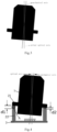
- the camera module of the present disclosure includes a lens 1, a connector 2, a circuit board 3, a photoelectric imaging sensor provided on the circuit board, and a correction plane 4.
- the connector 2 includes a first connection part 21 fixedly connected with the lens, and a second connection part 22 connected with the circuit board 3.
- the first connection part 21 and the second connection part 22 are separate members which are connected, or the first connection part 21 and the second connection part 22 are integrally formed.
- the correction plane 4 is provided on a side of the first connection part 21 that faces the second connection part 22, or on a side of the second connection part 22 that faces the circuit board 3.
- the correction plane 4 of the present disclosure is parallel with an imaging plane of the lens 1 and perpendicular to the optical axis of the lens 1.
- a connection glue layer A is provided between the correction plane 4 and the second connection part 22, or a connection glue layer A is provided between the correction plane 4 and the circuit board 3. It should be noted that for all the camera modules, the thickness of the connection glue layer A is set to be the same, that is, when assembling all the camera modules, the thickness of the filled glue used for assembling is consistent.
- the first connection part 21 and the second connection part 22 of the connector 2 are both separate members.
- the first connection part 21 is a connection flange and is fixedly connected with the lens 1
- the second connection part 22 is a lens base.
- the base is assembled with the circuit board 3, and then the lens 1 is assembled with the base and the circuit board 3 through the AA process.
- the glue (the connection glue layer) is filled to fixedly connect the first connection part 21 and the second connection part 22.
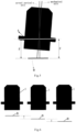
- the gap between the first connection part 21 (the connection flange) and the second connection part 22 (the base) will cause a gap between the first connection part 21 (the connection flange) and the second connection part 22 (the base) to be inconsistent in a circumferential direction.
- the gap between the first connection part 21 and a left side of the base 22 is d1
- the gap between the first connection part 21 and a right side of the base 22 is d2, where d1>d2.
- a correction plane 4 is provided on a side of the first connection part 21 that faces the second connection part 22. That is, a lower side face of the first connection part 21 is the correction plane 4, and the correction plane 4 is parallel with the imaging plane of the lens 1 and perpendicular to the actual optical axis of the lens 1, so that the gap between the lower side face of the first connection part 21 and the second connection part 22 (the base) is consistent, and that the thickness of the glue filled between the first connection part 21 and the second connection part 22 is consistent and the shrinkage amount of the glue is consistent, which solves the problem of poor resolution power of the camera module caused by the inconsistent thickness of the glue filled between the first connection part 21 and the second connection part 22.
- the thickness of the glue filled between the correction plane 4 and the second connection part 22 is set in advance, that is, the thickness of the connection glue layer A is set in advance, so that it can be ensured that the thickness of the connection glue layer in each camera module is consistent, which is advantageous for solving the problems of poor product consistency and low pass rate.
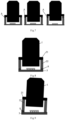
- the lens 1 in addition to the deviation that the mechanical axis does not coincide with the actual optical axis, the lens 1 also has a deviation of the imaging plane.
- a middle view of FIG. 6 indicates an ideal position of the imaging plane B of the lens 1
- a left view indicates that the imaging plane B of the lens 1 has a negative deviation
- a right view indicates that the imaging plane B of the lens 1 has a positive deviation.
- the thickness of the glue when there is a negative deviation in the back focus of the lens 1, the thickness of the glue will decrease; the larger the deviation is, the smaller the thickness will be.
- the deviation reaches a certain degree and the thickness of the glue is a negative value, it means that the lens 1 interferes with the base 22.
- the assembling of the camera cannot be carried out.
- the thickness of the glue When there is a positive deviation in the back focus of the lens 1, the thickness of the glue will increase; the larger the deviation is, the larger the thickness will be.
- the thickness of the glue is too small, the gap between the lens 1 and the base 22 will be very small, which is very likely to cause interference during the AA process and assembly failure.
- the thicknesses of the filled glues as required are different, and the shrinkage amounts of the connection glue layers of different thicknesses are different during operation, so that the quality of the camera module cannot be guaranteed.
- the larger the thickness of the glue is, the larger the shrinkage amount will be, and the larger the difference in the shrinkage amount will be.
- a focal depth range of the module is generally within a few microns. If the thickness of the glue is too large and the difference in the shrinkage amount is far larger than the focal depth range, then it cannot be ensured that the module will have good performance after the AA assembly.
- the camera module of the present disclosure can ensure that the thickness of the glue is consistent, and the thickness of the glue can be made very small, which is recommended to be below 200um. Of course, under the premise of ensuring the strength of the glue, the smaller the thickness is, the better it will be.
- the first connection part 21 and the second connection part 22 of the connector 2 are both separate members.
- the first connection part 21 is a connection flange and is fixedly connected with the lens 1
- the second connection part 22 is a base.
- the lens 1, the first connection part 21 and the second connection part 22 are assembled first, and then assembled with the circuit board 3 through the AA process. As shown in FIG.
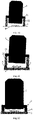
- a correction plane 4 is provided on a side of the second connection part 22 that faces the circuit board 3, that is, a lower side face of the second connection part 22 is the correction plane 4.
- the correction plane 4 is arranged parallel with an imaging plane B of the lens 1 and perpendicular to the actual optical axis of the lens 1, so that the gap between the second connection part 22 and the circuit board 3 is consistent, and that the thickness of the glue used to connect the second connection part 22 and the circuit board 3 is also consistent.
- d represents the thickness of the connection glue layer A
- F represents a distance from the correction plane 4 to the imaging plane
- h represents a height of a photosensitive surface of the photoelectric imaging sensor from an upper surface of the circuit board 3.
- the correction plane 4 is located below the imaging plane, so F is a negative value.
- the first connection part 21 and the second connection part 22 of the connector 2 are integrally formed.
- the lens 1 and the connector 2 are assembled, they are assembled with the circuit board through the AA process.
- a correction plane 4 is provided on a side of the second connection part 22 that faces the circuit board 3, that is, a lower side face of the second connection part 22 is the correction plane 4.
- the correction plane 4 is arranged parallel with an imaging plane B of the lens 1 and perpendicular to the actual optical axis of the lens 1, so that the gap between the second connection part 22 and the circuit board 3 is consistent, and that the thickness of the glue used to connect the second connection part 22 and the circuit board 3 is also consistent.
- the present disclosure also provides a method for assembling the above-described camera module, which includes the steps of: S1: assembling the lens with the connector having a size margin; S2: determining a height h of a photosensitive surface of the photoelectric imaging sensor from an upper surface of the circuit board; S3: setting the thickness d of the connection glue layer; S4: determining the imaging plane of the lens; and S5: according to the value of h obtained in the step S2 and the set value of d, and taking the imaging plane of the lens as a reference, performing material removal processing on the first connection part or the second connection part to obtain the correction plane which is a free end and which is parallel with the imaging plane, and fixing the first connection part and the second connection part through the connection glue layer or fixing the second connection part and the circuit board through the connection glue layer.
- connection part of the present disclosure is provided with sufficient size margin.
- the method of performing material removal processing on the first connection part or the second connection part to obtain the correction plane includes slicing, turning, cutting, milling or chemical etching.
Landscapes
- Engineering & Computer Science (AREA)
- Physics & Mathematics (AREA)
- Multimedia (AREA)
- Signal Processing (AREA)
- General Physics & Mathematics (AREA)
- Optics & Photonics (AREA)
- Microelectronics & Electronic Packaging (AREA)
- Manufacturing & Machinery (AREA)
- Lens Barrels (AREA)
- Studio Devices (AREA)
- Transforming Light Signals Into Electric Signals (AREA)
Applications Claiming Priority (2)
| Application Number | Priority Date | Filing Date | Title |
|---|---|---|---|
| CN202010486713.9A CN113766092B (zh) | 2020-06-01 | 2020-06-01 | 一种摄像模组及组装方法 |
| PCT/CN2020/099083 WO2021243778A1 (zh) | 2020-06-01 | 2020-06-30 | 一种摄像模组及组装方法 |
Publications (2)
| Publication Number | Publication Date |
|---|---|
| EP4130832A1 true EP4130832A1 (de) | 2023-02-08 |
| EP4130832A4 EP4130832A4 (de) | 2024-04-24 |
Family
ID=78782255
Family Applications (1)
| Application Number | Title | Priority Date | Filing Date |
|---|---|---|---|
| EP20938945.1A Withdrawn EP4130832A4 (de) | 2020-06-01 | 2020-06-30 | Kameramodul und montageverfahren |
Country Status (6)
| Country | Link |
|---|---|
| US (1) | US20230038371A1 (de) |
| EP (1) | EP4130832A4 (de) |
| JP (1) | JP7441976B2 (de) |
| KR (1) | KR20220160682A (de) |
| CN (1) | CN113766092B (de) |
| WO (1) | WO2021243778A1 (de) |
Families Citing this family (2)
| Publication number | Priority date | Publication date | Assignee | Title |
|---|---|---|---|---|
| CN116506704B (zh) * | 2023-04-12 | 2025-10-31 | 浙江大华技术股份有限公司 | 一种摄像模组及成像系统 |
| JP2025018345A (ja) * | 2023-07-26 | 2025-02-06 | パナソニックオートモーティブシステムズ株式会社 | 車載用カメラ |
Family Cites Families (17)
| Publication number | Priority date | Publication date | Assignee | Title |
|---|---|---|---|---|
| JPS61245774A (ja) * | 1985-04-24 | 1986-11-01 | Mitsubishi Electric Corp | ビデオカメラ |
| JPH11345955A (ja) * | 1998-05-29 | 1999-12-14 | Sony Corp | レンズ一体型固体撮像素子並びにそのレンズ装着方法及びレンズ装着装置 |
| JP2003163342A (ja) * | 2001-11-29 | 2003-06-06 | Olympus Optical Co Ltd | 固体撮像装置及びその製造方法 |
| JP2007184801A (ja) * | 2006-01-10 | 2007-07-19 | Alps Electric Co Ltd | カメラモジュール |
| US9638884B2 (en) * | 2014-07-02 | 2017-05-02 | Stmicroelectronics Pte Ltd | Selective component bonding technique |
| CN104270556A (zh) * | 2014-10-08 | 2015-01-07 | 信利光电股份有限公司 | 摄像模组 |
| CN105842960A (zh) * | 2015-01-13 | 2016-08-10 | 宁波舜宇光电信息有限公司 | 一种影像模组、镜座结构及其设计方法 |
| US9715078B2 (en) * | 2015-05-14 | 2017-07-25 | Microsoft Technology Licensing, Llc | Adjustable lens mount |
| CN106817515B (zh) * | 2015-11-30 | 2020-07-24 | 宁波舜宇光电信息有限公司 | 摄像模组及其结构和组装方法 |
| CN106888343A (zh) * | 2015-12-15 | 2017-06-23 | 南昌欧菲光电技术有限公司 | 摄像头模组和具有其的电子设备 |
| JP6524951B2 (ja) * | 2016-03-30 | 2019-06-05 | パナソニックIpマネジメント株式会社 | カメラモジュール |
| US10466501B2 (en) * | 2016-05-26 | 2019-11-05 | Ams Sensors Singapore Pte. Ltd. | Optoelectronic modules including an optical system tilted with respect to a focal plane |
| JP2019113711A (ja) * | 2017-12-25 | 2019-07-11 | マクセル株式会社 | レンズユニットおよびカメラモジュール |
| CN108052168A (zh) * | 2018-01-18 | 2018-05-18 | 广东欧珀移动通信有限公司 | 显示屏组件的组装方法、显示屏组件及电子设备 |
| US11220224B2 (en) * | 2018-06-13 | 2022-01-11 | Magna Electronics Inc. | Vehicular camera assembly with enhanced lens-imager joint |
| CN110830699A (zh) * | 2019-11-28 | 2020-02-21 | 宁波为森智能传感技术有限公司 | 一种摄像头 |
| CN212367351U (zh) * | 2020-06-01 | 2021-01-15 | 浙江舜宇智领技术有限公司 | 一种摄像模组 |
-
2020
- 2020-06-01 CN CN202010486713.9A patent/CN113766092B/zh active Active
- 2020-06-30 JP JP2022567536A patent/JP7441976B2/ja active Active
- 2020-06-30 WO PCT/CN2020/099083 patent/WO2021243778A1/zh not_active Ceased
- 2020-06-30 KR KR1020227038153A patent/KR20220160682A/ko not_active Ceased
- 2020-06-30 EP EP20938945.1A patent/EP4130832A4/de not_active Withdrawn
-
2022
- 2022-10-03 US US17/958,822 patent/US20230038371A1/en not_active Abandoned
Also Published As
| Publication number | Publication date |
|---|---|
| WO2021243778A1 (zh) | 2021-12-09 |
| CN113766092B (zh) | 2025-04-22 |
| EP4130832A4 (de) | 2024-04-24 |
| KR20220160682A (ko) | 2022-12-06 |
| CN113766092A (zh) | 2021-12-07 |
| JP2023524567A (ja) | 2023-06-12 |
| US20230038371A1 (en) | 2023-02-09 |
| JP7441976B2 (ja) | 2024-03-01 |
Similar Documents
| Publication | Publication Date | Title |
|---|---|---|
| US20230038371A1 (en) | Camera module and assembling method | |
| EP3684043B1 (de) | Kameramodul und zugehöriges herstellungsverfahren | |
| EP3684044B1 (de) | Kameramodul und zugehöriges herstellungsverfahren | |
| CN109116509B (zh) | 多群组镜头、摄像模组及其组装方法、电子设备 | |
| EP1246455B1 (de) | Bildaufnahmevorrichtung | |
| EP3761099A1 (de) | Optische linsenanordnung, kameramodul und montageverfahren dafür | |
| EP3828611A1 (de) | Mehrlinsenanordnung, kameramodul und verfahren zu deren herstellung | |
| US11899268B2 (en) | Optical lens, camera module and assembly method therefor | |
| CN212367351U (zh) | 一种摄像模组 | |
| CN110275263B (zh) | 光学镜头、摄像模组及其组装方法 | |
| CN101373245A (zh) | 镜片及镜头模组 | |
| CN111371971A (zh) | 一种cob摄像头模组及其封装方法 | |
| CN106550176B (zh) | 镜头调焦方法与光学模块 | |
| CN120722535B (zh) | 一种用于平面反射镜粘接同时标定角度的结构及方法 | |
| CN114721110A (zh) | 一种镜头结构 | |
| JP6992163B2 (ja) | 感光アセンブリ、イメージングモジュール、スマート端末及び感光アセンブリの製造方法と金型 | |
| CN114080554B (zh) | 用于相机模块的镜头座和凸缘设计 | |
| TW201518777A (zh) | 透鏡陣列、透鏡陣列層疊體及這些的製造方法 | |
| CN117440232A (zh) | 一种车载摄像头模组 | |
| CN114762309B (zh) | 滤光组件、摄像模组及多摄模组 | |
| CN110275264B (zh) | 光学镜头、摄像模组及其组装方法 | |
| CN119986953B (zh) | 一种应用于长焦光学系统的光转折元件及其制造工艺 | |
| CN223414928U (zh) | 一种用于提高摄像头模组平整度的结构 | |
| CN116095300A (zh) | 一种光轴对准方法及摄像模组 | |
| US7911703B2 (en) | Manufacturing method for a wafer lens module and the structure thereof |
Legal Events
| Date | Code | Title | Description |
|---|---|---|---|
| STAA | Information on the status of an ep patent application or granted ep patent |
Free format text: STATUS: THE INTERNATIONAL PUBLICATION HAS BEEN MADE |
|
| PUAI | Public reference made under article 153(3) epc to a published international application that has entered the european phase |
Free format text: ORIGINAL CODE: 0009012 |
|
| STAA | Information on the status of an ep patent application or granted ep patent |
Free format text: STATUS: REQUEST FOR EXAMINATION WAS MADE |
|
| 17P | Request for examination filed |
Effective date: 20221031 |
|
| AK | Designated contracting states |
Kind code of ref document: A1 Designated state(s): AL AT BE BG CH CY CZ DE DK EE ES FI FR GB GR HR HU IE IS IT LI LT LU LV MC MK MT NL NO PL PT RO RS SE SI SK SM TR |
|
| DAV | Request for validation of the european patent (deleted) | ||
| DAX | Request for extension of the european patent (deleted) | ||
| A4 | Supplementary search report drawn up and despatched |
Effective date: 20240326 |
|
| RIC1 | Information provided on ipc code assigned before grant |
Ipc: H05K 1/18 20060101ALI20240320BHEP Ipc: H04N 23/57 20230101ALI20240320BHEP Ipc: H04N 23/55 20230101ALI20240320BHEP Ipc: H04N 23/54 20230101ALI20240320BHEP Ipc: G02B 7/00 20210101ALI20240320BHEP Ipc: G02B 7/02 20210101AFI20240320BHEP |
|
| STAA | Information on the status of an ep patent application or granted ep patent |
Free format text: STATUS: THE APPLICATION IS DEEMED TO BE WITHDRAWN |
|
| 18D | Application deemed to be withdrawn |
Effective date: 20241015 |