EP4131146A1 - Dispositif de mise en uvre d'image de meb à super résolution et procédé associé - Google Patents
Dispositif de mise en uvre d'image de meb à super résolution et procédé associé Download PDFInfo
- Publication number
- EP4131146A1 EP4131146A1 EP22170445.5A EP22170445A EP4131146A1 EP 4131146 A1 EP4131146 A1 EP 4131146A1 EP 22170445 A EP22170445 A EP 22170445A EP 4131146 A1 EP4131146 A1 EP 4131146A1
- Authority
- EP
- European Patent Office
- Prior art keywords
- image
- cropped
- super resolution
- resolution sem
- upscaled
- Prior art date
- Legal status (The legal status is an assumption and is not a legal conclusion. Google has not performed a legal analysis and makes no representation as to the accuracy of the status listed.)
- Pending
Links
Images


Classifications
-
- G—PHYSICS
- G06—COMPUTING OR CALCULATING; COUNTING
- G06T—IMAGE DATA PROCESSING OR GENERATION, IN GENERAL
- G06T7/00—Image analysis
- G06T7/0002—Inspection of images, e.g. flaw detection
- G06T7/0004—Industrial image inspection
-
- G—PHYSICS
- G06—COMPUTING OR CALCULATING; COUNTING
- G06T—IMAGE DATA PROCESSING OR GENERATION, IN GENERAL
- G06T1/00—General purpose image data processing
- G06T1/0007—Image acquisition
-
- G—PHYSICS
- G06—COMPUTING OR CALCULATING; COUNTING
- G06T—IMAGE DATA PROCESSING OR GENERATION, IN GENERAL
- G06T11/00—Two-dimensional [2D] image generation
-
- G—PHYSICS
- G06—COMPUTING OR CALCULATING; COUNTING
- G06T—IMAGE DATA PROCESSING OR GENERATION, IN GENERAL
- G06T3/00—Geometric image transformations in the plane of the image
- G06T3/40—Scaling of whole images or parts thereof, e.g. expanding or contracting
- G06T3/4053—Scaling of whole images or parts thereof, e.g. expanding or contracting based on super-resolution, i.e. the output image resolution being higher than the sensor resolution
-
- G—PHYSICS
- G06—COMPUTING OR CALCULATING; COUNTING
- G06T—IMAGE DATA PROCESSING OR GENERATION, IN GENERAL
- G06T5/00—Image enhancement or restoration
- G06T5/20—Image enhancement or restoration using local operators
-
- G—PHYSICS
- G06—COMPUTING OR CALCULATING; COUNTING
- G06T—IMAGE DATA PROCESSING OR GENERATION, IN GENERAL
- G06T5/00—Image enhancement or restoration
- G06T5/70—Denoising; Smoothing
-
- G—PHYSICS
- G06—COMPUTING OR CALCULATING; COUNTING
- G06T—IMAGE DATA PROCESSING OR GENERATION, IN GENERAL
- G06T2207/00—Indexing scheme for image analysis or image enhancement
- G06T2207/10—Image acquisition modality
- G06T2207/10056—Microscopic image
- G06T2207/10061—Microscopic image from scanning electron microscope
-
- G—PHYSICS
- G06—COMPUTING OR CALCULATING; COUNTING
- G06T—IMAGE DATA PROCESSING OR GENERATION, IN GENERAL
- G06T2207/00—Indexing scheme for image analysis or image enhancement
- G06T2207/20—Special algorithmic details
- G06T2207/20081—Training; Learning
-
- G—PHYSICS
- G06—COMPUTING OR CALCULATING; COUNTING
- G06T—IMAGE DATA PROCESSING OR GENERATION, IN GENERAL
- G06T2207/00—Indexing scheme for image analysis or image enhancement
- G06T2207/20—Special algorithmic details
- G06T2207/20084—Artificial neural networks [ANN]
-
- G—PHYSICS
- G06—COMPUTING OR CALCULATING; COUNTING
- G06T—IMAGE DATA PROCESSING OR GENERATION, IN GENERAL
- G06T2207/00—Indexing scheme for image analysis or image enhancement
- G06T2207/30—Subject of image; Context of image processing
- G06T2207/30108—Industrial image inspection
- G06T2207/30141—Printed circuit board [PCB]
-
- G—PHYSICS
- G06—COMPUTING OR CALCULATING; COUNTING
- G06T—IMAGE DATA PROCESSING OR GENERATION, IN GENERAL
- G06T2207/00—Indexing scheme for image analysis or image enhancement
- G06T2207/30—Subject of image; Context of image processing
- G06T2207/30108—Industrial image inspection
- G06T2207/30148—Semiconductor; IC; Wafer
-
- G—PHYSICS
- G06—COMPUTING OR CALCULATING; COUNTING
- G06T—IMAGE DATA PROCESSING OR GENERATION, IN GENERAL
- G06T2207/00—Indexing scheme for image analysis or image enhancement
- G06T2207/30—Subject of image; Context of image processing
- G06T2207/30168—Image quality inspection
Definitions
- Some example embodiments relate to a super resolution scanning electron microscope (SEM) image implementing device and/or a method, e.g. a n operating method, thereof.
- SEM super resolution scanning electron microscope
- the evaluation of the process of the semiconductor device may be performed based on an image obtained through a scanning electron microscope (SEM) apparatus.
- a TAT may be decreased and the accuracy of the evaluation of the process of the semiconductor device may be increased.
- a super resolution scanning electron microscope (SEM) image implementing device that implements a super resolution SEM image with improved reliability from a low resolution SEM image.
- SEM scanning electron microscope
- some example embodiments provide a super resolution SEM image implementing method that implements a super resolution SEM image with improved reliability from a low resolution SEM image.
- some example embodiments provide a super resolution SEM image implementing system that implements a super resolution SEM image with improved reliability from a low resolution SEM image.
- a super resolution scanning electron microscope (SEM) image implementing device comprising a processor configured execute machine-readable instructions to cause the device to crop a low resolution SEM image to generate a first cropped image and a second cropped image, to upscale the first cropped image and the second cropped image to generate a first upscaled image and a second upscaled image, and to cancel noise from the first upscaled image and the second upscaled image to generate a first noise canceled image and a second noise canceled image.
- SEM super resolution scanning electron microscope
- a super resolution SEM image implementing method comprising, generating a first cropped image and a second cropped image by cropping a low resolution SEM image by processor, generating a first upscaled image and a second upscaled image by upscaling the first cropped image and the second cropped image by the processor, and generating a first noise canceled image and a second noise canceled image by canceling noise from the first upscaled image and the second upscaled image by the processor.
- a super resolution SEM image implementing system comprising, a central processing unit 200, a bus connected to the central processing unit, and a super resolution SEM image implementing device communicating with the central processing unit via the bus
- the super resolution SEM image implementing device includes, a processor configured to crop a low resolution SEM image to generate a first cropped image and a second cropped image, to upscale the first cropped image and the second cropped image to generate a first upscaled image and a second upscaled image, and to cancel noise from the first upscaled image and the second upscaled image to generate a first noise canceled image and a second noise canceled image.
- FIG. 1 is an illustrative block diagram illustrating a super resolution scanning electron microscope (SEM) image implementing system according to some example embodiments.
- SEM scanning electron microscope
- a super resolution SEM image implementing system 10 includes a central processing unit (CPU) 200 and a graphics processing unit (GPU) 300, a neural processing unit (NPU) 400, and a super resolution SEM image implementing device 100.
- CPU central processing unit
- GPU graphics processing unit
- NPU neural processing unit
- the central processing unit 200 may control an overall operation of the super resolution SEM image implementing system 10; for example, operations of other components constituting the super resolution SEM image implementing system 10.
- the super resolution SEM image implementing system 10 may include an accelerator, which is a dedicated circuit for a high-speed data operation such as an artificial intelligence (AI) data operation.
- the accelerator may include, for example, the graphics processing unit 300, the neural network processing unit 400, and/or a data processing unit (DPU) (not illustrated).
- the super resolution SEM image implementing system 10 includes the super resolution SEM image implementing device 100 that implements a low resolution SEM image as a super resolution SEM image.
- an SEM image obtained through an SEM apparatus is obtained as a super resolution image and evaluation of and/or an adjustment of a process of a semiconductor device is performed based on the super resolution image, a long turn-around time (TAT) may occur.
- TAT long turn-around time
- the evaluation of and/or an adjustment of the process of the semiconductor device is performed using a low resolution SEM image in order to decrease a TAT, accuracy of the evaluation may be decreased.
- the SEM image may be obtained during the process of semiconductor fabrication, e.g. as part of a critical-dimension (CD) measurement and/or adjustment process.
- CD critical-dimension
- the TAT may be decreased, and additionally the accuracy of the evaluation of the process of the semiconductor device may be increased.
- FIG. 2 is an illustrative block diagram illustrating a super resolution SEM image implementing device according to some example embodiments.
- the super resolution SEM image implementing device 100 includes a cropping unit 110, a buffer 112, an upscaling unit 120, a noise canceling unit 130, and a merging unit 140.
- a cropping unit 110 includes a cropping unit 110, a buffer 112, an upscaling unit 120, a noise canceling unit 130, and a merging unit 140.
- Each of the components described in FIG. 2 are illustrated as different elements; however, example embodiments are not limited thereto. Some of the functions described with reference to one or more elements in FIG. 2 may be performed by one or more other elements described in FIG. 2 .
- the functions of the elements illustrated in FIG. 2 may be performed by a processor, e.g. a processor configured to execute machine-readable instructions that, when executed, cause the processor to perform various functions.
- the cropping unit 110 may perform cropping on the low resolution SEM image. An operation of the cropping unit 110 will be described with reference to FIG. 3 .
- FIG. 3 is an illustrative view for describing a cropping operation of a cropping unit.
- the cropping unit 110 receives a first low resolution SEM image LR_S_I 1 to an N-th low resolution SEM image LR_S_I N obtained through an SEM apparatus, where N is a natural number greater than 1.
- N is a natural number greater than 1.
- an operation and an implementing method of the super resolution SEM image implementing device according to some example embodiments will be described with respect to the first low resolution SEM image LR_S_I 1, and this description may also be applied to other low resolution SEM images (e.g., the N-th low resolution SEM image LR_S_IN N).
- a low resolution SEM image may refer to an SEM image having resolution lower than/less than that of a super resolution SEM image.
- the first low resolution SEM image LR_S_I 1 received by the cropping unit 110 may be, for example, an image after an etching process for forming fins is performed with respect to a FinFET semiconductor element.
- the first low resolution SEM image LR_S_I 1 received by the cropping unit 110 may be an image after a trench etching process for forming shallow trench insulators (STIs) is performed with respect to a dynamic random access memory (DRAM) semiconductor element.
- the first low resolution SEM image LR_S_I 1 received by the cropping unit 110 may be an image after an etching process for forming gate lines is performed with respect to a NAND semiconductor element.
- the first low resolution SEM image LR_S_I 1 received by the cropping unit 110 may be an image after an etching process for forming channel holes is performed with respect to a VNAND semiconductor element.
- the first low resolution SEM image LR_S_I 1 received by the cropping unit 110 is not limited to the above-described examples, and may be an image in a processing process for various semiconductor devices.
- the cropping unit 110 may crop the first low resolution SEM image LR_S_I 1.
- the cropping unit 110 may crop the first low resolution SEM image LR_S_I 1 to generate a plurality of cropped images (first cropped image C_I 1 to sixteenth cropped image C_I 16).
- the number of cropped images generated by cropping the first low resolution SEM image LR_S_I 1 by the cropping unit 110 is not limited to 16, and may be greater than 16 or less than 16.
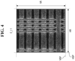
- the first cropped image C_I 1 generated by cropping the first low resolution SEM image LR_S_I 1 by the cropping unit 110 may be generated, for example, as illustrated in FIG. 4 .
- FIG. 4 is an illustrative view for describing a cropped image.
- the first cropped image C_I 1 generated by cropping the first low resolution SEM image LR_S_I 1 by the cropping unit 110 is illustrated.
- a description for the first cropped image C_I 1 may also be applied to other cropped images (second cropped image C_I 2 to sixteenth cropped image C_I 16).
- the cropping unit 110 may store a first position, which is position information on the first cropped image C_I 1, in the buffer 112.
- the buffer 112 may be implemented as a static random access memory (SRAM) buffer and/or a dynamic random access memory (DRAM) buffer; however, example embodiments are not limited thereto.
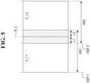
- the cropping unit 110 may store a first position including a horizontal starting point HSP, a vertical starting point VSP, a horizontal range HR, and a vertical range VR for cropping the first cropped image C_I 1, in the buffer 112.
- a horizontal starting point HSP and the vertical starting point VSP are illustrated as being in the bottom-left of the first cropped image C_I1 in FIG. 4 , example embodiments are not limited thereto, and the starting points may be at other positions in the first cropped image C_I1.
- the cropping unit 110 may crop the first low resolution SEM image LR_S_I 1 so that there are no portions overlapping each other between the plurality of cropped images (first cropped image C_I 1 to sixteenth cropped image C_I 16) generated by cropping the first low resolution SEM image LR_S_I 1.
- the plurality of cropped images may be cropped without areas overlapping each other within the first low resolution SEM image LR_S_I 1.
- the cropping unit 110 may crop the first low resolution SEM image LR_S_I 1 so that there are portions overlapping each other between the plurality of cropped images (first cropped image C_I 1 to sixteenth cropped image C_I 16) generated by cropping the first low resolution SEM image LR_S_I 1.
- FIG. 5 is an illustrative view for describing a plurality of cropped images adjacent to each other.
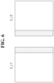
- FIG. 6 is an illustrative view for describing cropped images generated through another cropping operation of the cropping unit.
- the first cropped image C_I 1 and the second cropped image C_I 2 may be in contact with each other on the basis of/along a boundary line B_L.
- the cropping unit 110 may designate a first horizontal range HR1 from a first horizontal starting point HSP 1 where cropping starts, as a cropping area, and perform the cropping.
- the cropping unit 110 may designate a second horizontal range HR2 from a second horizontal starting point HSP 2 where cropping starts, as another cropping area, and perform the cropping.
- the cropping unit 110 may generate a first-first cropped image C_I 1' cropped so as to include an area permeating from the boundary line B_L into the second cropped image C_I 2 by a second length L2 (area patterned as diagonal lines from the upper left side to the lower right side) with respect to the first cropped image C_I 1.
- the cropping unit 110 may generate a second-first cropped image C_I 2' cropped so as to include an area permeating from the boundary line B_L into the first cropped image C_I 1 by a first length L1 (area patterned as diagonal lines from the upper right side to the lower left side) with respect to the second cropped image C_I 2.
- first length L1 and the second length L2 may be the same as, or different from each other.
- the upscaling unit 120 may upscale the plurality of cropped images (first cropped image C_I 1 to sixteenth cropped image C_I 16) generated through the cropping unit 110 to generate a plurality of upscaled images.
- FIG. 7 is an illustrative view for describing an operation of an upscaling unit.
- the upscaling unit 120 may first perform residual learning on the first cropped image C_I 1.
- the upscaling unit 120 may generate a plurality of residual blocks for stability of learning with respect to the first cropped image C_I 1.
- the upscaling unit 120 may generate 16 residual blocks.
- the upscaling unit 120 connects the front and the rear of the 16 residual blocks to each other using a skip connection for the 16 residual blocks to optimize filter parameters.
- the upscaling unit 120 may generate a first upscaled image U_I 1 through a deconvolution and/or upsampling operation. For example, an upsampling operation for an upscaling multiple of 2 may be performed. Alternatively, for example, an upsampling operation for an upscaling multiple of 4 may be performed.
- the upscaling unit 120 may generate the first upscaled image U_I 1 using a mean square error (MSE) loss function and/or a mean absolute error (MAE) loss function between the first upscaled image U_I 1 and a first ground truth image GT_I 1, generated through a deep learning-based network.
- MSE mean square error
- MAE mean absolute error
- the upscaling unit 120 may generate the first upscaled image U_I 1 using an image loss.
- the first ground truth image GT_I 1 may be a high resolution image obtained from an SEM, corresponding to the first cropped image C_I 1.
- the upscaling unit 120 may generate the first upscaled image U_I 1 using perceptual loss between the first upscaled image U_I 1 and a first ground truth image GT_I 1, generated using a convolutional neural network (CNN) such as VGGNet and/or Resnet, which are various deep learning-based image discriminator networks.
- the first ground truth image GT_I 1 may be a high resolution image obtained from an SEM, corresponding to the first cropped image C_I 1.
- a discriminator network may continuously compare the first upscaled image U_11 and the first ground truth image GT_I 1 with each other to increase resolution of the first upscaled image U_I 1.
- the first ground truth image GT_I 1 may be a high resolution image obtained from an SEM, corresponding to the first cropped image C_I 1.
- FIG. 8 is an illustrative view for describing an upscaled image generated through an upscaling operation of the upscaling unit.
- a first upscaled image U_I 1 may be generated from the first cropped image C_I 1 through the operation of the upscaling unit 120 described above.
- the noise canceling unit 130 may cancel noise from the first upscaled image U_I 1 to generate a first noise canceled image.
- FIG. 9 is an illustrative view for describing an operation of a noise canceling unit.
- the noise canceling unit 130 includes an encoder 132 performing convolution on the first upscaled image U_I 1 and a decoder 134 performing deconvolution on the first upscaled image U_I 1 on which the convolution is performed.
- a selective skip connection that connects the information of the previous layer may be applied.
- the noise canceling unit 130 may suppress loss of structural information for the first upscaled image U_I 1 received as an input of the noise canceling unit 130, and at the same time, cancel the noise from the first upscaled image U_I 1, through the selective skip connection between the encoder 132 and the decoder 134.
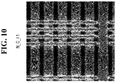
- FIG. 10 is an illustrative view for describing a noise canceled image generated through a noise canceling operation of the noise canceling unit.
- a first noise canceled image N_C_I 1 in which the noise is canceled from the first upscaled image U_I 1 may be generated through the noise canceling unit 130.
- the merging unit 140 may merge a plurality of noise canceled images (e.g., a plurality of noise canceled image including the first noise canceled image N_C_I 1) generated through the first low resolution SEM image LR_S_I 1 with each other.
- a plurality of noise canceled images e.g., a plurality of noise canceled image including the first noise canceled image N_C_I 1
- the merging unit 140 may merge the plurality of noise canceled images (e.g., the plurality of noise canceled image including the first noise canceled image N_C_I 1) with each other based on position information of each of the cropped images stored in the buffer 112.
- the plurality of noise canceled images e.g., the plurality of noise canceled image including the first noise canceled image N_C_I 1
- one first super resolution SEM image may be generated.
- FIG. 11 is an illustrative view for describing a super resolution SEM image generated through a merging unit.
- the merging unit 140 may merge the plurality of noise canceled images (e.g., the plurality of noise canceled image including the first noise canceled image N_C_I 1) generated through the first low resolution SEM image LR_S_I 1 with each other to generate a first super resolution SEM image SR_S_I.
- the plurality of noise canceled images e.g., the plurality of noise canceled image including the first noise canceled image N_C_I 1
- the merging unit 140 may merge the plurality of noise canceled images (e.g., the plurality of noise canceled image including the first noise canceled image N_C_I 1) generated through the first low resolution SEM image LR_S_I 1 with each other to generate a first super resolution SEM image SR_S_I.
- the merging unit 140 may perform merging by removing the overlapping area with respect to at least one cropped image.
- FIG. 12 is an illustrative flowchart for describing a super resolution SEM image implementing method according to some example embodiments.
- a plurality of cropped images are generated by cropping a low resolution scanning electron microscope (SEM) image through the cropping unit 110 (S100).
- SEM scanning electron microscope
- a plurality of upscaled images are generated by performing upscaling on each of the plurality of cropped images through the upscaling unit 120 (S110).
- a plurality of noise canceled images are generated by canceling noise from each of the plurality of upscaled images through the noise canceling unit 130 (S120).
- a semiconductor device may be fabricated based on the super resolution SEM image (S150).
- FIG. 13 is an illustrative graph illustrating a critical dimension (CD) distribution of the super resolution SEM image generated through the super resolution SEM image implementing method according to some example embodiments.
- CD critical dimension
- a critical dimension (CD) extracted from the super resolution (SR) SEM images generated from the low resolution SEM images through the super resolution SEM image implementing device 100 according to some example embodiments is shown on a vertical axis.
- the super resolution (SR) SEM images generated from the low resolution SEM images through the super resolution SEM image implementing device 100 are very close to the high resolution SEM images obtained from the SEM device.
- FIG. 14 is an illustrative block diagram illustrating another super resolution SEM image implementing system according to some example embodiments.
- another super resolution SEM image implementing system 12 is different from the super resolution SEM image implementing system 10 according to some example embodiments illustrated in FIG. 1 in that it further includes an anomaly detection unit 600.
- FIG. 15 is an illustrative block diagram for describing an anomaly detection unit according to some example embodiments.
- the anomaly detection unit 600 includes a training unit 610, a deep learning application unit 620, and an anomaly detector 630.
- the training unit 610 will be described with reference to FIG. 16 .
- FIG. 16 is an illustrative view for describing an operation of a training unit of the anomaly detection unit.
- the training unit 610 performs image translation learning training through comparison with a layout image based on the super resolution SEM image SR_S_I received through the super resolution SEM image implementing device 100.
- SEM image translation is performed by the deep learning application unit 620 through a deep learning model on which learning training is performed through the layout image from the training unit 610.
- FIG. 17 is an illustrative view for describing an operation of the deep learning application unit of the anomaly detection unit.
- the deep learning application unit 620 performs SEM image translation based on an image translation deep learning model on which learning training is performed from the training unit 610 using machine learning such as at least one of an artificial neural network (ANN) or using deep learning such as a deep neural network (DNN), a convolutional neural network (CNN), or a generative adversarial network.
- machine learning such as at least one of an artificial neural network (ANN) or using deep learning such as a deep neural network (DNN), a convolutional neural network (CNN), or a generative adversarial network.
- ANN artificial neural network
- DNN deep neural network
- CNN convolutional neural network
- a generative adversarial network generative adversarial network
- the anomaly detector 630 detects abnormal images through an SEM image generated by the deep learning application unit 620. An operation of the anomaly detector 630 will be described with reference to FIG. 18 .
- FIG. 18 is an illustrative block diagram for describing an operation of the anomaly detector of the anomaly detection unit.
- the anomaly detector 630 detects abnormal images through an SEM image generated by the deep learning application unit 620.
- the anomaly detector 630 may detect abnormal images in which defects are generated.
- FIG. 19 is an illustrative flowchart for describing an operation of the anomaly detection unit according to some example embodiments.
- the training unit 610 performs training through a layout image and translation learning based on the super resolution SEM image SR_S_I received through the super resolution SEM image implementing device 100 (S200).
- the deep learning application unit 620 performs SEM image translation through a layout image on which learning training is performed from the training unit 610 and a model on which learning training is performed based on an SEM image (S210).
- the anomaly detector 630 detects abnormal images through an SEM image generated by the deep learning application unit 620 (S220).
- a turn-around time (TAT) of imaging may be low.
- TAT turn-around time
- processing circuitry such as hardware including logic circuits; a hardware/software combination such as a processor executing software; or a combination thereof.
- the processing circuitry more specifically may include, but is not limited to, a central processing unit (CPU), an arithmetic logic unit (ALU), a digital signal processor, a microcomputer, a field programmable gate array (FPGA), a System-on-Chip (SoC), a programmable logic unit, a microprocessor, application-specific integrated circuit (ASIC), etc.
- the processing circuitry may include electrical components such as at least one of transistors, resistors, capacitors, etc.
- the processing circuitry may include electrical components such as logic gates including at least one of AND gates, OR gates, NAND gates, NOT gates, etc.
Landscapes
- Engineering & Computer Science (AREA)
- Physics & Mathematics (AREA)
- General Physics & Mathematics (AREA)
- Theoretical Computer Science (AREA)
- Quality & Reliability (AREA)
- Computer Vision & Pattern Recognition (AREA)
- Image Processing (AREA)
Applications Claiming Priority (2)
| Application Number | Priority Date | Filing Date | Title |
|---|---|---|---|
| KR20210102440 | 2021-08-04 | ||
| KR1020210131782A KR20230020879A (ko) | 2021-08-04 | 2021-10-05 | 고 해상도 sem 이미지 구현 장치 및 방법 |
Publications (1)
| Publication Number | Publication Date |
|---|---|
| EP4131146A1 true EP4131146A1 (fr) | 2023-02-08 |
Family
ID=81850211
Family Applications (1)
| Application Number | Title | Priority Date | Filing Date |
|---|---|---|---|
| EP22170445.5A Pending EP4131146A1 (fr) | 2021-08-04 | 2022-04-28 | Dispositif de mise en uvre d'image de meb à super résolution et procédé associé |
Country Status (4)
| Country | Link |
|---|---|
| US (1) | US12229936B2 (fr) |
| EP (1) | EP4131146A1 (fr) |
| CN (1) | CN115936981A (fr) |
| TW (1) | TW202307992A (fr) |
Citations (3)
| Publication number | Priority date | Publication date | Assignee | Title |
|---|---|---|---|---|
| US10395356B2 (en) * | 2016-05-25 | 2019-08-27 | Kla-Tencor Corp. | Generating simulated images from input images for semiconductor applications |
| US20190333199A1 (en) * | 2018-04-26 | 2019-10-31 | The Regents Of The University Of California | Systems and methods for deep learning microscopy |
| EP3686841A1 (fr) * | 2018-05-31 | 2020-07-29 | Samsung Sds Co., Ltd., | Procédé et dispositif de segmentation d'image |
Family Cites Families (8)
| Publication number | Priority date | Publication date | Assignee | Title |
|---|---|---|---|---|
| US20060291042A1 (en) | 2005-05-17 | 2006-12-28 | Alfano Robert R | Optical scanning zoom microscope with high magnification and a large field of view |
| JP5118872B2 (ja) | 2007-03-30 | 2013-01-16 | 株式会社日立ハイテクノロジーズ | 半導体デバイスの欠陥観察方法及びその装置 |
| US10648924B2 (en) | 2016-01-04 | 2020-05-12 | Kla-Tencor Corp. | Generating high resolution images from low resolution images for semiconductor applications |
| US10467729B1 (en) | 2017-10-12 | 2019-11-05 | Amazon Technologies, Inc. | Neural network-based image processing |
| KR20200030806A (ko) | 2018-09-13 | 2020-03-23 | 삼성전자주식회사 | 반도체 제조 공정을 모니터링하기 위해 인공 신경망에 기초하는 이미지 변환 모델을 포함하는 비일시적 컴퓨터 판독가능 매체 그리고 반도체 웨이퍼의 이미지를 변환하는 방법 |
| US10825650B2 (en) * | 2018-09-28 | 2020-11-03 | Taiwan Semiconductor Manufacturing Co., Ltd. | Machine learning on wafer defect review |
| KR102253227B1 (ko) | 2019-12-02 | 2021-05-18 | 포항공과대학교 산학협력단 | 저차원 재료의 원자 이미지 분석 방법 |
| US12198325B2 (en) * | 2020-04-29 | 2025-01-14 | University Of Southern California | ML-enabled assured microelectronics manufacturing: a technique to mitigate hardware trojan detection |
-
2022
- 2022-04-15 US US17/721,616 patent/US12229936B2/en active Active
- 2022-04-28 EP EP22170445.5A patent/EP4131146A1/fr active Pending
- 2022-08-02 CN CN202210921491.8A patent/CN115936981A/zh active Pending
- 2022-08-02 TW TW111128932A patent/TW202307992A/zh unknown
Patent Citations (3)
| Publication number | Priority date | Publication date | Assignee | Title |
|---|---|---|---|---|
| US10395356B2 (en) * | 2016-05-25 | 2019-08-27 | Kla-Tencor Corp. | Generating simulated images from input images for semiconductor applications |
| US20190333199A1 (en) * | 2018-04-26 | 2019-10-31 | The Regents Of The University Of California | Systems and methods for deep learning microscopy |
| EP3686841A1 (fr) * | 2018-05-31 | 2020-07-29 | Samsung Sds Co., Ltd., | Procédé et dispositif de segmentation d'image |
Non-Patent Citations (2)
| Title |
|---|
| ILESANMI ADEMOLA E. ET AL: "Methods for image denoising using convolutional neural network: a review", 10 June 2021 (2021-06-10), XP055845282, ISSN: 2199-4536, Retrieved from the Internet <URL:https://link.springer.com/content/pdf/10.1007/s40747-021-00428-4.pdf> DOI: 10.1007/s40747-021-00428-4 * |
| ZHANG HAO ET AL: "High-throughput, high-resolution deep learning microscopy based on registration-free generative adversarial network", vol. 10, no. 3, 4 February 2019 (2019-02-04), United States, pages 1044, XP055930245, ISSN: 2156-7085, Retrieved from the Internet <URL:https://opg.optica.org/DirectPDFAccess/29164761-1E2E-45AA-924C36321DC029DA_404672/boe-10-3-1044.pdf?da=1&id=404672&seq=0&mobile=no> DOI: 10.1364/BOE.10.001044 * |
Also Published As
| Publication number | Publication date |
|---|---|
| US12229936B2 (en) | 2025-02-18 |
| TW202307992A (zh) | 2023-02-16 |
| CN115936981A (zh) | 2023-04-07 |
| US20230043089A1 (en) | 2023-02-09 |
Similar Documents
| Publication | Publication Date | Title |
|---|---|---|
| CN113221895B (zh) | 小目标检测方法、装置、设备及介质 | |
| JP3028945B2 (ja) | 多階調丸め補正処理方法およびパターン検査装置 | |
| US6303251B1 (en) | Mask pattern correction process, photomask and semiconductor integrated circuit device | |
| US9430607B2 (en) | Electron beam drawing apparatus, electron beam drawing method, and storage medium | |
| KR102666072B1 (ko) | 기계 학습 장치 및 기계 학습 장치의 학습 방법 | |
| US9336587B2 (en) | Semiconductor circuit pattern measuring apparatus and method | |
| JPH08306608A (ja) | 荷電ビーム描画データ作成方法およびその作成装置 | |
| JP2015176281A (ja) | 画像処理装置および領域分割方法 | |
| EP4131146A1 (fr) | Dispositif de mise en uvre d'image de meb à super résolution et procédé associé | |
| JP2003216959A (ja) | 輪郭抽出方法及びその装置及びそのプログラム | |
| US9996906B2 (en) | Artefact detection and correction | |
| CN115829998A (zh) | 掩模图案的处理方法、装置、设备和存储介质 | |
| JPH10154648A (ja) | 荷電ビーム描画データ作成装置 | |
| CN111612690A (zh) | 一种图像拼接方法及系统 | |
| JP7758189B2 (ja) | 画像処理装置、画像処理方法、及び画像処理プログラム | |
| KR20230020879A (ko) | 고 해상도 sem 이미지 구현 장치 및 방법 | |
| JP2021051530A (ja) | 画像処理プログラム及び画像処理装置 | |
| JP2725927B2 (ja) | 荷電ビーム描画データ作成方法 | |
| JPH08221512A (ja) | 画像処理装置及びその方法 | |
| JPH08330203A (ja) | 荷電ビーム描画データ作成装置及び荷電ビーム描画システム | |
| JP2004252023A (ja) | マスクパタン生成方法およびマスクパタン生成装置 | |
| CN116416195B (zh) | 图像处理方法、计算机设备和计算机可读存储介质 | |
| US12597119B2 (en) | Operating method of electronic device including processor executing semiconductor layout simulation module based on machine learning | |
| CN111626935B (zh) | 像素图缩放方法、游戏内容生成方法及装置 | |
| CN120563567B (zh) | 一种跟踪情况下抗遮挡的处理方法及系统 |
Legal Events
| Date | Code | Title | Description |
|---|---|---|---|
| STAA | Information on the status of an ep patent application or granted ep patent |
Free format text: STATUS: EXAMINATION IS IN PROGRESS |
|
| PUAI | Public reference made under article 153(3) epc to a published international application that has entered the european phase |
Free format text: ORIGINAL CODE: 0009012 |
|
| 17P | Request for examination filed |
Effective date: 20220428 |
|
| AK | Designated contracting states |
Kind code of ref document: A1 Designated state(s): AL AT BE BG CH CY CZ DE DK EE ES FI FR GB GR HR HU IE IS IT LI LT LU LV MC MK MT NL NO PL PT RO RS SE SI SK SM TR |
|
| P01 | Opt-out of the competence of the unified patent court (upc) registered |
Effective date: 20230519 |