EP4131245A1 - Anzeigetafel und anzeigevorrichtung - Google Patents
Anzeigetafel und anzeigevorrichtung Download PDFInfo
- Publication number
- EP4131245A1 EP4131245A1 EP20897634.0A EP20897634A EP4131245A1 EP 4131245 A1 EP4131245 A1 EP 4131245A1 EP 20897634 A EP20897634 A EP 20897634A EP 4131245 A1 EP4131245 A1 EP 4131245A1
- Authority
- EP
- European Patent Office
- Prior art keywords
- bonding pads
- numbered row
- base substrate
- odd
- electrode
- Prior art date
- Legal status (The legal status is an assumption and is not a legal conclusion. Google has not performed a legal analysis and makes no representation as to the accuracy of the status listed.)
- Pending
Links
Images


Classifications
-
- H—ELECTRICITY
- H10—SEMICONDUCTOR DEVICES; ELECTRIC SOLID-STATE DEVICES NOT OTHERWISE PROVIDED FOR
- H10K—ORGANIC ELECTRIC SOLID-STATE DEVICES
- H10K59/00—Integrated devices, or assemblies of multiple devices, comprising at least one organic light-emitting element covered by group H10K50/00
- H10K59/10—OLED displays
- H10K59/12—Active-matrix OLED [AMOLED] displays
- H10K59/131—Interconnections, e.g. wiring lines or terminals
-
- G—PHYSICS
- G09—EDUCATION; CRYPTOGRAPHY; DISPLAY; ADVERTISING; SEALS
- G09G—ARRANGEMENTS OR CIRCUITS FOR CONTROL OF INDICATING DEVICES USING STATIC MEANS TO PRESENT VARIABLE INFORMATION
- G09G3/00—Control arrangements or circuits, of interest only in connection with visual indicators other than cathode-ray tubes
- G09G3/20—Control arrangements or circuits, of interest only in connection with visual indicators other than cathode-ray tubes for presentation of an assembly of a number of characters, e.g. a page, by composing the assembly by combination of individual elements arranged in a matrix no fixed position being assigned to or needed to be assigned to the individual characters or partial characters
- G09G3/34—Control arrangements or circuits, of interest only in connection with visual indicators other than cathode-ray tubes for presentation of an assembly of a number of characters, e.g. a page, by composing the assembly by combination of individual elements arranged in a matrix no fixed position being assigned to or needed to be assigned to the individual characters or partial characters by control of light from an independent source
- G09G3/36—Control arrangements or circuits, of interest only in connection with visual indicators other than cathode-ray tubes for presentation of an assembly of a number of characters, e.g. a page, by composing the assembly by combination of individual elements arranged in a matrix no fixed position being assigned to or needed to be assigned to the individual characters or partial characters by control of light from an independent source using liquid crystals
-
- H—ELECTRICITY
- H10—SEMICONDUCTOR DEVICES; ELECTRIC SOLID-STATE DEVICES NOT OTHERWISE PROVIDED FOR
- H10W—GENERIC PACKAGES, INTERCONNECTIONS, CONNECTORS OR OTHER CONSTRUCTIONAL DETAILS OF DEVICES COVERED BY CLASS H10
- H10W72/00—Interconnections or connectors in packages
-
- H—ELECTRICITY
- H10—SEMICONDUCTOR DEVICES; ELECTRIC SOLID-STATE DEVICES NOT OTHERWISE PROVIDED FOR
- H10K—ORGANIC ELECTRIC SOLID-STATE DEVICES
- H10K77/00—Constructional details of devices covered by this subclass and not covered by groups H10K10/80, H10K30/80, H10K50/80 or H10K59/80
- H10K77/10—Substrates, e.g. flexible substrates
-
- H—ELECTRICITY
- H10—SEMICONDUCTOR DEVICES; ELECTRIC SOLID-STATE DEVICES NOT OTHERWISE PROVIDED FOR
- H10W—GENERIC PACKAGES, INTERCONNECTIONS, CONNECTORS OR OTHER CONSTRUCTIONAL DETAILS OF DEVICES COVERED BY CLASS H10
- H10W72/00—Interconnections or connectors in packages
- H10W72/071—Connecting or disconnecting
- H10W72/075—Connecting or disconnecting of bond wires
- H10W72/07551—Connecting or disconnecting of bond wires characterised by changes in properties of the bond wires during the connecting
- H10W72/07554—Connecting or disconnecting of bond wires characterised by changes in properties of the bond wires during the connecting changes in dispositions
-
- H—ELECTRICITY
- H10—SEMICONDUCTOR DEVICES; ELECTRIC SOLID-STATE DEVICES NOT OTHERWISE PROVIDED FOR
- H10W—GENERIC PACKAGES, INTERCONNECTIONS, CONNECTORS OR OTHER CONSTRUCTIONAL DETAILS OF DEVICES COVERED BY CLASS H10
- H10W72/00—Interconnections or connectors in packages
- H10W72/50—Bond wires
- H10W72/541—Dispositions of bond wires
- H10W72/5445—Dispositions of bond wires being orthogonal to a side surface of the chip, e.g. parallel arrangements
-
- H—ELECTRICITY
- H10—SEMICONDUCTOR DEVICES; ELECTRIC SOLID-STATE DEVICES NOT OTHERWISE PROVIDED FOR
- H10W—GENERIC PACKAGES, INTERCONNECTIONS, CONNECTORS OR OTHER CONSTRUCTIONAL DETAILS OF DEVICES COVERED BY CLASS H10
- H10W72/00—Interconnections or connectors in packages
- H10W72/50—Bond wires
- H10W72/541—Dispositions of bond wires
- H10W72/547—Dispositions of multiple bond wires
-
- Y—GENERAL TAGGING OF NEW TECHNOLOGICAL DEVELOPMENTS; GENERAL TAGGING OF CROSS-SECTIONAL TECHNOLOGIES SPANNING OVER SEVERAL SECTIONS OF THE IPC; TECHNICAL SUBJECTS COVERED BY FORMER USPC CROSS-REFERENCE ART COLLECTIONS [XRACs] AND DIGESTS
- Y02—TECHNOLOGIES OR APPLICATIONS FOR MITIGATION OR ADAPTATION AGAINST CLIMATE CHANGE
- Y02E—REDUCTION OF GREENHOUSE GAS [GHG] EMISSIONS, RELATED TO ENERGY GENERATION, TRANSMISSION OR DISTRIBUTION
- Y02E10/00—Energy generation through renewable energy sources
- Y02E10/50—Photovoltaic [PV] energy
- Y02E10/549—Organic PV cells
Definitions
- the present disclosure relates to the field of display technologies, and in particular, to a display panel and a display device including the display panel.
- Embodiments of the present disclosure provide a display panel and a display device including the display panel.
- a display panel including:
- the plurality of first bonding pads and the plurality of second bonding pads are connected in a one-to-one correspondence via two ends of the plurality of connecting wires.
- At least one of the following are disposed in a staggered manner: the first bonding pads connected to two adjacent connecting wires among the plurality of connecting wires; or the second bonding pads connected to two adjacent connecting wires among the plurality of connecting wires.
- the plurality of first bonding pads includes a plurality of first odd-numbered row bonding pads and a plurality of first even-numbered row bonding pads.
- the plurality of first odd-numbered row bonding pads are closer to an edge of the display area than the plurality of first even-numbered row bonding pads; or the plurality of first even-numbered row bonding pads are closer to the edge of the display area than the plurality of first odd-numbered row bonding pads.
- the plurality of second bonding pads includes a plurality of second odd-numbered row bonding pads and a plurality of second even-numbered row bonding pads.
- the plurality of second odd-numbered row bonding pads are closer to the edge of the display area than the plurality of second even-numbered row bonding pads; or the plurality of second even-numbered row bonding pads are closer to the edge of the display area than the plurality of second odd-numbered row bonding pads.
- the first bonding pads and the second bonding pads connected to two adjacent connecting wires among the plurality of connecting wires are both disposed in a staggered manner.
- the plurality of first bonding pads includes the plurality of first odd-numbered row bonding pads and the plurality of first even-numbered row bonding pads
- the plurality of second bonding pads includes the plurality of second odd-numbered row bonding pads and the plurality of second even-numbered row bonding pads
- the plurality of first odd-numbered row bonding pads are closer to the edge of the display area than the plurality of first even-numbered row bonding pads
- the plurality of second odd-numbered row bonding pads are closer to the edge of the display area than the plurality of second even-numbered row bonding pads
- the plurality of first odd-numbered row bonding pads are farther away from the edge of the display area than the plurality of first even-numbered row bonding pads
- the plurality of second odd-numbered row bonding pads are farther away from the edge of the display area than the plurality of second even-numbered row bonding pads.
- the plurality of first bonding pads includes the plurality of first odd-numbered row bonding pads and the plurality of first even-numbered row bonding pads
- the plurality of second bonding pads includes the plurality of second odd-numbered row bonding pads and the plurality of second even-numbered row bonding pads
- the plurality of first odd-numbered row bonding pads are closer to the edge of the display area than the plurality of first even-numbered row bonding pads
- the plurality of second odd-numbered row bonding pads are farther away from the edge of the display area than the plurality of second even-numbered row bonding pads
- the plurality of first odd-numbered row bonding pads are farther away from the edge of the display area than the plurality of first even-numbered row bonding pads
- the plurality of second odd-numbered row bonding pads are closer to the edge of the display area than the plurality of second even-numbered row bonding pads.
- the plurality of first bonding pads are arranged in three or four rows in a staggered manner, and/or the plurality of second bonding pads are arranged in three or four rows in a staggered manner.
- wire lengths of the plurality of connecting wires are the same.
- the plurality of first bonding pads and the plurality of second bonding pads are respectively arranged in a row, and the wire lengths of two adjacent connecting wires are different.
- the plurality of first bonding pads have a golden finger structure.
- the base substrate is a silicon substrate.
- the light-emitting functional layer includes:
- the first electrode is an anode
- the second electrode is a cathode
- a display device including the above-mentioned display panel.
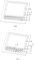
- FIG. 1 is a schematic structural diagram of an exemplary implementation of a display panel in the related art, and as shown in FIG. 1 , a base substrate 4 is disposed on a circuit board assembly 6, and a plurality of first bonding pads 1 are disposed on the circuit board assembly 6. The first bonding pads 1 are arranged in a line. A plurality of second bonding pads 3 are disposed in a non-display area 41 of the base substrate 4, and the second bonding pads 3 are arranged in a line. A plurality of connecting wires 2 are bent into arch shapes, and two ends of each connecting wire 2 are connected to a corresponding first bonding pad 1 and a corresponding second bonding pad 3 respectively.
- the connecting wire 2 may be inclined due to a lateral force of flowing filler gum, and two adjacent wires are easily overlapped together, leading to wire bonding short. As a result, yield of the silicon-based OLED display device is reduced.
- the display panel may include a base substrate 4, a circuit board assembly 6, a plurality of sub-pixels, a plurality of second bonding pads 3 and a plurality of connecting wires 2.
- the base substrate 4 includes a display area 42 and a non-display area 41 surrounding the display area 42.
- the plurality of sub-pixels are disposed in the display area 42 and located on one side of the base substrate 4. At least one of the sub-pixels includes a light-emitting element and a driving circuit.
- the light-emitting element includes a first electrode 81, a light-emitting functional layer 11 and a second electrode 82 stacked in sequence, the first electrode 81 is closer to the base substrate 4 than the second electrode 82.
- the driving circuit is located between the light-emitting element and the base substrate 4, and includes a driving transistor, a storage capacitor, and a third electrode 83.
- the driving transistor includes a source 71, a drain 72, and a gate 73. One of the source 71 and the drain 72 is coupled to the third electrode 83, the third electrode 83 is coupled to the first electrode 81, and the gate 73 is coupled to the storage capacitor.
- the circuit board assembly 6 is located on a side of the base substrate 4 facing away from the light-emitting element, and may include a plurality of first bonding pads 1.
- the plurality of second bonding pads 3 are located in the non-display area 41 of the base substrate 4.
- the first bonding pads 1 and the second bonding pads 3 are connected via the connecting wires 2, and adjacent connecting wires among the connecting wires 2 have different maximum stretchable heights in a direction perpendicular to the base substrate 4.
- the circuit board assembly 6 provides electrical signals to the sub-pixels via the connecting wires 2.
- the display panel may be the silicon-based OLED display panel, which has advantages such as small size and high resolution, and is widely applied to near-eye display devices such as a virtual reality (VR) display device and an augmented reality (AR) display device.
- the display panel may include the base substrate 4, a pixel driving circuit, the light emitting element, a first encapsulation layer module 91, a color film layer 10, a second encapsulation layer module 92, and a cover plate 5.
- the base substrate 4 includes the display area 42 and the non-display area 41 surrounding the display area 42.
- the plurality of second bonding pads 3 are disposed in the non-display area 41 of the base substrate 4.
- the plurality of sub-pixels are disposed in the display area 42. At least one of the sub-pixels includes: the source 71 and the drain 72 disposed on the base substrate 4; a first insulating layer 14 disposed on a side of the source 71 and the drain 72 facing away from the base substrate and the gate 73 disposed on a side of the first insulating layer facing away from the base substrate.
- the source 71, the drain 72 and the gate 73 form the driving transistor.
- the gate 73 is coupled to the storage capacitor (not shown in the figure).
- a second insulating layer 15 is disposed on a side of the gate 73 facing away from the base substrate 4, and a conductor layer is disposed on a side of the second insulating layer 15 facing away from the base substrate.
- the conductor layer may include the third electrode 83, a fifth electrode 85, and a sixth electrode.
- the second bonding pads 3 and the conductor layer are formed by a same patterning process.
- the third electrode 83 is coupled to the source 71 through a via connection portion 12 in the insulating layer
- the drain 72 is coupled to the fifth electrode 85 through the via connection portion 12 in the insulating layer
- the gate 73 is coupled to the sixth electrode.
- the source 71 and the drain 72 can be interchanged.
- a third insulating layer 16 is disposed on a side of the third electrode 83 facing away from the base substrate 4, and a fourth electrode 84 is disposed on a side of the third insulating layer 16 facing away from the base substrate 4.
- the fourth electrode 84 is connected to the third electrode 83 connected to the source 71 through a tungsten via connection portion 13.
- a fourth insulating layer 17 is disposed on a side of the fourth electrode 84 facing away from the base substrate 4, and the light emitting element is disposed on a side of the fourth insulating layer 17 facing away from the base substrate.
- the light-emitting element includes the first electrode 81, the light-emitting functional layer 11, and the second electrode 82 stacked in sequence, and the first electrode 81 is closer to the base substrate 4 than the second electrode 82.
- the first electrode 81 is coupled to the third electrode 83 via the fourth electrode 84.
- the first encapsulation layer module 91 is disposed on a side of the light-emitting element facing away from the base substrate 4, and the color film layer 10 is disposed on a side of the first encapsulation layer module 91 facing away from the base substrate 4.
- the second encapsulation layer module 92 is disposed on a side of the color film layer 10 facing away from the base substrate 4, and the cover plate 5 is disposed on a side of the second encapsulation layer module 92 facing away from the base substrate 4.
- Materials of the third electrode 83 and the fourth electrode 84 may include an aluminum layer and a protective layer disposed on one or both sides of the aluminum layer.
- a material of the protective layer may be TiN or Ti.
- the third electrode may function as a reflective layer.
- the gate is a poly-silicon gate grown by a molecular beam epitaxy process, and is conductive.
- the first electrode 81 is an anode.
- the material of the first electrode 81 can be a transparent conductive material such as ITO (Indium Tin Oxide), IZO (Indium Zinc Oxide), IGO (Indium Gallium Oxide).
- the material of the first electrode can also be Ti/Al/Ti/Mo or Ti/Ag/ITO.
- the second electrode 82 is a cathode, and the material of the second electrode 82 may also be a transparent conductive material such as ITO (Indium Tin Oxide), IZO (Indium Zinc Oxide), IGO (Indium Gallium Oxide), etc.
- the light-emitting functional layer 11 may include a hole injection layer, a hole transport layer, an organic light emitting layer, an electron transport layer, and an electron injection layer.
- the hole injection layer is disposed on a side of the first electrode 81 facing away from the base substrate 4, the hole transport layer is disposed on a side of the hole injection layer facing away from the base substrate 4; the organic light emitting layer is disposed on a side of the hole transport layer facing away from the base substrate 4; the electron transport layer is disposed on a side of the organic light emitting layer facing away from base substrate 4; the electron injection layer is disposed on a side of the electron transport layer facing away from the base substrate 4.
- a specific manufacturing process of the silicon-based OLED display substrate is as follows: providing the base substrate with a wafer; forming the driving circuit, the first electrode 81, the hole injection layer, the hole transport layer, the organic light emitting layer, the electron transport layer, and the electron injection layer, the second electrode 82, the first encapsulation layer module 91, the color film layer 10 and the second encapsulation layer module 92 in the sequence on the wafer; then attaching the cover plate 5 and performing cutting to form a plurality of silicon-based OLED display substrates.
- an edge of the circuit board assembly 6, an edge of the base substrate 4 and an edge of the display area 42 are all parallel to each other.
- the circuit board assembly 6 includes a printed circuit board and various components disposed on the printed circuit board.
- the circuit board assembly 6 can be formed by PCBA (Printed Circuit Board Assembly), that is, various components are assembled on the printed circuit board by the surface packaging process.
- PCBA Print Circuit Board Assembly
- the circuit board assembly 6 is formed as follows: the components are placed on an empty printed circuit board by SMT (Surface Mount Technology), and are mounted by DIP (dual inline-pin package).
- the plurality of first bonding pads 1 are disposed on the circuit board assembly 6.
- the plurality of first bonding pads 1 are disposed in a golden finger structure, and many rectangular metal contacts are arranged in rows on the printed circuit board near the edge.
- a NiAu layer is electroplated on a copper surface of the printed circuit board to form the metal contacts.
- These metal contacts are part of the printed circuit board, and the surface thereof is electroplated with the NiAu and the shape thereof is like fingers, so they are called as golden fingers.
- the golden fingers are used for connecting printed circuit boards, and can connect a circuit and transmit signals.
- two adjacent ones among the first bonding pads 1 are disposed in a staggered manner so that the first bonding pads 1 are arranged in two rows. That is, assuming that the first bonding pads 1 are marked with serial numbers "1, 2, 3, 4, 5, 6" one by one from left to right, the first bonding pads 1 with the odd numbers are called as first odd-numbered row bonding pads, and the first bonding pads 1 with the even numbers are called as first even-numbered row bonding pads.
- the first bonding pads 1 with the odd numbers are arranged in a row which is in parallel with the edge of the base substrate 4.
- the first bonding pads 1 with the even numbers are arranged in another row which is in parallel with the edge of the base substrate 4.
- a distance between the first bonding pads 1 with the odd numbers and the edge of the base substrate 4 is smaller than a distance between the first bonding pads 1 with the even numbers and the edge of the base substrate 4, that is, the first bonding pads 1 with the even numbers are moved towards a direction away from the base substrate 4 by about 1 mm to 2 mm, for example, 1.5 mm. Therefore, the first odd-numbered row bonding pads are closer to the edge of the display area 42 than the first even-numbered row bonding pads.
- An arrangement structure of the plurality of first bonding pads 1 is not limited to the above description.
- the distance between the first bonding pads 1 with the odd numbers and the edge of the base substrate 4 may be larger than the distance between the first bonding pads 1 with the even numbers and the edge of the base substrate 4, so that the first even-numbered row bonding pads are closer to the edge of the display area 42 than the first odd-numbered row bonding pads.
- the first bonding pads 1 can also be arranged in three rows, four rows or more rows.
- the first bonding pads 1 can also be disposed in a jagged form, as long as two adjacent first bonding pads 1 are disposed in the staggered manner.
- the second bonding pads 3 may be disposed in a row.
- FIG. 2 where the first bonding pads 1 are disposed in two rows in the staggered manner and the connecting wires 2 have the same length, after a first end of each connecting wire being connected to a first bonding pad 1 and a second end of each connecting wire 2 being connected to a second bonding pad 3, two adjacent connecting wires 2 are made to have different maximum stretchable heights in a direction perpendicular to the base substrate, so that the connecting wires 2 form arch shapes with different arch heights after being naturally bent.
- the arch heights of the connecting wires 2 connected to the first bonding pads 1 with odd numbers are higher, and the arch heights of the connecting wires 2 connected to the first bonding pads 1 with even numbers are lower, so that a distance between two adjacent connecting wires 2 is increased.
- FIG. 4 is a schematic structural diagram of further another exemplary embodiment of a display panel of the present disclosure, and as shown in FIG. 4 , the second bonding pads 1 with odd numbers are called as second odd-numbered row bonding pads, and the second bonding pads 1 with even numbers are called as second even-numbered row bonding pads.
- the second bonding pads 3 can also be arranged in the manner of the first bonding pad 1, that is, the second bonding pads 3 with odd numbers are disposed in a row which is in parallel with the edge of the base substrate 4; the second bonding pads 3 with even numbers are disposed in another row which is in parallel with the edge of the base substrate 4.
- a distance between the second bonding pads 3 with the odd numbers and the edge of the base substrate 4 is smaller than a distance between the second bonding pads 3 with the even numbers and the edge of the base substrate 4, that is, the second bonding pads 3 with the even numbers are moved away from the edge of the base substrate 4 (that is, towards the center of the display area 42) by about 1 mm to 2 mm, for example, 1.5 mm.
- the second odd-numbered row bonding pads are farther away from the edge of the display area 42 than the second even-numbered row bonding pads.
- the first bonding pads 1 are staggered in two rows (that is, the first odd-numbered row bonding pads are closer to the edge of the display area 42 than the first even-numbered row bonding pads) and the connecting wires 2 have the same length, after the first end of the connecting wire 2 being connected to the first bonding pad and the second end of the connecting wire 2 being connected to the second bonding pad 3, a difference in the arch heights of two adjacent connecting wires 2 bent into the arch shapes is made larger. That is, the arch height of the connecting wire 2 connected to the odd-numbered first bonding pad 1 is higher, and the arch height of the connecting wire 2 connected to the even-numbered first bonding pad 1 is lower, so that a distance between two adjacent connecting wires 2 is increased.
- FIG. 5 is a schematic structural diagram of still another exemplary embodiment of a display panel of the present disclosure. It is also possible that the even-numbered first bonding pad 1 moves away from the base substrate 4 (away from the display area 42), and the even-numbered second bonding pad 3 moves towards the edge of the base substrate 4 (away from the display area 42), and the amount of movement of the even-numbered first bonding pad 1 and the even-numbered second bonding pad 3 are the same.
- the connecting wire 2 has the largest swing amplitude at the highest point so that the distance between the highest points of the two adjacent connecting wires 2 is increased, thus the two adjacent connecting wires 2 are not easy to be overlapped together due to the increasing distance between two adjacent connecting wires 2. Therefore, the yield of the silicon-based OLED display device increases.
- the arrangement structure of the second bonding pads 3 is not limited to the above description.
- the distance between the odd-numbered second bonding pad 3 and the display area 42 may be greater than the distance between the even-numbered second bonding pad 3 and the display area 42, so that the second even-numbered row bonding pad is farther away from the edge of the display area 42 than the second odd-numbered row bonding pads.
- the second bonding pads 3 can also be arranged in 3 rows, 4 rows or more rows. Further, the second bonding pads 3 can also be disposed in a jagged form, as long as two adjacent second bonding pads 3 are disposed in a staggered manner.
- the even-numbered first bonding pad 1 may move towards the base substrate 4 (close to the display area 42), and the even-numbered second bonding pad 3 may move away from the edge of the base substrate 4 (close to the display area 42), and the amount of movement of the two bonding pads are the same.
- the amount of movement of the first bonding pad 1 and the second bonding pad 3 may also be different.
- the lengths of the connecting wires 2 are the same, after the first end of the connecting wire 2 being connected to the first bonding pad 1 and the second end of the connecting wire 2 being connected to the second bonding pad 3, two adjacent connecting wires 2 are bent into arch shapes the heights of which are different, and the two adjacent connecting wires 2 are also staggered, which can also achieve the above technical effects.
- the first bonding pads 1 can be not disposed in the staggered manner. That is, the first bonding pads can be arranged in one row, which is similar to the case where the first bonding pads 1 are disposed in the staggered manner and the second bonding pads 3 are not disposed in the staggered manner, and the beneficial effects are also similar.
- the first bonding pads 1 and the second bonding pads 3 may both be disposed in one row, that is, the first bonding pads 1 and the second bonding pads 3 are disposed as shown in FIG. 1 .
- the lengths of two adjacent connecting wires 2 can be different.
- the length of an odd-numbered connecting wire 2 may be longer than the length of an even-numbered connecting wire 2.
- two adjacent connecting wires 2 are also bent into arch shapes the arch heights of which are different, so that the distance between the two adjacent connecting wires 2 is larger. In this way, even if the connecting wire 2 is inclined due to the lateral force of the flowing filler glue, two adjacent connecting wires 2 are not easy to be overlapped together without leading to wire bonding short. Therefore, the yield of the silicon-based OLED display device increases.
- two adjacent first bonding pads 1 and two adjacent second bonding pads 3 are both disposed in the staggered manner.
- only one of the two adjacent first bonding pads 1 and the two adjacent second bonding pads 3 are disposed in the staggered manner, and the greater the distance between the first bonding pad 1 and the second bonding pad 3, the shorter the length of the corresponding connecting wire 2 connecting the first bonding pad 1 and the second bonding pad 3.
- the connecting wire 2 may substantially have no arch height as long as it can connect the first bonding pad 1 and the second bonding pad 3. As a result, it also makes it difficult for two adjacent connecting wires 2 to be overlapped together without leading to wire bonding short. Therefore, the yield of the product increases.
- the above embodiment describes the case where the plurality of first bonding pads 1 and the plurality of second bonding pads 3 are arranged in two rows in the staggered manner, and the even rows and odd rows are defined for the convenience of explanation, and the staggered conditions of the even rows and odd rows are interchangeable, which is not described in detail here.
- first bonding pads 1 and the second bonding pads 3 may be arranged in the staggered manner and the connecting wires 2 are set to have different lengths, so that adjacent connecting wires 3 among the connecting wires 2 have different maximum stretchable heights in the direction perpendicular to the base substrate 4 or adjacent connecting wires 3 are arranged in the staggered manner.
- the above situations all belong to the protection scope of the present disclosure.
- the above exemplary implementation is applicable to all wire bonding. Since PPI (Pixels Per Inch) of a glass-based OLED is low, the glass-based OLED mostly uses ACF bonding. However, in a case where the LCD and the glass-based OLED adopt the wire bonding, the above exemplary implementation are also applicable to the LCD and the glass-based OLED.
- the present disclosure further provides a display device, which may include the above-mentioned display panel.
- a display device which may include the above-mentioned display panel. A specific structure of the display panel has been described in detail above, so it will not be repeated here.
- a specific type of the display device is not particularly limited, and the types of display devices commonly used in the art can all applicable, such as OLED displays, mobile devices such as mobile phones, wearable devices such as watches, VR devices, etc., which can be selected by those skilled in the art according to specific purpose of the display device accordingly, which will not be repeated here.
- the display device further includes other necessary components.
- the necessary components may be, for example, a housing, a circuit board, a power cord, etc. Those skilled in the art may make supplement according to specific usage requirements of the display device, and the detailed description is omitted here.
- beneficial effects of the display device provided by the embodiments of the present disclosure are the same as the beneficial effects of the display panel provided by the foregoing embodiments, and will not be repeated here.
Landscapes
- Engineering & Computer Science (AREA)
- Microelectronics & Electronic Packaging (AREA)
- Chemical & Material Sciences (AREA)
- Crystallography & Structural Chemistry (AREA)
- Physics & Mathematics (AREA)
- Computer Hardware Design (AREA)
- General Physics & Mathematics (AREA)
- Theoretical Computer Science (AREA)
- Electroluminescent Light Sources (AREA)
- Devices For Indicating Variable Information By Combining Individual Elements (AREA)
- Wire Bonding (AREA)
Applications Claiming Priority (1)
| Application Number | Priority Date | Filing Date | Title |
|---|---|---|---|
| PCT/CN2020/081862 WO2021189488A1 (zh) | 2020-03-27 | 2020-03-27 | 显示面板和显示装置 |
Publications (2)
| Publication Number | Publication Date |
|---|---|
| EP4131245A1 true EP4131245A1 (de) | 2023-02-08 |
| EP4131245A4 EP4131245A4 (de) | 2023-05-24 |
Family
ID=77889925
Family Applications (1)
| Application Number | Title | Priority Date | Filing Date |
|---|---|---|---|
| EP20897634.0A Pending EP4131245A4 (de) | 2020-03-27 | 2020-03-27 | Anzeigetafel und anzeigevorrichtung |
Country Status (5)
| Country | Link |
|---|---|
| US (1) | US11805686B2 (de) |
| EP (1) | EP4131245A4 (de) |
| JP (1) | JP7548942B2 (de) |
| CN (1) | CN113826156B (de) |
| WO (1) | WO2021189488A1 (de) |
Families Citing this family (4)
| Publication number | Priority date | Publication date | Assignee | Title |
|---|---|---|---|---|
| CN113053846B (zh) * | 2021-03-19 | 2023-04-11 | 云南创视界光电科技有限公司 | 芯片和具有其的显示模组 |
| WO2023184256A1 (zh) * | 2022-03-30 | 2023-10-05 | 京东方科技集团股份有限公司 | 显示模组及显示装置 |
| CN116229837A (zh) * | 2023-03-31 | 2023-06-06 | 昆山国显光电有限公司 | 显示面板及显示装置 |
| CN119942928B (zh) * | 2025-01-20 | 2026-03-10 | 京东方科技集团股份有限公司 | 显示模组及显示装置 |
Family Cites Families (37)
| Publication number | Priority date | Publication date | Assignee | Title |
|---|---|---|---|---|
| JPS57165272A (en) * | 1981-04-03 | 1982-10-12 | Toshiba Corp | Connecting method for wire bonding |
| JPH0233434U (de) * | 1988-08-29 | 1990-03-02 | ||
| JPH06302638A (ja) | 1993-04-16 | 1994-10-28 | Sony Corp | 半導体装置 |
| JPH104113A (ja) * | 1996-06-14 | 1998-01-06 | Mitsubishi Electric Corp | ワイヤボンディング方法及びワイヤボンディング装置 |
| JP2848348B2 (ja) * | 1996-08-29 | 1999-01-20 | 日本電気株式会社 | 半導体装置及びその製造方法 |
| JPH11195669A (ja) | 1998-01-05 | 1999-07-21 | Oki Electric Ind Co Ltd | 半導体素子の接続構造 |
| JP4096113B2 (ja) * | 1998-04-03 | 2008-06-04 | 株式会社ジェイテクト | 制御型磁気軸受装置 |
| JPH11297246A (ja) | 1998-04-14 | 1999-10-29 | Ise Electronics Corp | 蛍光表示管 |
| JP2000156453A (ja) * | 1998-11-19 | 2000-06-06 | Oki Electric Ind Co Ltd | ワイヤボンディング接続構造及びワイヤの改修方法 |
| JP3908401B2 (ja) | 1998-12-22 | 2007-04-25 | ローム株式会社 | プリントヘッド用の駆動icチップおよびこれを備えたプリントヘッド |
| JP2000286372A (ja) * | 1999-03-30 | 2000-10-13 | Sanyo Electric Co Ltd | 半導体装置の製造方法 |
| JP2001188244A (ja) * | 1999-12-28 | 2001-07-10 | Kyocera Corp | 反射型液晶表示装置 |
| JP2001338955A (ja) * | 2000-05-29 | 2001-12-07 | Texas Instr Japan Ltd | 半導体装置及びその製造方法 |
| JP4439090B2 (ja) * | 2000-07-26 | 2010-03-24 | 日本テキサス・インスツルメンツ株式会社 | 半導体装置及びその製造方法 |
| US6538336B1 (en) | 2000-11-14 | 2003-03-25 | Rambus Inc. | Wirebond assembly for high-speed integrated circuits |
| TW536765B (en) * | 2001-10-19 | 2003-06-11 | Acer Labs Inc | Chip package structure for array type bounding pad |
| US20030204949A1 (en) * | 2002-05-01 | 2003-11-06 | Ultratera Corporation | Method of forming connections on a conductor pattern of a printed circuit board |
| EP1381259A1 (de) * | 2002-07-11 | 2004-01-14 | Ultratera Corporation | Struktur einer Leiterplatte |
| JP2004288708A (ja) * | 2003-03-19 | 2004-10-14 | Shinkawa Ltd | 半導体装置 |
| JP2005064248A (ja) * | 2003-08-12 | 2005-03-10 | Renesas Technology Corp | 半導体装置およびその製造方法 |
| CN100336218C (zh) * | 2003-08-25 | 2007-09-05 | 威盛电子股份有限公司 | 一种高频集成电路多排线打线结构及方法 |
| JP2007103423A (ja) | 2005-09-30 | 2007-04-19 | Renesas Technology Corp | 半導体装置及びその製造方法 |
| JP5148825B2 (ja) * | 2005-10-14 | 2013-02-20 | ルネサスエレクトロニクス株式会社 | 半導体装置および半導体装置の製造方法 |
| CN101131978A (zh) * | 2006-08-21 | 2008-02-27 | 南茂科技股份有限公司 | 集成电路封装构造及其使用的多层导线架 |
| US7884473B2 (en) | 2007-09-05 | 2011-02-08 | Taiwan Semiconductor Manufacturing Co., Inc. | Method and structure for increased wire bond density in packages for semiconductor chips |
| JP5160498B2 (ja) * | 2009-05-20 | 2013-03-13 | ルネサスエレクトロニクス株式会社 | 半導体装置 |
| CN101777295B (zh) * | 2010-01-29 | 2012-07-18 | 信利半导体有限公司 | Oled显示器的检测线布线方法及制造方法 |
| WO2012141117A1 (ja) | 2011-04-15 | 2012-10-18 | シャープ株式会社 | 液晶モジュールおよび表示装置 |
| JP2013025540A (ja) * | 2011-07-20 | 2013-02-04 | Toshiba Corp | 半導体記憶装置 |
| CN102437147B (zh) | 2011-12-09 | 2014-04-30 | 天水华天科技股份有限公司 | 密节距小焊盘铜线键合双ic芯片堆叠封装件及其制备方法 |
| US8680660B1 (en) * | 2013-03-12 | 2014-03-25 | Freescale Semiconductor, Inc. | Brace for bond wire |
| JP6733203B2 (ja) * | 2016-02-15 | 2020-07-29 | セイコーエプソン株式会社 | 電気光学装置、電子機器 |
| WO2017158920A1 (ja) * | 2016-03-18 | 2017-09-21 | コニカミノルタ株式会社 | 有機エレクトロルミネッセンス素子の製造方法 |
| US10026789B1 (en) * | 2016-06-17 | 2018-07-17 | Boe Technology Group Co., Ltd. | Touch display substrate, touch display apparatus having the same, pixel arrangement, and fabricating method thereof |
| KR102126552B1 (ko) * | 2017-12-19 | 2020-06-24 | 엘지디스플레이 주식회사 | 표시 장치 |
| JP2019128447A (ja) * | 2018-01-24 | 2019-08-01 | 株式会社ジャパンディスプレイ | 表示装置及び表示装置の駆動方法 |
| KR102658427B1 (ko) * | 2018-09-11 | 2024-04-17 | 엘지디스플레이 주식회사 | 표시 장치 |
-
2020
- 2020-03-27 WO PCT/CN2020/081862 patent/WO2021189488A1/zh not_active Ceased
- 2020-03-27 EP EP20897634.0A patent/EP4131245A4/de active Pending
- 2020-03-27 JP JP2021568600A patent/JP7548942B2/ja active Active
- 2020-03-27 CN CN202080000409.7A patent/CN113826156B/zh active Active
- 2020-03-27 US US17/260,257 patent/US11805686B2/en active Active
Also Published As
| Publication number | Publication date |
|---|---|
| EP4131245A4 (de) | 2023-05-24 |
| US11805686B2 (en) | 2023-10-31 |
| US20220140053A1 (en) | 2022-05-05 |
| JP2023528696A (ja) | 2023-07-06 |
| CN113826156A (zh) | 2021-12-21 |
| JP7548942B2 (ja) | 2024-09-10 |
| WO2021189488A1 (zh) | 2021-09-30 |
| CN113826156B (zh) | 2022-12-30 |
Similar Documents
| Publication | Publication Date | Title |
|---|---|---|
| US11805686B2 (en) | Display panel and display device | |
| US10892313B2 (en) | Display device | |
| CN111384079B (zh) | 显示装置 | |
| KR102927276B1 (ko) | 반도체 발광소자를 포함하는 디스플레이 장치 | |
| US20210391309A1 (en) | Light unit and display device including the same | |
| KR102401089B1 (ko) | 표시 장치 | |
| KR102858961B1 (ko) | 반도체 발광 소자를 포함하는 디스플레이 장치 및 이의 제조 방법 | |
| KR102932695B1 (ko) | 반도체 발광 소자를 포함하는 디스플레이 장치 | |
| KR102895217B1 (ko) | 반도체 발광소자를 포함하는 디스플레이 장치 | |
| KR102802249B1 (ko) | 반도체 발광소자를 포함하는 디스플레이 장치 | |
| KR102867539B1 (ko) | 반도체 발광 소자를 포함하는 디스플레이 장치 | |
| US12433128B2 (en) | Chip with pads of differing width and display module with the same | |
| US12593551B2 (en) | Display device using micro LED and modular display device using same | |
| JP2024096031A (ja) | 表示装置 | |
| KR102786811B1 (ko) | 표시 장치 | |
| KR20250066726A (ko) | 표시 장치 | |
| US20250185372A1 (en) | Display device | |
| CN219780849U (zh) | 一种显示面板 | |
| US20250185425A1 (en) | Display Device and Method for Fabricating the Same | |
| US20250241157A1 (en) | Flexible display device | |
| US12557700B2 (en) | Display device using micro LED and module-type display device using same | |
| KR20240173752A (ko) | 표시 장치 | |
| CN120547989A (zh) | 发光元件及包括该发光元件的显示装置 | |
| CN118263258A (zh) | 显示装置 | |
| KR20240104155A (ko) | 반도체 발광 소자를 포함하는 디스플레이 장치 |
Legal Events
| Date | Code | Title | Description |
|---|---|---|---|
| STAA | Information on the status of an ep patent application or granted ep patent |
Free format text: STATUS: UNKNOWN |
|
| STAA | Information on the status of an ep patent application or granted ep patent |
Free format text: STATUS: THE INTERNATIONAL PUBLICATION HAS BEEN MADE |
|
| PUAI | Public reference made under article 153(3) epc to a published international application that has entered the european phase |
Free format text: ORIGINAL CODE: 0009012 |
|
| STAA | Information on the status of an ep patent application or granted ep patent |
Free format text: STATUS: REQUEST FOR EXAMINATION WAS MADE |
|
| 17P | Request for examination filed |
Effective date: 20210616 |
|
| AK | Designated contracting states |
Kind code of ref document: A1 Designated state(s): AL AT BE BG CH CY CZ DE DK EE ES FI FR GB GR HR HU IE IS IT LI LT LU LV MC MK MT NL NO PL PT RO RS SE SI SK SM TR |
|
| REG | Reference to a national code |
Ref country code: DE Ref legal event code: R079 Free format text: PREVIOUS MAIN CLASS: G09G0003360000 Ipc: H10K0059131000 |
|
| A4 | Supplementary search report drawn up and despatched |
Effective date: 20230420 |
|
| RIC1 | Information provided on ipc code assigned before grant |
Ipc: H01L 23/48 20060101ALI20230414BHEP Ipc: G09G 3/36 20060101ALI20230414BHEP Ipc: H10K 59/131 20230101AFI20230414BHEP |
|
| DAV | Request for validation of the european patent (deleted) | ||
| DAX | Request for extension of the european patent (deleted) | ||
| STAA | Information on the status of an ep patent application or granted ep patent |
Free format text: STATUS: EXAMINATION IS IN PROGRESS |
|
| 17Q | First examination report despatched |
Effective date: 20251105 |