EP4131382B1 - Dispositif de transfert de charge doté d'une zone d'ouverture pour fréquences d'horloge à partir de 100 mhz - Google Patents
Dispositif de transfert de charge doté d'une zone d'ouverture pour fréquences d'horloge à partir de 100 mhz Download PDFInfo
- Publication number
- EP4131382B1 EP4131382B1 EP21189012.4A EP21189012A EP4131382B1 EP 4131382 B1 EP4131382 B1 EP 4131382B1 EP 21189012 A EP21189012 A EP 21189012A EP 4131382 B1 EP4131382 B1 EP 4131382B1
- Authority
- EP
- European Patent Office
- Prior art keywords
- charge transfer
- flow direction
- transfer channel
- region
- gates
- Prior art date
- Legal status (The legal status is an assumption and is not a legal conclusion. Google has not performed a legal analysis and makes no representation as to the accuracy of the status listed.)
- Active
Links
Images

Classifications
-
- H—ELECTRICITY
- H10—SEMICONDUCTOR DEVICES; ELECTRIC SOLID-STATE DEVICES NOT OTHERWISE PROVIDED FOR
- H10F—INORGANIC SEMICONDUCTOR DEVICES SENSITIVE TO INFRARED RADIATION, LIGHT, ELECTROMAGNETIC RADIATION OF SHORTER WAVELENGTH OR CORPUSCULAR RADIATION
- H10F39/00—Integrated devices, or assemblies of multiple devices, comprising at least one element covered by group H10F30/00, e.g. radiation detectors comprising photodiode arrays
- H10F39/10—Integrated devices
- H10F39/12—Image sensors
- H10F39/15—Charge-coupled device [CCD] image sensors
- H10F39/151—Geometry or disposition of pixel elements, address lines or gate electrodes
-
- H—ELECTRICITY
- H10—SEMICONDUCTOR DEVICES; ELECTRIC SOLID-STATE DEVICES NOT OTHERWISE PROVIDED FOR
- H10D—INORGANIC ELECTRIC SEMICONDUCTOR DEVICES
- H10D44/00—Charge transfer devices
- H10D44/40—Charge-coupled devices [CCD]
- H10D44/45—Charge-coupled devices [CCD] having field effect produced by insulated gate electrodes
- H10D44/462—Buried-channel CCD
- H10D44/466—Three-phase CCD
-
- H—ELECTRICITY
- H10—SEMICONDUCTOR DEVICES; ELECTRIC SOLID-STATE DEVICES NOT OTHERWISE PROVIDED FOR
- H10D—INORGANIC ELECTRIC SEMICONDUCTOR DEVICES
- H10D44/00—Charge transfer devices
- H10D44/40—Charge-coupled devices [CCD]
- H10D44/45—Charge-coupled devices [CCD] having field effect produced by insulated gate electrodes
- H10D44/452—Input structures
Definitions
- the invention relates to a semiconductor structure with a charge transfer channel for clock frequencies in the range from 100 MHz, preferably from 250 MHz, particularly preferably up to 400 MHz.
- US 2009/075419 A1 discloses a charge transfer device in the form of a CCD with two charge transfer channels and a mouth region of one charge transfer channel into the other.
- the charge transfer device uses, among other things, a charge carrier channel.
- a charge transfer channel can be an overlap of the possible electrostatic effect of adjacent gates with a conduction layer in a semiconductor.
- the charge transfer channel can thus be the intersection volume from the projection of the electrostatic effect of the gates onto the volume structure of the conduction layer.
- the conduction layer in which the charge carrier transport or transfer takes place can be located in a semiconductor substrate and be doped differently than the surrounding semiconductor substrate, so that charge carriers can move in the conduction layer and do not escape into the surrounding semiconductor substrate.
- a conduction layer can be buried or located on the surface of the semiconductor substrate.
- the gates may be electrodes arranged along the conduction layer and separated from the conduction layer by a thin, non-conductive separating layer so that a change in the potential of the gates results in a change in the electric field in the overlapping area of the conduction layer.
- the gates can be insulated on the semiconductor substrate by a thin separating layer.
- Charge carriers can be electrons or holes.
- charge carriers can be transported in the charge transfer channel, so that the charge transfer channel can act as a conduction channel for a directed flow of charge carriers.
- the potential change generally follows a clock frequency.
- the potential changes can follow a clock frequency.
- the clock frequency determines the speed of the charge transport and thus the temporal resolution and performance of surrounding or connected systems such as sensors or computing units.
- Boundaries, shape and course of the gates, the conduction layer and the charge transfer channel are always given in a plan view from the gates in the direction of the conduction layer, unless otherwise stated in the individual case.
- the course of the charge transfer channel and spatial relations are always given in the direction of the charge carrier flow in the charge transfer channel, unless otherwise stated in the individual case.
- the limits of the width of the path of the charge transfer channel are given by the limits of the path of the width of the lined-up gates. If the width of the path of the lined-up gates is wider than the width of the path of the associated conduction layer, then the limits of the width of the path of the charge transfer channel are given by the limits of the path of the width of the associated conduction layer.
- the charge transfer device according to the invention is a charge transfer device according to claim 1.
- This charge transfer channel according to the invention can have the advantage that charge carriers can flow with less resistance and/or less losses.
- the length of the orifice region along the conduction channel is smaller than the length of the region of the associated two adjacent gates along the charge transfer channel and corresponds to 45-75%, 55-65%, or 60% of the length of the region of the associated two adjacent gates along the charge transfer channel, in order to achieve a to enable the transfer of load carriers from gate to gate with as little loss as possible.
- the mouth region borders the region of the assigned gate lying opposite to the flow direction over a greater length than the region of the assigned gate lying in the flow direction, the gates being arranged electrically separated at intervals, and in particular borders more than 50%, more than 60%, between 60% and 75%, or 2/3 of the region of the assigned gate lying opposite to the flow direction.
- the mouth region has a bulge in which the cross-section in the direction of flow first increases (in particular by more than 20%, 40%, 80% or 100%) and then decreases again (in particular by more than 20%, 40%, or 80%), which extends in its length in the direction of flow at least, substantially or exactly over the mouth region, wherein the length of the bulge in the direction of flow is smaller than the width of the increase in the cross-section, in particular less than 50%, less than 25%, or less than 12%, and wherein the bulge is in particular substantially rectangular.
- the charge transfer channel has a region of a constriction in which the cross section decreases in the flow direction and which is arranged against the flow direction in front of the mouth point and at least partially in the region of the one associated gate lying against the flow direction and is in particular bevelled and/or funnel-shaped in order in particular to reduce the spill back or the flow resistance or the loss of the charge carriers in the flow direction.
- the semiconductor substrate is p+ doped and/or the conduction layer is weakly n- doped and/or the gates are made of metal and/or a non-conductive layer is arranged between the gates and the conduction layer.
- Fig. 1 shows a charge transfer channel 10 in side view along the flow direction 31 of the charge carriers in the following figures.
- the structure is analogous to CCD technology.
- the surrounding semiconductor substrate 20 is p+ doped.
- a buried conduction layer 30 is arranged in the semiconductor substrate 20.
- the conduction layer is weakly n- doped. This means that electrons are freely mobile as charge carriers in the conduction layer and do not penetrate into the semiconductor substrate.
- An insulation layer 43 is applied to the conduction layer and metal gates 40, 41, 50 are arranged on it. The gates are electrically separated from one another by gaps.
- the clock generator (not shown) alternately applies a positive potential to the neighboring gates at a clock frequency of 250 MHz, so that conduction electrons in the conduction layer are attracted from one gate to the next and thus shifted in the flow direction.
- the clock frequency could also be just over 100 MHz, over 150 MHz or over 200 MHz. In general, the clock frequency is not higher than 300 MHz.
- the conduction electrons can be, for example, photo-induced electrons from an image sensor connected to the conduction channel.
- the semiconductor substrate 20 is p+ doped and the conduction layer 30 is n- doped.
- the insulation layer 43 is made of SiO2 and the gates are made of metal.
- Fig. 2 shows the charge transfer channel in side view perpendicular to the Flow direction of the charge carriers in the following figures.
- the conduction layer 30 is buried so that it is surrounded from above and from the side by the semiconductor substrate 20.
- Semiconductor substrate 20 and conduction layer 30 are connected to the top with a
- the gates 40, 41, 50 are arranged in the area above the conduction layer 30 on the insulation layer 43.
- the gates are designed to be narrower in width than the conduction layer along the flow direction.
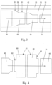
- Fig. 3 shows a charge transfer channel in plan view.
- the conduction layer 30 is embedded in the semiconductor substrate 20.
- the insulation layer above it is not shown.
- the gates 40, 50, 41 are arranged in the flow direction 31 of the electrons and electrically separated at distances 42. Overall, the gates show a narrowing of the cross-section in the flow direction.
- the first gate 40 has a wide cross-section, while the last gate 41 has a comparatively narrower cross-section.
- the two gates 50 have a cross-section that narrows in the flow direction 31.
- the narrowing gate 50 initially has a wide area with a constant cross-section without a constriction 51 in the flow direction 31, then an area with a narrower cross-section and a constriction 52, and then a narrower area with a constant cross-section again and without a constriction 51.
- the gate 50 has areas with a constant cross-section at the transition to the neighboring gates.
- the area with a constant cross-section and without a constriction arranged against the flow direction is shorter than the area with a constant cross-section and without a constriction arranged in the flow direction.
- the narrowing area with a constriction 52 is shifted from the center of the gate 50 against the direction of the flow.
- the narrowing area with a constriction 52 is beveled on both sides so that it has a funnel shape.
- the design of a constriction shown in this way can minimize the spillback and/or the flow resistance and/or the losses of the charge carriers in the flow direction.
- Fig. 4 shows the gates of a charge transfer channel in plan view.
- the conduction layer located under the gates is not shown.
- the maximum width of the gates 40 located in the flow direction at the beginning and end of the gate sequence shown forms the typical width of the cross section of the conduction transfer channel.
- the two gates 60 have a connected area of a bulge 61 in which the cross section is increased by about 25% by the width 62 compared to the typical width.
- the first gate 60 with the bulge has a constriction 62 in which the cross section of the charge transfer channel is narrower compared to the typical width.
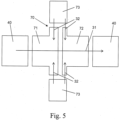
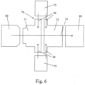
- Fig. 6 shows the arrangement of Figure 5 , the first gate 50 having a constriction. Due to the design of a mouth area shown in this way, the Spill back and/or flow resistance and/or charge carrier losses in the flow direction can be further minimized.
Landscapes
- Solid State Image Pick-Up Elements (AREA)
Claims (4)
- Dispositif de transfert de charge, comprenant- un canal de transfert de charge dans un substrat semi-conducteur,- une couche conductrice dopée- pour recevoir les porteurs de charge de manière mobile,- une série d'au moins deux grilles électriquement isolées- qui se suivent en étant voisines- pour décaler les porteurs de charge dans la couche conductrice- dans une direction de flux,- dans lequel le canal de transfert de charge est réalisé par le chevauchement de l'effet électrostatique possible des grilles avec la couche conductrice, et- un générateur d'horloge- ayant une fréquence d'horloge de plus de 100 Mhz, de préférence de plus de 150 Mhz, de plus de 200 Mhz ou de plus de 250 Mhz, et de manière particulièrement préférée jusqu'à 300 Mhz ou 400 MHz,- qui soumet les grilles à des changements de potentiel à la fréquence d'horloge- pour transporter des porteurs de charge à la fréquence d'horloge à partir de zones voisines du chevauchement de grilles voisines avec la couche conductrice jusqu'à des zones voisines du chevauchement de grilles voisines avec la couche conductrice,dans lequel- le canal de transfert de charge présente une zone d'embouchure- qui est disposée dans la direction de flux à une limite extérieure latérale du canal de transfert de charge, et- qui s'étend au moins en partie sur les zones d'exactement deux grilles voisines du canal de transmission de charge- afin d'acheminer des porteurs de charge au canal de transfert de charge à partir d'une zone adjacente à la zone d'embouchure à l'extérieur du canal de transfert de charge, en particulier à partir d'un deuxième canal de transfert de charge, et- pour réduire le retour ou la résistance au flux ou la perte des porteurs de charge dans la direction de flux du canal de transfert de charge ou de la zone acheminant des porteurs de charge au canal de transfert de charge, de préférence d'un deuxième canal de transfert de charge, dans lequel- la longueur de la zone d'embouchure le long du canal de conduction- est inférieure à la longueur de la zone des deux grilles voisines associées le long du canal de transfert de charge, et- de 45 à 75 % ou de 55 à 65 % ou 60 % correspondent à la longueur de la zone des deux grilles voisines associées le long du canal de transfert de charge, dans lequel- la zone d'embouchure est adjacente de manière décalée- par sa longueur le long du canal de transfert de conduction- sur une plus grande longueur à la zone de la grille associée située à l'opposé de la direction de flux qu'à la zone de la grille associée située dans la direction de flux, dans lequel les grilles sont disposées de manière électriquement isolée à intervalles, et- est adjacente de préférence à plus de 50 %, plus de 60 %, entre 60 % et 75 % ou à 2/3 à la zone de la grille associée située à l'opposé de la direction de flux.
- Dispositif de transfert de charge selon la revendication 1,
dans lequel- la zone d'embouchure comprenant- une échancrure- dans laquelle la section transversale par rapport à la direction de flux augmente d'abord, de préférence de plus de 20 %, 40 %, 80 % ou 100 %, et diminue ensuite à nouveau, de préférence de plus de 20 %, 40 % ou 80 %,- qui s'étend dans sa longueur dans la direction de flux au moins ou exactement sur la zone d'embouchure,- dans lequel la longueur de l'échancrure dans la direction de flux est inférieure à la largeur de l'augmentation de la section transversale, de préférence inférieure à 50 %, inférieure à 25 % ou inférieure à 12 %,- dans lequel l'échancrure est de préférence rectangulaire. - Dispositif de transfert de charge selon l'une quelconque des revendications précédentes,
dans lequel- le canal de transfert de charge présente une zone d'un rétrécissement- dans laquelle la section transversale diminue dans la direction de flux, et- qui est disposée à l'opposé de la direction de flux en amont du point d'embouchure, et- au moins partiellement dans la zone de ladite une grille associée située à l'opposé de la direction de flux, et- est réalisée de préférence de manière chanfreinée et/ou en forme d'entonnoir- afin de réduire le retour ou la résistance au flux ou la perte des porteurs de charge dans la direction de flux. - Dispositif de transfert de charge selon l'une quelconque des revendications précédentes,
dans lequel- le substrat semi-conducteur est dopé p+, et/ou- la couche conductrice est faiblement dopée n-, et/ou- les grilles sont formées en métal, et/ou- une couche non conductrice est disposée entre les grilles et la couche conductrice.
Priority Applications (3)
| Application Number | Priority Date | Filing Date | Title |
|---|---|---|---|
| EP21189012.4A EP4131382B1 (fr) | 2021-08-02 | 2021-08-02 | Dispositif de transfert de charge doté d'une zone d'ouverture pour fréquences d'horloge à partir de 100 mhz |
| US18/293,656 US20240339529A1 (en) | 2021-08-02 | 2022-07-29 | Charge transfer device having an influx portion for clock frequencies from 100 MHz |
| PCT/EP2022/071379 WO2023012066A1 (fr) | 2021-08-02 | 2022-07-29 | Dispositif de transfert de charge comprenant une partie de flux entrant pour des fréquences d'horloge à partir de 100 mhz |
Applications Claiming Priority (1)
| Application Number | Priority Date | Filing Date | Title |
|---|---|---|---|
| EP21189012.4A EP4131382B1 (fr) | 2021-08-02 | 2021-08-02 | Dispositif de transfert de charge doté d'une zone d'ouverture pour fréquences d'horloge à partir de 100 mhz |
Publications (2)
| Publication Number | Publication Date |
|---|---|
| EP4131382A1 EP4131382A1 (fr) | 2023-02-08 |
| EP4131382B1 true EP4131382B1 (fr) | 2025-02-26 |
Family
ID=77168055
Family Applications (1)
| Application Number | Title | Priority Date | Filing Date |
|---|---|---|---|
| EP21189012.4A Active EP4131382B1 (fr) | 2021-08-02 | 2021-08-02 | Dispositif de transfert de charge doté d'une zone d'ouverture pour fréquences d'horloge à partir de 100 mhz |
Country Status (3)
| Country | Link |
|---|---|
| US (1) | US20240339529A1 (fr) |
| EP (1) | EP4131382B1 (fr) |
| WO (1) | WO2023012066A1 (fr) |
Families Citing this family (1)
| Publication number | Priority date | Publication date | Assignee | Title |
|---|---|---|---|---|
| EP4131384A1 (fr) * | 2021-08-02 | 2023-02-08 | Espros Photonics AG | Dispositif de transfert de charge pourvu de rétrécissement sur le grillage pour les fréquences d'horloge à partir de 100 mhz |
Family Cites Families (3)
| Publication number | Priority date | Publication date | Assignee | Title |
|---|---|---|---|---|
| JP3649397B2 (ja) * | 2002-03-01 | 2005-05-18 | 松下電器産業株式会社 | 固体撮像装置およびその製造方法 |
| JP4967237B2 (ja) * | 2005-01-28 | 2012-07-04 | パナソニック株式会社 | 固体撮像装置 |
| GB2551108A (en) * | 2016-05-06 | 2017-12-13 | Teledyne E2V (Uk) Ltd | Image sensor |
-
2021
- 2021-08-02 EP EP21189012.4A patent/EP4131382B1/fr active Active
-
2022
- 2022-07-29 WO PCT/EP2022/071379 patent/WO2023012066A1/fr not_active Ceased
- 2022-07-29 US US18/293,656 patent/US20240339529A1/en active Pending
Also Published As
| Publication number | Publication date |
|---|---|
| EP4131382A1 (fr) | 2023-02-08 |
| WO2023012066A1 (fr) | 2023-02-09 |
| US20240339529A1 (en) | 2024-10-10 |
Similar Documents
| Publication | Publication Date | Title |
|---|---|---|
| DE69523192T2 (de) | Halbleiterbauelement mit isoliertem Gate und Verfahren zu dessen Herstellung | |
| DE102013206900B4 (de) | Halbleiterbauelement mit kernlosem Übertrager und Verfahren zum Betrieb eines solchen Halbleiterbauelements | |
| EP1200970B1 (fr) | Varistor multicouche de faible capacite | |
| DE60034483T2 (de) | L- und U-Gate-Bauelemente für SOI/SOS-Anwendungen | |
| DE10132136C1 (de) | Halbleiterbauelement mit Ladungskompensationsstruktur sowie zugehöriges Herstellungsverfahren | |
| DE69418365T2 (de) | Hochspannung-MIS-Feldeffekttransistor | |
| DE19541497B4 (de) | Lateraler Feldeffekttransistor | |
| DE1764164B1 (de) | Sperrschicht feldeffektransistor | |
| DE102007024112A1 (de) | Halbleitervorrichtung mit isoliertem Gate | |
| DE1614144A1 (de) | Feldeffekttransistor mit isolierten Gattern | |
| EP4131382B1 (fr) | Dispositif de transfert de charge doté d'une zone d'ouverture pour fréquences d'horloge à partir de 100 mhz | |
| EP4131383B1 (fr) | Dispositif de transfert de charge doté d'une zone de courbure pour fréquences d'horloge à partir de 100 mhz | |
| DE102014203851B4 (de) | Schaltungsanordnung | |
| DE102019200116A1 (de) | Halbleitervorrichtung | |
| WO2025119822A1 (fr) | Composant inductif | |
| WO2023012068A1 (fr) | Dispositif de transfert de charge ayant une conicité au niveau de la grille pour des fréquences d'horloge à partir de 100 mhz | |
| DE102018213735B4 (de) | Bauelement und Verfahren zum Herstellen eines Bauelements | |
| DE102007020249B4 (de) | Halbleiterbauelement, Halbleitersensorstruktur sowie Vorrichtung und Verfahren zum Herstellen eines Halbleiterbauelement | |
| EP1001481A2 (fr) | Coupleur interdigital intégré monolithiquement | |
| DE3782485T2 (de) | Isolierender abstandshalter fuer gasisoliertes elektrisches geraet. | |
| EP3338321B1 (fr) | Antenne double bande | |
| EP1186052B1 (fr) | Transistor de puissance dont la source est situee sur la face inferieure | |
| DE112017007966T5 (de) | Feldeffekttransistor | |
| EP3591088B1 (fr) | Dispositif de revêtement par immersion à chaud d'une bande métallique | |
| DE102017125803B4 (de) | Halbleiterbauelement mit einer Transistorstruktur vom Anreicherungstyp |
Legal Events
| Date | Code | Title | Description |
|---|---|---|---|
| PUAI | Public reference made under article 153(3) epc to a published international application that has entered the european phase |
Free format text: ORIGINAL CODE: 0009012 |
|
| STAA | Information on the status of an ep patent application or granted ep patent |
Free format text: STATUS: THE APPLICATION HAS BEEN PUBLISHED |
|
| AK | Designated contracting states |
Kind code of ref document: A1 Designated state(s): AL AT BE BG CH CY CZ DE DK EE ES FI FR GB GR HR HU IE IS IT LI LT LU LV MC MK MT NL NO PL PT RO RS SE SI SK SM TR |
|
| P01 | Opt-out of the competence of the unified patent court (upc) registered |
Effective date: 20230523 |
|
| STAA | Information on the status of an ep patent application or granted ep patent |
Free format text: STATUS: REQUEST FOR EXAMINATION WAS MADE |
|
| 17P | Request for examination filed |
Effective date: 20230726 |
|
| RBV | Designated contracting states (corrected) |
Designated state(s): AL AT BE BG CH CY CZ DE DK EE ES FI FR GB GR HR HU IE IS IT LI LT LU LV MC MK MT NL NO PL PT RO RS SE SI SK SM TR |
|
| GRAP | Despatch of communication of intention to grant a patent |
Free format text: ORIGINAL CODE: EPIDOSNIGR1 |
|
| STAA | Information on the status of an ep patent application or granted ep patent |
Free format text: STATUS: GRANT OF PATENT IS INTENDED |
|
| INTG | Intention to grant announced |
Effective date: 20241031 |
|
| RIN1 | Information on inventor provided before grant (corrected) |
Inventor name: YU, CHONGQI Inventor name: DE COI, BEAT |
|
| GRAS | Grant fee paid |
Free format text: ORIGINAL CODE: EPIDOSNIGR3 |
|
| GRAA | (expected) grant |
Free format text: ORIGINAL CODE: 0009210 |
|
| STAA | Information on the status of an ep patent application or granted ep patent |
Free format text: STATUS: THE PATENT HAS BEEN GRANTED |
|
| AK | Designated contracting states |
Kind code of ref document: B1 Designated state(s): AL AT BE BG CH CY CZ DE DK EE ES FI FR GB GR HR HU IE IS IT LI LT LU LV MC MK MT NL NO PL PT RO RS SE SI SK SM TR |
|
| REG | Reference to a national code |
Ref country code: GB Ref legal event code: FG4D Free format text: NOT ENGLISH |
|
| REG | Reference to a national code |
Ref country code: DE Ref legal event code: R096 Ref document number: 502021006762 Country of ref document: DE |
|
| REG | Reference to a national code |
Ref country code: IE Ref legal event code: FG4D Free format text: LANGUAGE OF EP DOCUMENT: GERMAN |
|
| REG | Reference to a national code |
Ref country code: NL Ref legal event code: MP Effective date: 20250226 |
|
| PG25 | Lapsed in a contracting state [announced via postgrant information from national office to epo] |
Ref country code: RS Free format text: LAPSE BECAUSE OF FAILURE TO SUBMIT A TRANSLATION OF THE DESCRIPTION OR TO PAY THE FEE WITHIN THE PRESCRIBED TIME-LIMIT Effective date: 20250526 |
|
| PG25 | Lapsed in a contracting state [announced via postgrant information from national office to epo] |
Ref country code: FI Free format text: LAPSE BECAUSE OF FAILURE TO SUBMIT A TRANSLATION OF THE DESCRIPTION OR TO PAY THE FEE WITHIN THE PRESCRIBED TIME-LIMIT Effective date: 20250226 |
|
| PG25 | Lapsed in a contracting state [announced via postgrant information from national office to epo] |
Ref country code: PL Free format text: LAPSE BECAUSE OF FAILURE TO SUBMIT A TRANSLATION OF THE DESCRIPTION OR TO PAY THE FEE WITHIN THE PRESCRIBED TIME-LIMIT Effective date: 20250226 |
|
| PG25 | Lapsed in a contracting state [announced via postgrant information from national office to epo] |
Ref country code: ES Free format text: LAPSE BECAUSE OF FAILURE TO SUBMIT A TRANSLATION OF THE DESCRIPTION OR TO PAY THE FEE WITHIN THE PRESCRIBED TIME-LIMIT Effective date: 20250226 |
|
| REG | Reference to a national code |
Ref country code: LT Ref legal event code: MG9D |
|
| PG25 | Lapsed in a contracting state [announced via postgrant information from national office to epo] |
Ref country code: NO Free format text: LAPSE BECAUSE OF FAILURE TO SUBMIT A TRANSLATION OF THE DESCRIPTION OR TO PAY THE FEE WITHIN THE PRESCRIBED TIME-LIMIT Effective date: 20250526 Ref country code: IS Free format text: LAPSE BECAUSE OF FAILURE TO SUBMIT A TRANSLATION OF THE DESCRIPTION OR TO PAY THE FEE WITHIN THE PRESCRIBED TIME-LIMIT Effective date: 20250626 |
|
| PG25 | Lapsed in a contracting state [announced via postgrant information from national office to epo] |
Ref country code: NL Free format text: LAPSE BECAUSE OF FAILURE TO SUBMIT A TRANSLATION OF THE DESCRIPTION OR TO PAY THE FEE WITHIN THE PRESCRIBED TIME-LIMIT Effective date: 20250226 |
|
| PG25 | Lapsed in a contracting state [announced via postgrant information from national office to epo] |
Ref country code: HR Free format text: LAPSE BECAUSE OF FAILURE TO SUBMIT A TRANSLATION OF THE DESCRIPTION OR TO PAY THE FEE WITHIN THE PRESCRIBED TIME-LIMIT Effective date: 20250226 |
|
| PG25 | Lapsed in a contracting state [announced via postgrant information from national office to epo] |
Ref country code: LV Free format text: LAPSE BECAUSE OF FAILURE TO SUBMIT A TRANSLATION OF THE DESCRIPTION OR TO PAY THE FEE WITHIN THE PRESCRIBED TIME-LIMIT Effective date: 20250226 Ref country code: PT Free format text: LAPSE BECAUSE OF FAILURE TO SUBMIT A TRANSLATION OF THE DESCRIPTION OR TO PAY THE FEE WITHIN THE PRESCRIBED TIME-LIMIT Effective date: 20250626 |
|
| PG25 | Lapsed in a contracting state [announced via postgrant information from national office to epo] |
Ref country code: BG Free format text: LAPSE BECAUSE OF FAILURE TO SUBMIT A TRANSLATION OF THE DESCRIPTION OR TO PAY THE FEE WITHIN THE PRESCRIBED TIME-LIMIT Effective date: 20250226 Ref country code: GR Free format text: LAPSE BECAUSE OF FAILURE TO SUBMIT A TRANSLATION OF THE DESCRIPTION OR TO PAY THE FEE WITHIN THE PRESCRIBED TIME-LIMIT Effective date: 20250527 |
|
| PG25 | Lapsed in a contracting state [announced via postgrant information from national office to epo] |
Ref country code: SE Free format text: LAPSE BECAUSE OF FAILURE TO SUBMIT A TRANSLATION OF THE DESCRIPTION OR TO PAY THE FEE WITHIN THE PRESCRIBED TIME-LIMIT Effective date: 20250226 |
|
| PG25 | Lapsed in a contracting state [announced via postgrant information from national office to epo] |
Ref country code: SM Free format text: LAPSE BECAUSE OF FAILURE TO SUBMIT A TRANSLATION OF THE DESCRIPTION OR TO PAY THE FEE WITHIN THE PRESCRIBED TIME-LIMIT Effective date: 20250226 |
|
| PG25 | Lapsed in a contracting state [announced via postgrant information from national office to epo] |
Ref country code: DK Free format text: LAPSE BECAUSE OF FAILURE TO SUBMIT A TRANSLATION OF THE DESCRIPTION OR TO PAY THE FEE WITHIN THE PRESCRIBED TIME-LIMIT Effective date: 20250226 |
|
| PGFP | Annual fee paid to national office [announced via postgrant information from national office to epo] |
Ref country code: DE Payment date: 20250819 Year of fee payment: 5 |
|
| PG25 | Lapsed in a contracting state [announced via postgrant information from national office to epo] |
Ref country code: IT Free format text: LAPSE BECAUSE OF FAILURE TO SUBMIT A TRANSLATION OF THE DESCRIPTION OR TO PAY THE FEE WITHIN THE PRESCRIBED TIME-LIMIT Effective date: 20250226 |
|
| PGFP | Annual fee paid to national office [announced via postgrant information from national office to epo] |
Ref country code: AT Payment date: 20251020 Year of fee payment: 5 |
|
| PG25 | Lapsed in a contracting state [announced via postgrant information from national office to epo] |
Ref country code: CZ Free format text: LAPSE BECAUSE OF FAILURE TO SUBMIT A TRANSLATION OF THE DESCRIPTION OR TO PAY THE FEE WITHIN THE PRESCRIBED TIME-LIMIT Effective date: 20250226 Ref country code: EE Free format text: LAPSE BECAUSE OF FAILURE TO SUBMIT A TRANSLATION OF THE DESCRIPTION OR TO PAY THE FEE WITHIN THE PRESCRIBED TIME-LIMIT Effective date: 20250226 |
|
| PG25 | Lapsed in a contracting state [announced via postgrant information from national office to epo] |
Ref country code: RO Free format text: LAPSE BECAUSE OF FAILURE TO SUBMIT A TRANSLATION OF THE DESCRIPTION OR TO PAY THE FEE WITHIN THE PRESCRIBED TIME-LIMIT Effective date: 20250226 |
|
| PG25 | Lapsed in a contracting state [announced via postgrant information from national office to epo] |
Ref country code: SK Free format text: LAPSE BECAUSE OF FAILURE TO SUBMIT A TRANSLATION OF THE DESCRIPTION OR TO PAY THE FEE WITHIN THE PRESCRIBED TIME-LIMIT Effective date: 20250226 |
|
| REG | Reference to a national code |
Ref country code: DE Ref legal event code: R097 Ref document number: 502021006762 Country of ref document: DE |
|
| PLBE | No opposition filed within time limit |
Free format text: ORIGINAL CODE: 0009261 |
|
| STAA | Information on the status of an ep patent application or granted ep patent |
Free format text: STATUS: NO OPPOSITION FILED WITHIN TIME LIMIT |
|
| REG | Reference to a national code |
Ref country code: CH Ref legal event code: L10 Free format text: ST27 STATUS EVENT CODE: U-0-0-L10-L00 (AS PROVIDED BY THE NATIONAL OFFICE) Effective date: 20260107 |
|
| 26N | No opposition filed |
Effective date: 20251127 |
|
| REG | Reference to a national code |
Ref country code: CH Ref legal event code: H13 Free format text: ST27 STATUS EVENT CODE: U-0-0-H10-H13 (AS PROVIDED BY THE NATIONAL OFFICE) Effective date: 20260324 |
|
| PG25 | Lapsed in a contracting state [announced via postgrant information from national office to epo] |
Ref country code: MC Free format text: LAPSE BECAUSE OF FAILURE TO SUBMIT A TRANSLATION OF THE DESCRIPTION OR TO PAY THE FEE WITHIN THE PRESCRIBED TIME-LIMIT Effective date: 20250226 |
|
| PG25 | Lapsed in a contracting state [announced via postgrant information from national office to epo] |
Ref country code: LU Free format text: LAPSE BECAUSE OF NON-PAYMENT OF DUE FEES Effective date: 20250802 |
|
| PG25 | Lapsed in a contracting state [announced via postgrant information from national office to epo] |
Ref country code: CH Free format text: LAPSE BECAUSE OF NON-PAYMENT OF DUE FEES Effective date: 20250831 |