EP4131385A1 - Structure empilée, écran d'affichage et dispositif d'affichage - Google Patents
Structure empilée, écran d'affichage et dispositif d'affichage Download PDFInfo
- Publication number
- EP4131385A1 EP4131385A1 EP21797561.4A EP21797561A EP4131385A1 EP 4131385 A1 EP4131385 A1 EP 4131385A1 EP 21797561 A EP21797561 A EP 21797561A EP 4131385 A1 EP4131385 A1 EP 4131385A1
- Authority
- EP
- European Patent Office
- Prior art keywords
- drive chip
- layer
- pixel
- sub
- stacked structure
- Prior art date
- Legal status (The legal status is an assumption and is not a legal conclusion. Google has not performed a legal analysis and makes no representation as to the accuracy of the status listed.)
- Pending
Links
Images



Classifications
-
- G—PHYSICS
- G09—EDUCATION; CRYPTOGRAPHY; DISPLAY; ADVERTISING; SEALS
- G09G—ARRANGEMENTS OR CIRCUITS FOR CONTROL OF INDICATING DEVICES USING STATIC MEANS TO PRESENT VARIABLE INFORMATION
- G09G3/00—Control arrangements or circuits, of interest only in connection with visual indicators other than cathode-ray tubes
- G09G3/20—Control arrangements or circuits, of interest only in connection with visual indicators other than cathode-ray tubes for presentation of an assembly of a number of characters, e.g. a page, by composing the assembly by combination of individual elements arranged in a matrix no fixed position being assigned to or needed to be assigned to the individual characters or partial characters
- G09G3/22—Control arrangements or circuits, of interest only in connection with visual indicators other than cathode-ray tubes for presentation of an assembly of a number of characters, e.g. a page, by composing the assembly by combination of individual elements arranged in a matrix no fixed position being assigned to or needed to be assigned to the individual characters or partial characters using controlled light sources
- G09G3/30—Control arrangements or circuits, of interest only in connection with visual indicators other than cathode-ray tubes for presentation of an assembly of a number of characters, e.g. a page, by composing the assembly by combination of individual elements arranged in a matrix no fixed position being assigned to or needed to be assigned to the individual characters or partial characters using controlled light sources using electroluminescent panels
- G09G3/32—Control arrangements or circuits, of interest only in connection with visual indicators other than cathode-ray tubes for presentation of an assembly of a number of characters, e.g. a page, by composing the assembly by combination of individual elements arranged in a matrix no fixed position being assigned to or needed to be assigned to the individual characters or partial characters using controlled light sources using electroluminescent panels semiconductive, e.g. using light-emitting diodes [LED]
-
- H—ELECTRICITY
- H10—SEMICONDUCTOR DEVICES; ELECTRIC SOLID-STATE DEVICES NOT OTHERWISE PROVIDED FOR
- H10H—INORGANIC LIGHT-EMITTING SEMICONDUCTOR DEVICES HAVING POTENTIAL BARRIERS
- H10H20/00—Individual inorganic light-emitting semiconductor devices having potential barriers, e.g. light-emitting diodes [LED]
- H10H20/80—Constructional details
- H10H20/83—Electrodes
-
- H—ELECTRICITY
- H10—SEMICONDUCTOR DEVICES; ELECTRIC SOLID-STATE DEVICES NOT OTHERWISE PROVIDED FOR
- H10H—INORGANIC LIGHT-EMITTING SEMICONDUCTOR DEVICES HAVING POTENTIAL BARRIERS
- H10H20/00—Individual inorganic light-emitting semiconductor devices having potential barriers, e.g. light-emitting diodes [LED]
- H10H20/80—Constructional details
- H10H20/85—Packages
- H10H20/8506—Containers
-
- H—ELECTRICITY
- H10—SEMICONDUCTOR DEVICES; ELECTRIC SOLID-STATE DEVICES NOT OTHERWISE PROVIDED FOR
- H10H—INORGANIC LIGHT-EMITTING SEMICONDUCTOR DEVICES HAVING POTENTIAL BARRIERS
- H10H20/00—Individual inorganic light-emitting semiconductor devices having potential barriers, e.g. light-emitting diodes [LED]
- H10H20/80—Constructional details
- H10H20/85—Packages
- H10H20/852—Encapsulations
-
- H—ELECTRICITY
- H10—SEMICONDUCTOR DEVICES; ELECTRIC SOLID-STATE DEVICES NOT OTHERWISE PROVIDED FOR
- H10H—INORGANIC LIGHT-EMITTING SEMICONDUCTOR DEVICES HAVING POTENTIAL BARRIERS
- H10H20/00—Individual inorganic light-emitting semiconductor devices having potential barriers, e.g. light-emitting diodes [LED]
- H10H20/80—Constructional details
- H10H20/85—Packages
- H10H20/857—Interconnections, e.g. lead-frames, bond wires or solder balls
-
- H—ELECTRICITY
- H10—SEMICONDUCTOR DEVICES; ELECTRIC SOLID-STATE DEVICES NOT OTHERWISE PROVIDED FOR
- H10H—INORGANIC LIGHT-EMITTING SEMICONDUCTOR DEVICES HAVING POTENTIAL BARRIERS
- H10H29/00—Integrated devices, or assemblies of multiple devices, comprising at least one light-emitting semiconductor element covered by group H10H20/00
- H10H29/10—Integrated devices comprising at least one light-emitting semiconductor component covered by group H10H20/00
- H10H29/14—Integrated devices comprising at least one light-emitting semiconductor component covered by group H10H20/00 comprising multiple light-emitting semiconductor components
- H10H29/142—Two-dimensional arrangements, e.g. asymmetric LED layout
-
- H—ELECTRICITY
- H10—SEMICONDUCTOR DEVICES; ELECTRIC SOLID-STATE DEVICES NOT OTHERWISE PROVIDED FOR
- H10W—GENERIC PACKAGES, INTERCONNECTIONS, CONNECTORS OR OTHER CONSTRUCTIONAL DETAILS OF DEVICES COVERED BY CLASS H10
- H10W90/00—Package configurations
-
- G—PHYSICS
- G09—EDUCATION; CRYPTOGRAPHY; DISPLAY; ADVERTISING; SEALS
- G09G—ARRANGEMENTS OR CIRCUITS FOR CONTROL OF INDICATING DEVICES USING STATIC MEANS TO PRESENT VARIABLE INFORMATION
- G09G2300/00—Aspects of the constitution of display devices
- G09G2300/04—Structural and physical details of display devices
- G09G2300/0421—Structural details of the set of electrodes
- G09G2300/0426—Layout of electrodes and connections
Definitions
- This application provides a stacked structure, a display screen, and a display apparatus, to improve a display effect of the display screen.
- the P pole, the light-emitting layer, and the N pole are stacked, and the light-emitting layer is located between the P pole and the N pole.
- a volume of the sub-pixel is reduced by using the stacked structure.
- the P pole, the light-emitting layer, and the N pole are stacked, and the P pole and the N pole are disposed on a same layer. Power is supplied in a horizontal direction.
- a material of the substrate may be glass, silicon, sapphire, or PI (polyimide, which is a polymer containing an imide group in the main chain).
- the line layer 50 is stacked with the substrate and is connected to the drive chip 20 and the pixel unit 30.
- the line layer 50 is further connected to the DDIC to implement electrical connection between the DDIC and the light-emitting unit.
- the drive chip 20 is disposed on the substrate.
- the substrate shown in FIG. 2 carries a drive chip 20.
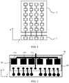
- the drive chip 20 is of a rectangular shape, and a length direction of the drive chip 20 is arranged in the direction a.
- the drive chip 20 may be a micro integrated circuit (Micro Integrated circuit, ⁇ IC).
- a quantity of the drive chips 20 carried on the substrate is not specifically limited.
- the substrate may further carry two, three, four, or five drive chips 20.
- all stacked structures in the display screen may share one substrate.
- the drive chips 20 in the display screen are arranged in arrays on the substrate, and the drive chips 20 are electrically connected to the substrate, and are connected to the DDIC through the substrate.
- a pixel unit 30 is disposed in the drive chip 20.
- the drive chip 20 shown in FIG. 2 carries two pixel units 30, and the two pixel units 30 are arranged in a direction a.
- a quantity of pixel units 30 carried on the drive chip 20 is not limited in this embodiment of this application.
- the drive chip 20 may carry a different quantity of pixel units 30, for example, one pixel unit 30, three pixel units 30, or four pixel units 30.
- the drive chip 20 carries a plurality of pixel units 30, the plurality of pixel units 30 are arranged in a single row in the direction a.
- Each pixel unit 30 includes three sub-pixels disposed at a same layer, and the three sub-pixels are arranged in a single row in the direction a.
- the three sub-pixels are respectively sub-pixels that can emit red, blue, and green colors.
- the three sub-pixels shown in FIG. 2 are respectively a first sub-pixel 31a that can emit red light, a second sub-pixel 31b that can emit blue light, and a third sub-pixel 31c that can emit green light.
- the drive chip 20 can control the pixel unit 30 to emit light of different colors by controlling working statuses of the three sub-pixels.
- the pixel unit 30 may further include other sub-pixels that can meet a requirement that the display screen emits light of different colors, for example, sub-pixels using a monochrome, or sub-pixels using three colors R, G, and B.
- a quantity of sub-pixels in each pixel unit 30 and a color of light emitted by each sub-pixel are not specifically limited.
- the sub-pixel may be set based on a requirement.
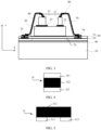
- FIG. 3 is a side view of the stacked structure shown in FIG. 2 , and may directly reflect a specific stacking situation of the stacked structure provided in this embodiment of this application.
- a direction z is defined.
- the direction z is a direction that is directed from the inside of a display screen to a display surface of the display screen.
- a substrate 10, a drive chip 20, and a pixel unit are stacked to form a three-layer structure along the direction z, and the pixel unit is close to the display surface of the display screen.
- the substrate 10 has a first surface, a line layer 50 is disposed on the first surface, and the line layer 50 has a circuit layer 52 that connects a DDIC, the drive chip 20, and a sub-pixel 31.
- the line layer 50 shown in FIG. 3 includes a support layer 51 and the circuit layer 52, and the support layer 51 may use different materials.
- a material of the line layer 50 may be PI or epoxy resin.
- the circuit layer 52 may be used to perform multilayer wiring inside the support layer 51, or may be used to perform wiring on a surface of the line layer 50.
- the circuit layer 52 may be directly disposed on the substrate 10, and the substrate 10 is used as a support structure of the circuit layer 52, so that no additional support layer 51 needs to be prepared to support the circuit layer 52.
- a printed circuit board or a substrate with a circuit is used.
- the drive chip 20 is disposed on the surface that is of the line layer 50 and that faces away from the first surface. Specifically, the drive chip 20 may be fixed to the surface of the line layer 50 through film adhesion, metallic bonding, or paste material adhesion.
- the drive chip 20 has a binding post 21.
- the binding post 21 is disposed on the surface that is of the drive chip 20 and that faces away from the line layer 50, and the binding post 21 is electrically connected to the circuit layer 52. Specifically, the binding post 21 is connected to an IO pad 22 of the drive chip 20 by using a connection wire 70.
- the binding post 21 may be connected to an IO (Input Output, electrical signal input/output) pad 54 of the line layer 50 by using an RDL (redistribution Redistribution Layer), or may be connected to the IO pad 54 of the line layer 50 by using a fanout (fanout) line, to implement electrical connection between the drive chip 20 and the circuit layer 52.
- a material of the connection wire 70 may be conductive materials, such as Cu pillar (copper pillar bump), ITO (Information Technology Outsourcing, indium tin oxide), Cu, or Au.
- a sub-pixel 31 located in each pixel unit is separately electrically connected to the line layer 50 and a corresponding drive chip 20 to form a light-emitting loop.
- the sub-pixel 31 is assembled on the surface of the drive chip 20 (the surface that faces away from the first surface) by using a transfer process and a bonding (bonding) process.
- the sub-pixel corresponding to each drive chip is disposed on the surface that is of a corresponding drive chip and that faces away from the line 50.
- Vertical projections of a plurality of sub-pixels on the first surface are located in a vertical projection of the drive chip on the first surface.
- the foregoing correspondence is a correspondence between the drive chip and the sub-pixel for forming an electrical connection loop.
- the sub-pixel 31 may use a micro light-emitting diode (Micro Light-emitting diode, ⁇ LED).
- the sub-pixel 31 provided in this embodiment of this application includes a light-emitting layer 312, and a P pole 313 and an N pole 311 that are separately connected to the light-emitting layer 312.
- the P pole 313, the light-emitting layer 312, and the N pole 311 of the sub-pixel 31 are stacked, and the light-emitting layer 312 is located between the P pole 313 and the N pole 311.
- the P pole 313 of the sub-pixel 31 is connected to the P pad 23 of the drive chip.
- the N pole 311 of the sub-pixel 31 is connected to the GND pad 53 of the line layer 50 by using a connection wire 60.
- the N pole 311 of the sub-pixel 31 may be connected to the GND pad 53 of the line layer 50 by using an RDL, or may be connected to the GND pad 53 of the line layer 50 by using a fanout line, to implement electrical connection between the sub-pixel 31 and the circuit layer 52.
- a material of the connection wire 60 may be conductive materials, such as Cu pillar, ITO, Cu, or Au.
- the drive chip 20 and the sub-pixel 31 are connected to corresponding poles (a GND pad 53 and an IO pad 54) of the drive chip 20 and the sub-pixel 31 on the circuit layer 52 by using the RDL process or the fanout process, to implement a circuit loop of the entire stacked structure.
- the sub-pixel may be connected to the IO pad of the circuit layer, and the IO pad of the drive chip may be connected to the GND pad of the circuit layer.
- the drive chip and the sub-pixel may be electrically connected to the circuit layer.
- an area in which the drive chip 20 is disposed on the line layer 50 is insulated from the drive chip 20.
- the drive chip 20 is fixed to the line layer 50, no circuit is disposed in an area covered by the drive chip 20.
- inner layer wiring is not arranged in the area in which the drive chip 20 is disposed on the line layer 50.
- a first area 53 is the area that covers the drive chip 20 when the drive chip 20 is disposed on the line layer 50. It can be learned from FIG. 3 that, when the light-emitting unit is separated by using the separation layer, the line layer 50 connected to the light-emitting unit needs to be separated together.
- the stacked structure further includes a second packaging layer 80 corresponding to each drive chip 20, and each second packaging layer 80 packages a corresponding drive chip 20 and the plurality of sub-pixels 31 to protect the drive chip 20 and the sub-pixels 31.
- the second packaging layer 80 is of a trapezoidal structure, and wraps the drive chip 20 and the sub-pixels 31.
- the second packaging layer 80 is made of a transparent plastic packaging material, so that light emitted by the sub-pixels 31 can penetrate through.
- a material of the second packaging layer 80 may be a COF (Chip On Flex, or, Chip On Film, chip on film) material, may be a transparent photoresist material, or may be another transparent epoxy resin material.
- connection wire that connects the drive chip 20 and the sub-pixels 31 to the circuit layer may be disposed in the second packaging layer 80, and the second packaging layer 80 is used to package the connection wire together with the drive chip 20 and the sub-pixels 31.
- the connection wire may be attached to a surface of the second packaging layer 80.
- the binding post 21 may be disposed on the second packaging layer 80 by using a metallic via, or by using a column structure.
- a via may be provided in the second packaging layer 80.
- the via may be plated with a metal layer to form a metallic via, which is used as the binding post, or the via may be filled with a metal material to form a column structure, which is used as the binding post.
- the stacked structure provided in this embodiment of this application is formed by stacking the drive chip and the pixel unit, an area occupied by the light-emitting unit on the substrate can be effectively reduced.
- the stacked structure provided in this embodiment of this application is compared with a stacked structure in the conventional technology.
- the following describes the stacked structure in this application and the stacked structure in the conventional technology with reference to FIG. 6 and FIG. 7 .
- a comparison in a length direction is used to describe differences between the two stacked structures.
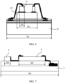
- FIG. 6 is a side view of a stacked structure according to an embodiment of this application.
- a length of the substrate 10 is H1
- a length of the drive chip 20 is H2
- a length of the pixel unit (a length of the sub-pixel 31) is H3.
- a total length of the substrate 10 occupied by the light-emitting unit is H2, and a length occupied by a light-emitting part (the pixel unit) in the light-emitting unit is H3, so that a length occupied by a non-light-emitting part is H2 H3. It can be learned that, in the length direction of the substrate 10, a quantity of disposed light-emitting units may be determined based on values of H1 and H2.
- FIG. 7 is a side view of a stacked structure in the conventional technology.
- a length of a substrate 3 is H4
- a length of a drive chip 4 is H2
- a length of a pixel unit (a length of a sub-pixel 6) is H3.
- a total length occupied by the light-emitting unit on the substrate 3 is H3+H2 (a size obtained after a gap between parts is removed).
- a length occupied by a light-emitting part (the pixel unit) of the light-emitting unit is H3, and a size occupied by a non-light-emitting part is H2.
- a quantity of disposed light-emitting units may be determined based on values of H4 and (H2+H3).
- a size occupied by the light-emitting unit in FIG. 7 is greater than a size occupied by the light-emitting unit in FIG. 6 .
- a light-emitting part ratio H3/(H2+H3) in the light-emitting unit shown in FIG. 7 is less than a light-emitting part ratio H3/H2 in the light-emitting unit shown in FIG. 6 .
- the size H2+H3 of the light-emitting unit in FIG. 7 is greater than the size H2 of the light-emitting unit shown in FIG. 6 .
- more light-emitting units shown in FIG. 6 may be disposed on the substrate of the same size.
- a quantity of the pixel units may be increased, thereby improving display precision of the display screen and improving a display effect.
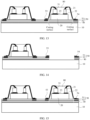
- Step 001 Provide a substrate.
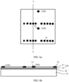
- FIG. 9a is a top view of a component
- FIG. 9b is a sectional view of a line A-A in FIG. 9a
- the drive chip 20 is assembled onto the line layer 50 by using the transfer process and a die attach (die attach) process.
- the transfer process may use a laser transfer manner or a physical transfer manner according to a wafer manufacturing process.
- the drive chip 20 is fixed on a line through film or adhesive die attach (adhesive die attach), and the IO pad 22 and the P pad 23 of the drive chip 20 face upward (a placement direction of the substrate 10 in FIG. 9b is used as a reference direction).
- Step 003 Dispose a sub-pixel.
- FIG. 10a is a top view of a component
- FIG. 10b is a sectional view of a line A-A in FIG. 10a
- the sub-pixel 31 uses the vertical structure shown in FIG. 4 .
- the sub-pixel 31 is assembled on a surface of the drive chip 20 by using the transfer process and the bonding process.
- a P pole (positive pole) of the sub-pixel 31 is connected to the P pad 23 of the drive chip 20.
- Step 004 Prepare a packaging layer.
- FIG. 11a is a top view of a component
- FIG. 11b is a sectional view of a line A-A in FIG. 11a
- the sub-pixel 31 and the drive chip 20 are packaged by using a PLN (Planarization) printing process to form a second packaging layer 80, and a negative pole (N pole) of the sub-pixel 31 and the IO pad 22 of the drive chip 20 are exposed by using a photolithography process.
- PLN Planarization
- a material of the second packaging layer 80 is a transparent material, which may be specifically a COF (Chip On Flex, or, Chip On Film, usually referred to as chip on film) material, may be a transparent photoresist material, or may be another transparent epoxy resin material.
- COF Chip On Flex, or, Chip On Film, usually referred to as chip on film
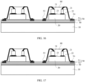
- Step 005 Perform fanout (fanout) and wiring.
- FIG. 12a is a top view of a component
- FIG. 12b is a sectional view of a line A-A in FIG. 12a
- Wiring of the IO pad 22 of the drive chip 20 is routed to a signal pad on a module surface (specifically, by disposing a binding post 21) by using the fanout process.
- a negative pole of each sub-pixel 31 is connected to the GND pad 54 of the line layer 50.
- a ground of the drive chip 20 is connected to a ground of the sub-pixel 31, and is connected to a ground of the display screen to connect all signal pins.
- Connection and wiring between the drive chip 20 and the line layer 50 may use a ⁇ bump (micro bump) process, which may be a Cu, an Al, or an ITO line process.
- ⁇ bump micro bump
- Step 006 Perform a test.
- a lighting test is performed on the stacked structure by using the DDIC. If there is a defective light-emitting unit, a position of the defective light-emitting unit is located.
- the defective light-emitting unit is cut by using a laser.
- the laser cuts the line layer 50 and the separation layer 40, so that the defective light-emitting unit is split.
- Step 008 Remove the defective light-emitting unit.
- a qualified light-emitting unit is transferred to a blank position by using a maintenance device, and is cured and fixed to the substrate 10 in a heating or UV (ultraviolet, ultraviolet) manner.
- Step 010 Fill in a gap around the repaired light-emitting unit.
- a position of a gap around the repaired light-emitting unit is filled up and cured by using a printing device.
- Step 011 Perform wiring to implement connection between the light-emitting unit and a line layer of the substrate.
- the drive chip and the pixel unit may be located at different layers, more drive chips may be arranged on the substrate, and more pixel units may also be arranged on the drive chips.
- the entire stacked structure may form an entire layer of pixel units, and the drive chips do not occupy an arrangement area of the pixel units, thereby increasing a quantity of the arranged pixel units, and further improving a display effect of the display screen.
- the light-emitting unit in the stacked structure may be replaced by using the separation layer during preparation, thereby improving reliability of the stacked structure during use.
- each drive chip 20 carries two rows of sub-pixels 31, but a vertical projection of each sub-pixel on the first surface is located in a vertical projection of the drive chip on the first surface.
- the first surface is a surface that is of the substrate and that faces the line layer.
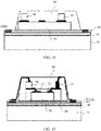
- FIG. 19 shows an example of another stacked structure according to an embodiment of this application.
- This stacked structure differs from the stacked structure shown in FIG. 3 in that a position for disposing the sub-pixel 31 is changed.
- the stacked structure shown in FIG. 19 includes a first packaging layer 90.
- Each drive chip 20 on the substrate 10 corresponds to one first packaging layer 90.
- Each first packaging layer 90 packages the corresponding drive chip 20, and a plurality of sub-pixels 31 corresponding to each drive chip 20 are disposed on the first packaging layer 90.
- vertical projections of the plurality of sub-pixels 31 on the first surface are located in a vertical projection of the drive chip 20 on the first surface.
- the first surface is the surface that is of the substrate 10 and that faces the line layer 50.
- the drive chip 20 may correspond to a plurality of pixel units 30, and the plurality of pixel units 30 are arranged in two rows, thereby increasing the quantity of the pixel units 30 corresponding to the drive chip 20.
- four pixel units 30 are distributed at four corners of a drive chip 20, and are connected to the drive chip 20 through wiring, to ensure that one drive chip 20 controls four pixel units 30. This can reduce the quantity of the disposed drive chips 20, increase the quantity of the pixel units 30 in the display screen, and improve a display effect of the display screen.
- connection ports 24, 25, and 26 are disposed in each drive chip 20.
- a middle row of connection ports 25 is connected to a binding post, and two rows of connection ports 24 and 26 on two sides are separately connected to the sub-pixels 31 in the pixel units 30.
- the middle binding post is connected to the IO pad 54 of the line layer 50
- each sub-pixel 31 is connected to the GND pad 53 of the line layer 50.
- the sub-pixels 31 of each drive chip 20 are connected in parallel, and then are connected to the line layer 50.
- FIG. 20 shows only a specific example, and another connection manner may be alternatively used.
- the sub-pixels 31 of each drive chip 20 are separately connected to the line layer 50.
- a process of preparing the first packaging layer 90 is added.
- the drive chip 20 may be packaged by using the PLN printing process, and an IO pad and a P pad of the drive chip 20 are exposed by using the photolithography process.
- the PLN material may be a transparent material or may be a non-transparent material.
- a material of the first packaging layer 90 may be a same material as that of the second packaging layer, for example, a COF material, or may be a transparent photoresist material or another transparent epoxy resin material.
- the sub-pixels 31 are prepared, the sub-pixels 31 are prepared on the first packaging layer 90, and the sub-pixels 31 are connected to the drive chip 20 through wiring.
- the vertical sub-pixel reduces a component area. Therefore, under a same ppi and brightness, a sub-pixel occupies a smaller area. Using this characteristic may maximize a ppi limit. When the ppi limit is not reached, transparent display may be implemented or another miniature component may be integrated.
- An embodiment of this application further provides a display screen.
- the display screen includes a housing and the stacked structure that is disposed inside the housing and that is described in any one of the foregoing solutions. It can be learned from the foregoing description that, when the pixel unit and the drive chip are stacked, the drive chip and the pixel unit may be located at different layers, more drive chips may be arranged on the substrate, and more pixel units may also be arranged on the drive chips.
- the entire stacked structure may form an entire layer of pixel units, and the drive chips do not occupy an arrangement area of the pixel units, thereby increasing a quantity of the arranged pixel units, and further improving a display effect of the display screen.
Landscapes
- Engineering & Computer Science (AREA)
- Physics & Mathematics (AREA)
- Computer Hardware Design (AREA)
- General Physics & Mathematics (AREA)
- Theoretical Computer Science (AREA)
- Devices For Indicating Variable Information By Combining Individual Elements (AREA)
- Led Device Packages (AREA)
- Electroluminescent Light Sources (AREA)
Applications Claiming Priority (2)
| Application Number | Priority Date | Filing Date | Title |
|---|---|---|---|
| CN202010362184.1A CN113594194B (zh) | 2020-04-30 | 2020-04-30 | 一种堆叠结构、显示屏及显示装置 |
| PCT/CN2021/090892 WO2021219069A1 (fr) | 2020-04-30 | 2021-04-29 | Structure empilée, écran d'affichage et dispositif d'affichage |
Publications (2)
| Publication Number | Publication Date |
|---|---|
| EP4131385A1 true EP4131385A1 (fr) | 2023-02-08 |
| EP4131385A4 EP4131385A4 (fr) | 2023-12-06 |
Family
ID=78237135
Family Applications (1)
| Application Number | Title | Priority Date | Filing Date |
|---|---|---|---|
| EP21797561.4A Pending EP4131385A4 (fr) | 2020-04-30 | 2021-04-29 | Structure empilée, écran d'affichage et dispositif d'affichage |
Country Status (6)
| Country | Link |
|---|---|
| US (1) | US12020630B1 (fr) |
| EP (1) | EP4131385A4 (fr) |
| JP (1) | JP7477647B2 (fr) |
| KR (1) | KR102759599B1 (fr) |
| CN (1) | CN113594194B (fr) |
| WO (1) | WO2021219069A1 (fr) |
Families Citing this family (5)
| Publication number | Priority date | Publication date | Assignee | Title |
|---|---|---|---|---|
| CN114974083A (zh) * | 2022-05-09 | 2022-08-30 | 武汉华星光电半导体显示技术有限公司 | 显示装置 |
| CN115206952B (zh) * | 2022-07-27 | 2023-03-17 | 北京数字光芯集成电路设计有限公司 | 采用堆叠式封装的Micro-LED微显示芯片 |
| CN116469971B (zh) * | 2023-04-18 | 2023-09-15 | 上海聚跃检测技术有限公司 | 一种集成电路堆叠芯片的封装方法及装置 |
| CN116995072B (zh) * | 2023-09-27 | 2023-12-08 | 惠科股份有限公司 | 显示背板及其制作方法和转移方法 |
| CN118213363B (zh) * | 2024-05-22 | 2024-08-27 | 华引芯(武汉)科技有限公司 | 发光器件、灯板和显示装置 |
Family Cites Families (29)
| Publication number | Priority date | Publication date | Assignee | Title |
|---|---|---|---|---|
| JP4951018B2 (ja) * | 2009-03-30 | 2012-06-13 | 株式会社東芝 | 半導体装置の製造方法 |
| KR101711961B1 (ko) * | 2010-09-10 | 2017-03-03 | 삼성전자주식회사 | 발광 디바이스 |
| CN201910207U (zh) * | 2010-11-22 | 2011-07-27 | 金建电子有限公司 | 一种高密度全彩led显示板 |
| JP5966412B2 (ja) * | 2011-04-08 | 2016-08-10 | ソニー株式会社 | 画素チップ、表示パネル、照明パネル、表示装置および照明装置 |
| ES2692524T3 (es) * | 2011-07-26 | 2018-12-04 | Gogoro Inc. | Aparato, método y artículo para proporcionar datos de diagnóstico de vehículo |
| US9159700B2 (en) | 2012-12-10 | 2015-10-13 | LuxVue Technology Corporation | Active matrix emissive micro LED display |
| CN103545304A (zh) * | 2013-11-01 | 2014-01-29 | 广东威创视讯科技股份有限公司 | 一种发光二极管和驱动芯片的封装结构及封装方法 |
| US9367094B2 (en) * | 2013-12-17 | 2016-06-14 | Apple Inc. | Display module and system applications |
| TWI814461B (zh) | 2014-06-18 | 2023-09-01 | 愛爾蘭商艾克斯展示公司技術有限公司 | 微組裝發光二極體顯示器及照明元件 |
| GB201418810D0 (en) * | 2014-10-22 | 2014-12-03 | Infiniled Ltd | Display |
| WO2017020300A1 (fr) * | 2015-08-06 | 2017-02-09 | 林谊 | Point de pixel del, composant électroluminescent, panneau électroluminescent et écran d'affichage |
| CN205016161U (zh) * | 2015-08-06 | 2016-02-03 | 林谊 | Led像素点、发光组件、发光面板和显示屏 |
| US10665578B2 (en) * | 2015-09-24 | 2020-05-26 | Apple Inc. | Display with embedded pixel driver chips |
| EP3384530A1 (fr) * | 2016-02-18 | 2018-10-10 | Apple Inc. | Structure de fond de panier et procédé pour un microcircuit de commande et micro-del |
| TWI646680B (zh) * | 2017-01-10 | 2019-01-01 | 英屬開曼群島商錼創科技股份有限公司 | 微型發光二極體晶片以及顯示面板 |
| US12015103B2 (en) * | 2017-01-10 | 2024-06-18 | PlayNitride Display Co., Ltd. | Micro light emitting diode display panel with option of choosing to emit light both or respectively of light-emitting regions |
| CN106816502B (zh) * | 2017-04-12 | 2019-04-02 | 京东方科技集团股份有限公司 | 一种led芯片、led发光基板、显示装置及彩色显示控制方法 |
| US10319266B1 (en) * | 2017-04-24 | 2019-06-11 | Facebook Technologies, Llc | Display panel with non-visible light detection |
| KR102078643B1 (ko) * | 2018-04-04 | 2020-04-07 | (주)라이타이저 | 원칩 타입의 발광 다이오드를 이용한 디스플레이 장치 및 그 제조 방법 |
| CN110391261B (zh) * | 2018-04-18 | 2022-03-15 | 英属开曼群岛商镎创科技股份有限公司 | 微型发光二极管显示面板 |
| CN108987382A (zh) * | 2018-07-27 | 2018-12-11 | 京东方科技集团股份有限公司 | 一种电致发光器件及其制作方法 |
| TWI676851B (zh) * | 2018-08-22 | 2019-11-11 | 隆達電子股份有限公司 | 畫素陣列封裝結構及顯示面板 |
| CN109360838B (zh) * | 2018-09-26 | 2022-04-26 | 京东方科技集团股份有限公司 | 一种感控显示面板及感控显示装置 |
| CN109768027B (zh) * | 2019-01-29 | 2020-07-07 | 福州大学 | 一种Micro-LED显示屏的结构和制造方法 |
| CN110277059B (zh) * | 2019-07-01 | 2021-04-23 | 武汉天马微电子有限公司 | 驱动芯片及其控制方法、显示装置 |
| CN210167355U (zh) * | 2019-07-10 | 2020-03-20 | 深圳市兆驰节能照明股份有限公司 | 透明显示屏及其led光源 |
| CN110416171A (zh) * | 2019-09-05 | 2019-11-05 | 东莞市欧思科光电科技有限公司 | 一体化光电显示单元及其制作工艺、光电显示装置 |
| CN110600463A (zh) * | 2019-10-09 | 2019-12-20 | 深圳韦侨顺光电有限公司 | 基于芯片堆叠的集成封装led显示面板 |
| CN112700749B (zh) * | 2021-01-04 | 2022-04-26 | 武汉天马微电子有限公司 | 显示面板的驱动方法及其驱动装置、显示装置 |
-
2020
- 2020-04-30 CN CN202010362184.1A patent/CN113594194B/zh active Active
-
2021
- 2021-04-29 WO PCT/CN2021/090892 patent/WO2021219069A1/fr not_active Ceased
- 2021-04-29 KR KR1020227041264A patent/KR102759599B1/ko active Active
- 2021-04-29 JP JP2022565957A patent/JP7477647B2/ja active Active
- 2021-04-29 EP EP21797561.4A patent/EP4131385A4/fr active Pending
-
2022
- 2022-10-28 US US17/975,696 patent/US12020630B1/en active Active
Also Published As
| Publication number | Publication date |
|---|---|
| JP7477647B2 (ja) | 2024-05-01 |
| US12020630B1 (en) | 2024-06-25 |
| EP4131385A4 (fr) | 2023-12-06 |
| WO2021219069A1 (fr) | 2021-11-04 |
| JP2023523758A (ja) | 2023-06-07 |
| CN113594194A (zh) | 2021-11-02 |
| CN113594194B (zh) | 2024-09-17 |
| KR102759599B1 (ko) | 2025-01-23 |
| KR20230006528A (ko) | 2023-01-10 |
Similar Documents
| Publication | Publication Date | Title |
|---|---|---|
| JP7473702B2 (ja) | シリコン上のカラーiledディスプレイ | |
| US12020630B1 (en) | Stacked structure, display screen, and display apparatus | |
| US10790267B2 (en) | Light emitting element for pixel and LED display module | |
| CN111933630B (zh) | Led芯片封装模块、显示屏及其制作方法 | |
| CN111048656B (zh) | 显示装置及该显示装置的制造方法 | |
| EP3128505B1 (fr) | Substrat de montage et dispositif électronique | |
| JP6128046B2 (ja) | 実装基板および電子機器 | |
| TW202115862A (zh) | 具有控制器和光發射器的像素模組 | |
| CN213519057U (zh) | 显示装置 | |
| US11296061B2 (en) | Micro semiconductor stacked structure and electronic apparatus having the same | |
| KR102519201B1 (ko) | 픽셀용 발광소자 및 엘이디 디스플레이 장치 | |
| KR20180093767A (ko) | 반도체 발광 소자를 이용한 디스플레이 장치 | |
| JP2017139489A (ja) | 表示装置 | |
| CN118173686A (zh) | 一种像素单元及制备方法、显示面板 | |
| CN116454077A (zh) | 用于显示屏的发光模块 | |
| KR102759226B1 (ko) | 마이크로 led 패키지 및 이를 구비한 디스플레이 | |
| CN113903760B (zh) | 一种堆叠结构、显示屏及显示装置 | |
| US20250364503A1 (en) | Manufacturing method of micro light-emitting diode display device | |
| US20260082754A1 (en) | Multilayer board structure and display device | |
| CN115911218A (zh) | 微型发光二极管显示设备与其制造方法 | |
| CN118173694A (zh) | 发光芯片及其制备方法、发光基板及显示装置 |
Legal Events
| Date | Code | Title | Description |
|---|---|---|---|
| STAA | Information on the status of an ep patent application or granted ep patent |
Free format text: STATUS: THE INTERNATIONAL PUBLICATION HAS BEEN MADE |
|
| PUAI | Public reference made under article 153(3) epc to a published international application that has entered the european phase |
Free format text: ORIGINAL CODE: 0009012 |
|
| STAA | Information on the status of an ep patent application or granted ep patent |
Free format text: STATUS: REQUEST FOR EXAMINATION WAS MADE |
|
| 17P | Request for examination filed |
Effective date: 20221104 |
|
| AK | Designated contracting states |
Kind code of ref document: A1 Designated state(s): AL AT BE BG CH CY CZ DE DK EE ES FI FR GB GR HR HU IE IS IT LI LT LU LV MC MK MT NL NO PL PT RO RS SE SI SK SM TR |
|
| DAV | Request for validation of the european patent (deleted) | ||
| DAX | Request for extension of the european patent (deleted) | ||
| A4 | Supplementary search report drawn up and despatched |
Effective date: 20231108 |
|
| RIC1 | Information provided on ipc code assigned before grant |
Ipc: H01L 33/62 20100101ALN20231102BHEP Ipc: H01L 25/16 20230101ALI20231102BHEP Ipc: H01L 25/075 20060101ALI20231102BHEP Ipc: H01L 27/15 20060101AFI20231102BHEP |