EP4135007A1 - Verfahren zur herstellung von hochfrequenzkomponenten - Google Patents
Verfahren zur herstellung von hochfrequenzkomponenten Download PDFInfo
- Publication number
- EP4135007A1 EP4135007A1 EP22188356.4A EP22188356A EP4135007A1 EP 4135007 A1 EP4135007 A1 EP 4135007A1 EP 22188356 A EP22188356 A EP 22188356A EP 4135007 A1 EP4135007 A1 EP 4135007A1
- Authority
- EP
- European Patent Office
- Prior art keywords
- substrate
- layer
- laser
- components
- upper face
- Prior art date
- Legal status (The legal status is an assumption and is not a legal conclusion. Google has not performed a legal analysis and makes no representation as to the accuracy of the status listed.)
- Pending
Links
Images
Classifications
-
- H—ELECTRICITY
- H10—SEMICONDUCTOR DEVICES; ELECTRIC SOLID-STATE DEVICES NOT OTHERWISE PROVIDED FOR
- H10P—GENERIC PROCESSES OR APPARATUS FOR THE MANUFACTURE OR TREATMENT OF DEVICES COVERED BY CLASS H10
- H10P90/00—Preparation of wafers not covered by a single main group of this subclass, e.g. wafer reinforcement
-
- H—ELECTRICITY
- H10—SEMICONDUCTOR DEVICES; ELECTRIC SOLID-STATE DEVICES NOT OTHERWISE PROVIDED FOR
- H10P—GENERIC PROCESSES OR APPARATUS FOR THE MANUFACTURE OR TREATMENT OF DEVICES COVERED BY CLASS H10
- H10P95/00—Generic processes or apparatus for manufacture or treatments not covered by the other groups of this subclass
- H10P95/90—Thermal treatments, e.g. annealing or sintering
- H10P95/906—Thermal treatments, e.g. annealing or sintering for altering the shape of semiconductors, e.g. smoothing the surface
-
- H—ELECTRICITY
- H10—SEMICONDUCTOR DEVICES; ELECTRIC SOLID-STATE DEVICES NOT OTHERWISE PROVIDED FOR
- H10P—GENERIC PROCESSES OR APPARATUS FOR THE MANUFACTURE OR TREATMENT OF DEVICES COVERED BY CLASS H10
- H10P14/00—Formation of materials, e.g. in the shape of layers or pillars
- H10P14/20—Formation of materials, e.g. in the shape of layers or pillars of semiconductor materials
- H10P14/26—Formation of materials, e.g. in the shape of layers or pillars of semiconductor materials using liquid deposition
- H10P14/263—Formation of materials, e.g. in the shape of layers or pillars of semiconductor materials using liquid deposition using melted materials
-
- H—ELECTRICITY
- H10—SEMICONDUCTOR DEVICES; ELECTRIC SOLID-STATE DEVICES NOT OTHERWISE PROVIDED FOR
- H10P—GENERIC PROCESSES OR APPARATUS FOR THE MANUFACTURE OR TREATMENT OF DEVICES COVERED BY CLASS H10
- H10P14/00—Formation of materials, e.g. in the shape of layers or pillars
- H10P14/60—Formation of materials, e.g. in the shape of layers or pillars of insulating materials
- H10P14/65—Formation of materials, e.g. in the shape of layers or pillars of insulating materials characterised by treatments performed before or after the formation of the materials
- H10P14/6502—Formation of materials, e.g. in the shape of layers or pillars of insulating materials characterised by treatments performed before or after the formation of the materials of treatments performed before formation of the materials
- H10P14/6509—Formation of materials, e.g. in the shape of layers or pillars of insulating materials characterised by treatments performed before or after the formation of the materials of treatments performed before formation of the materials by exposure to electromagnetic radiation, e.g. UV light
-
- H—ELECTRICITY
- H10—SEMICONDUCTOR DEVICES; ELECTRIC SOLID-STATE DEVICES NOT OTHERWISE PROVIDED FOR
- H10P—GENERIC PROCESSES OR APPARATUS FOR THE MANUFACTURE OR TREATMENT OF DEVICES COVERED BY CLASS H10
- H10P14/00—Formation of materials, e.g. in the shape of layers or pillars
- H10P14/60—Formation of materials, e.g. in the shape of layers or pillars of insulating materials
- H10P14/65—Formation of materials, e.g. in the shape of layers or pillars of insulating materials characterised by treatments performed before or after the formation of the materials
- H10P14/6516—Formation of materials, e.g. in the shape of layers or pillars of insulating materials characterised by treatments performed before or after the formation of the materials of treatments performed after formation of the materials
- H10P14/6518—Formation of materials, e.g. in the shape of layers or pillars of insulating materials characterised by treatments performed before or after the formation of the materials of treatments performed after formation of the materials by introduction of substances into an already-existing insulating layer
- H10P14/6519—Formation of materials, e.g. in the shape of layers or pillars of insulating materials characterised by treatments performed before or after the formation of the materials of treatments performed after formation of the materials by introduction of substances into an already-existing insulating layer the substance being oxygen
-
- H—ELECTRICITY
- H10—SEMICONDUCTOR DEVICES; ELECTRIC SOLID-STATE DEVICES NOT OTHERWISE PROVIDED FOR
- H10P—GENERIC PROCESSES OR APPARATUS FOR THE MANUFACTURE OR TREATMENT OF DEVICES COVERED BY CLASS H10
- H10P34/00—Irradiation with electromagnetic or particle radiation of wafers, substrates or parts of devices
- H10P34/40—Irradiation with electromagnetic or particle radiation of wafers, substrates or parts of devices with high-energy radiation
- H10P34/42—Irradiation with electromagnetic or particle radiation of wafers, substrates or parts of devices with high-energy radiation with electromagnetic radiation, e.g. laser annealing
-
- H—ELECTRICITY
- H10—SEMICONDUCTOR DEVICES; ELECTRIC SOLID-STATE DEVICES NOT OTHERWISE PROVIDED FOR
- H10P—GENERIC PROCESSES OR APPARATUS FOR THE MANUFACTURE OR TREATMENT OF DEVICES COVERED BY CLASS H10
- H10P90/00—Preparation of wafers not covered by a single main group of this subclass, e.g. wafer reinforcement
- H10P90/19—Preparing inhomogeneous wafers
- H10P90/1904—Preparing vertically inhomogeneous wafers
- H10P90/1906—Preparing SOI wafers
-
- H—ELECTRICITY
- H10—SEMICONDUCTOR DEVICES; ELECTRIC SOLID-STATE DEVICES NOT OTHERWISE PROVIDED FOR
- H10P—GENERIC PROCESSES OR APPARATUS FOR THE MANUFACTURE OR TREATMENT OF DEVICES COVERED BY CLASS H10
- H10P95/00—Generic processes or apparatus for manufacture or treatments not covered by the other groups of this subclass
- H10P95/40—Treatments of semiconductor bodies to modify their internal properties, e.g. to produce internal imperfections
- H10P95/402—Treatments of semiconductor bodies to modify their internal properties, e.g. to produce internal imperfections of silicon bodies
-
- H—ELECTRICITY
- H10—SEMICONDUCTOR DEVICES; ELECTRIC SOLID-STATE DEVICES NOT OTHERWISE PROVIDED FOR
- H10W—GENERIC PACKAGES, INTERCONNECTIONS, CONNECTORS OR OTHER CONSTRUCTIONAL DETAILS OF DEVICES COVERED BY CLASS H10
- H10W10/00—Isolation regions in semiconductor bodies between components of integrated devices
- H10W10/10—Isolation regions comprising dielectric materials
- H10W10/181—Semiconductor-on-insulator [SOI] isolation regions, e.g. buried oxide regions of SOI wafers
Definitions
- This description relates to the field of electronic components in general. It is aimed more particularly at the field of radio frequency components.
- Radiofrequency components are generally called components whose operating frequency is in the range from 3 kHz to 30 GHz.
- Known radio frequency components include active components such as amplifiers, mixers, and data converters, and passive components such as capacitors, inductors, and antennas.
- the substrate has a resistivity greater than 3 k ⁇ .cm.
- the method comprises, before step a), a step of forming an oxide layer on the side of the upper face of the substrate.
- the power of the laser during step a) is of the order of 4j/cm 2 .
- the substrate is made of silicon or of gallium nitride.
- the laser has a wavelength comprised between 300 nm and 700 nm.
- step a the first thickness of the substrate is melted.
- step a) is followed by a substrate cooling step.
- the first thickness is between 0.5 ⁇ m and 2 ⁇ m, for example, of the order of 1 ⁇ m.
- said at least one radiofrequency component is a passive component made of a metallic material arranged on and in contact with the upper face of the insulating layer.
- FIG. 1 is a sectional view illustrating an example of a device comprising radiofrequency components 15.
- the device illustrated in figure 1 comprises a semiconductor substrate 11 coated with a passivation layer 13, on which the radio frequency components 15 are arranged.
- the passivation layer 13 is for example, in contact, by its lower face, with the upper face of the semiconductor substrate passivation 13 extends for example continuously over the entire surface of the semiconductor substrate 11.
- the device comprises two radiofrequency components 15.
- the device may comprise any number of radiofrequency components 15, for example a single radiofrequency component 15 or more than two radiofrequency components 15.
- the substrate 11 corresponds for example to a semiconductor wafer or to a piece of semiconductor wafer.
- the substrate 11 is for example made of silicon or of gallium nitride (GaN).
- the substrate 11 is made of a high resistivity material, for example a material whose resistivity is greater than 3 k ⁇ .cm.
- the substrate 11 is for example made of high resistivity silicon.
- the substrate 11 can be a solid semiconductor substrate, for example a solid high resistivity silicon substrate, or an SOI (Semiconductor On Insulator) type substrate, for example a silicon substrate of high resistivity on insulation.
- Passivation layer 13 is an electrically insulating layer.
- the passivation layer 13 is for example made of silicon dioxide.
- induced currents may appear in an upper part 17 of the substrate 11, called the parasitic surface conduction zone (PSC, standing for “Parasitic Surface Conduction”). These induced currents can disturb the correct operation of the radio frequency components 15 and degrade their performance.
- PSC parasitic surface conduction zone
- This technique usually used to activate or propagate dopants in a semiconductor layer, is in this embodiment used in an unusual way, to deliberately create defects in a semiconductor layer.
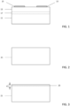
- THE figures 2 to 6 are cross-sectional views illustrating successive steps of an example of a method of manufacturing a device comprising radiofrequency components according to one embodiment.
- the substrate 21 is for example a wafer or wafer made of a semiconductor material.
- substrate 21 is made of silicon or gallium nitride.
- the substrate 21 is made of a high resistivity material.
- Substrate 21 can be a solid semiconductor substrate, or an SOI type substrate.
- the substrate 21 has for example a thickness comprised between 300 ⁇ m and 800 ⁇ m, for example of the order of 725 ⁇ m.
- the substrate 21 is not doped or is very lightly doped.
- the concentration of dopants in the substrate 21 is, for example, less than about 10 12 atoms/cm 3 for phosphorus atoms and, for example, less than about 4.10 12 atoms/cm 3 for boron atoms.
- the dopants present in the substrate 21 can be different from phosphorus and boron and can be arsenic or antimony.
- FIG. 3 illustrates the structure obtained at the end of a step of forming an insulating layer 23 on the side of the upper face of the substrate 21.
- layer 23 is an oxide layer.
- an upper part of substrate 21 is oxidized so as to form layer 23.
- Layer 23 then corresponds to an upper part of substrate 21.
- Layer 23 has the same chemical composition as substrate 21 except that it includes a higher concentration of oxygen atoms.
- layer 23 has a thickness e1 of between 5 nm and 30 nm, for example between 15 nm and 20 nm.
- layer 23 is formed by thermal or chemical oxidation of an upper part of substrate 21.
- layer 23 is formed during cleaning of the upper face of substrate 21 in a mixture of sulfuric acid and hydrogen peroxide.
- layer 23 is a native oxide layer present on the surface of substrate 21.
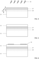
- FIG. 4 illustrates the structure obtained at the end of a laser annealing step from the upper face of the structure illustrated in picture 3 .
- the laser annealing step illustrated in relation to the picture 3 comprises two successive stages.
- the upper surface of the structure is exposed to radiation from a laser 25, for example a pulsed laser.
- a laser 25 for example a pulsed laser.
- the upper surface of the structure is exposed to radiation from the laser 25 until an upper part of the semiconductor material of the substrate 21 is melted.
- the reference 27 designates an upper layer of the structure of thickness e2 , melted under the effect of laser radiation.
- the thickness e2 depends in particular on the power of the laser 25, the wavelength of the laser 25, the material of the substrate 21, and, where appropriate, the duration and frequency of the pulses of the laser 25.
- the power of the laser 25 is of the order of 4 J/cm 2 .
- the wavelength of the laser 25 can be chosen according to the material of the substrate 21.
- the wavelength of the laser 25 can be less than 500 nm, and, for a substrate 21 made of gallium nitride, the wavelength of the laser 25 can be less at 400nm.
- the thickness e2 is for example between 0.5 ⁇ m and 2 ⁇ m, for example of the order of 1 ⁇ m.
- the structure and more particularly the upper layer 27 of the structure is cooled, preferably rapidly.
- the cooling rate is preferably greater than the cooling rate. Crystallization of the material of the substrate 21 so that the layer 27 does not recrystallize and remains in an amorphous state.
- the substrate 21 has, in its upper part 27, defects resulting from the incorporation of oxygen atoms (coming in particular from the oxide layer 23 and from the annealing chamber atmosphere) and carbon (from the annealing chamber atmosphere) in the substrate material.
- the defects formed in layer 27 are in the form of complexes between carbon atoms and silicon atoms and of complexes between carbon atoms and silicon atoms. of oxygen. These defects are suitable for trapping any charge carriers present in layer 27.
- the density of defects generated in the upper part 27 of the substrate 21 during the annealing step depends in particular on the heating rate and the cooling rate of the substrate 21. In particular, the higher the heating rate, the faster is the cooling, the greater the defect density.
- another layer 29 of substrate 21, located under and in contact with molten layer 27, also undergoes transformations.
- crystalline structure defects of the structure tend to propagate in the thickness of the substrate 21 under the layer 27.
- the layer 29 of the substrate 21 does not melt and remains crystalline.
- Layer 29 extends into substrate 21 from the underside of part 27 over a thickness e3.
- the thickness e3 is between 0.5 ⁇ m and 2 ⁇ m, for example of the order of 1 ⁇ m.
- Layer 29 contains defects of the void type ("voids" or "gaps" in English), adapted to trap any charge carriers present in the layer 29.
- the laser annealing step mentioned above is carried out full plate, that is to say that it is carried out over the entire surface of the substrate 21.
- the laser annealing step mentioned above is carried out locally on the surface of the substrate 21.
- the precision or resolution of the laser is, for example, of the order of a few micrometers.
- the laser annealing step does not cause texturing of the surface of the substrate 21.
- the upper face of the substrate 21, and more particularly the upper face of the layer 27 is flat at the end of the step of laser annealing.
- FIG 5 illustrates the structure obtained at the end of a step of depositing an electrically insulating layer or passivation layer 31 on the surface of the structure illustrated in figure 4 .
- layer 31 is made of an oxide, for example silicon dioxide.
- layer 31 is deposited full plate on the surface of the device illustrated in figure 4 , that is to say that it is deposited so as to completely cover the upper face of the substrate 21.
- the layer 31 has a thickness of between 0.5 ⁇ m and 2 ⁇ m, for example of the order of 1.2 ⁇ m.
- FIG. 6 illustrates the device obtained at the end of a step of forming radio frequency components 33 on the insulating layer 31.
- the device comprises two radiofrequency components 33.
- the device can carry any number of components radio frequency 33, for example, a single radio frequency component 33 or more than two radio frequency components 33.
- the radio frequency components 33 are passive components, for example inductors or antennas.
- the radiofrequency components 33 are for example made of a metallic material, for example copper or aluminum.
- the radiofrequency components 33 are configured to operate in a frequency range comprised between a few kilohertz and a few gigahertz, for example between 3 kHz and 30 GHz.
- An advantage of the method described in relation to the figures 2 to 6 is that it makes it possible, by means of a laser annealing technique that is relatively simple to implement, to produce a surface layer rich in traps in a semiconductor substrate intended to support radio frequency components.
- the proposed method makes it possible, at low cost, to obtain a high density of traps, and thus to significantly reduce the parasitic currents induced in the substrate and therefore to improve the performance of the radiofrequency components.
Landscapes
- Formation Of Insulating Films (AREA)
- Physics & Mathematics (AREA)
- Electromagnetism (AREA)
- Semiconductor Integrated Circuits (AREA)
- Element Separation (AREA)
Applications Claiming Priority (1)
| Application Number | Priority Date | Filing Date | Title |
|---|---|---|---|
| FR2108655A FR3126169B1 (fr) | 2021-08-12 | 2021-08-12 | Procédé de fabrication de composants radiofréquence |
Publications (1)
| Publication Number | Publication Date |
|---|---|
| EP4135007A1 true EP4135007A1 (de) | 2023-02-15 |
Family
ID=77913274
Family Applications (1)
| Application Number | Title | Priority Date | Filing Date |
|---|---|---|---|
| EP22188356.4A Pending EP4135007A1 (de) | 2021-08-12 | 2022-08-02 | Verfahren zur herstellung von hochfrequenzkomponenten |
Country Status (4)
| Country | Link |
|---|---|
| US (2) | US12261059B2 (de) |
| EP (1) | EP4135007A1 (de) |
| CN (2) | CN219123214U (de) |
| FR (1) | FR3126169B1 (de) |
Families Citing this family (1)
| Publication number | Priority date | Publication date | Assignee | Title |
|---|---|---|---|---|
| FR3126169B1 (fr) * | 2021-08-12 | 2024-08-30 | St Microelectronics Tours Sas | Procédé de fabrication de composants radiofréquence |
Citations (5)
| Publication number | Priority date | Publication date | Assignee | Title |
|---|---|---|---|---|
| US20030218171A1 (en) * | 2002-01-28 | 2003-11-27 | Atsuo Isobe | Semiconductor device and method of manufacturing the same |
| US20190057868A1 (en) * | 2017-05-19 | 2019-02-21 | Psemi Corporation | Managed Substrate Effects for Stabilized SOI FETs |
| US20200161336A1 (en) * | 2017-06-13 | 2020-05-21 | Commissariat A L'energie Atomique Et Aux Energies Alternatives | Soi substrate compatible with the rfsoi and fdsoi technologies |
| US20210183690A1 (en) * | 2019-12-17 | 2021-06-17 | Commissariat A L'energie Atomique Et Aux Energies Alternatives | Manufacturing process of an rf-soi trapping layer substrate resulting from a crystalline transformation of a buried layer |
| US11081407B2 (en) * | 2017-02-10 | 2021-08-03 | Globalwafers Co., Ltd. | Methods for assessing semiconductor structures |
Family Cites Families (11)
| Publication number | Priority date | Publication date | Assignee | Title |
|---|---|---|---|---|
| US8304324B2 (en) * | 2008-05-16 | 2012-11-06 | Corporation For National Research Initiatives | Low-temperature wafer bonding of semiconductors to metals |
| US8236706B2 (en) * | 2008-12-12 | 2012-08-07 | Mattson Technology, Inc. | Method and apparatus for growing thin oxide films on silicon while minimizing impact on existing structures |
| US8536021B2 (en) * | 2010-12-24 | 2013-09-17 | Io Semiconductor, Inc. | Trap rich layer formation techniques for semiconductor devices |
| US11088050B2 (en) * | 2012-04-09 | 2021-08-10 | Monolithic 3D Inc. | 3D semiconductor device with isolation layers |
| US10600888B2 (en) * | 2012-04-09 | 2020-03-24 | Monolithic 3D Inc. | 3D semiconductor device |
| FI130149B (en) * | 2013-11-26 | 2023-03-15 | Okmetic Oyj | High-resistive silicon substrate with a reduced radio frequency loss for a radio-frequency integrated passive device |
| JP6604300B2 (ja) * | 2016-10-14 | 2019-11-13 | 株式会社Sumco | シリコン接合ウェーハの製造方法 |
| FR3058561B1 (fr) * | 2016-11-04 | 2018-11-02 | Soitec | Procede de fabrication d'un element semi-conducteur comprenant un substrat hautement resistif |
| CN110085550A (zh) * | 2018-01-26 | 2019-08-02 | 沈阳硅基科技有限公司 | 一种半导体产品用绝缘层结构及其制备方法 |
| WO2021213410A1 (zh) * | 2020-04-21 | 2021-10-28 | 济南晶正电子科技有限公司 | 一种复合基板及其制备方法 |
| FR3126169B1 (fr) * | 2021-08-12 | 2024-08-30 | St Microelectronics Tours Sas | Procédé de fabrication de composants radiofréquence |
-
2021
- 2021-08-12 FR FR2108655A patent/FR3126169B1/fr active Active
-
2022
- 2022-08-02 EP EP22188356.4A patent/EP4135007A1/de active Pending
- 2022-08-03 US US17/880,473 patent/US12261059B2/en active Active
- 2022-08-11 CN CN202222112771.2U patent/CN219123214U/zh active Active
- 2022-08-11 CN CN202210966830.4A patent/CN115881648A/zh active Pending
-
2025
- 2025-02-14 US US19/054,558 patent/US20250191935A1/en active Pending
Patent Citations (5)
| Publication number | Priority date | Publication date | Assignee | Title |
|---|---|---|---|---|
| US20030218171A1 (en) * | 2002-01-28 | 2003-11-27 | Atsuo Isobe | Semiconductor device and method of manufacturing the same |
| US11081407B2 (en) * | 2017-02-10 | 2021-08-03 | Globalwafers Co., Ltd. | Methods for assessing semiconductor structures |
| US20190057868A1 (en) * | 2017-05-19 | 2019-02-21 | Psemi Corporation | Managed Substrate Effects for Stabilized SOI FETs |
| US20200161336A1 (en) * | 2017-06-13 | 2020-05-21 | Commissariat A L'energie Atomique Et Aux Energies Alternatives | Soi substrate compatible with the rfsoi and fdsoi technologies |
| US20210183690A1 (en) * | 2019-12-17 | 2021-06-17 | Commissariat A L'energie Atomique Et Aux Energies Alternatives | Manufacturing process of an rf-soi trapping layer substrate resulting from a crystalline transformation of a buried layer |
Also Published As
| Publication number | Publication date |
|---|---|
| FR3126169B1 (fr) | 2024-08-30 |
| CN115881648A (zh) | 2023-03-31 |
| US12261059B2 (en) | 2025-03-25 |
| CN219123214U (zh) | 2023-06-02 |
| US20250191935A1 (en) | 2025-06-12 |
| US20230048614A1 (en) | 2023-02-16 |
| FR3126169A1 (fr) | 2023-02-17 |
Similar Documents
| Publication | Publication Date | Title |
|---|---|---|
| EP1338030B1 (de) | Verfahren zur herstellung eines substrats inbesondere für optik,elektronik oder optoelektronik und danach hergestelltes substrat | |
| EP0351001B1 (de) | Verfahren zur Herstellung einer Halbleitervorrichtung mit mindestens einer kleine Kontaktlöcher enthaltenden Leiterbahn | |
| WO2006000691A1 (fr) | Support d'epitaxie hybride et son procede de fabrication | |
| EP3127142B1 (de) | Verfahren zur herstellung eines halbleiterwafers zur herstellung eines soi-substrats und damit hergestellter soi-substratwafer | |
| EP1292975A1 (de) | Verfahren zur herstellung von substraten und dadurch hergestellte substrate | |
| FR2794897A1 (fr) | Plaquette a semi-conducteur et dispositif a semi-conducteur fabrique a partir d'une telle plaquette | |
| EP4135007A1 (de) | Verfahren zur herstellung von hochfrequenzkomponenten | |
| EP0432044A1 (de) | III-V-Verbindungsleistungstransistor auf Siliciumsubstrat und Verfahren zur Herstellung | |
| EP1483793A2 (de) | Leistungs-schottkydiode mit sicoi-substrat und diesbezügliches herstellungsverfahren | |
| EP2337076A1 (de) | Mikroelektronischvorrichtung, insbesonde von hinten beleuchtete Abbildungsvorrichtung und Verfahren zur deren Herstellung | |
| FR2797999A1 (fr) | Procede de fabrication d'une capacite integree sur un substrat de silicium | |
| FR2538616A1 (fr) | Procede de fabrication collective de diodes hyperfrequence avec encapsulation incorporee et diodes ainsi obtenues | |
| EP1186024B1 (de) | Herstellungsverfahren für ein siliziumsubstrat mit einer dünnen, vergrabenen siliziumoxidschicht | |
| EP0085607A2 (de) | Verfahren zur gleichzeitigen Produktion von Hyperfrequenzdioden mit eingebauter Einkapselung und nach diesem Verfahren hergestellte Dioden | |
| EP4012735B1 (de) | Verfahren zur herstellung eines kondensators | |
| EP3853882A1 (de) | Verfahren zur herstellung einer elektronischen vorrichtung | |
| FR2536211A1 (fr) | Structure de diode hyperfrequences dont les connexions exterieures sont prises par deux poutres metalliques | |
| WO2018007711A1 (fr) | Dispositif cascode integre monolithiquement | |
| FR2724068A1 (fr) | Dispositif laser a semi-conducteur et procede de fabrication du dispositif laser a semi-conducteur | |
| FR3098014A1 (fr) | Composé intermétallique | |
| EP3859769B1 (de) | Verfahren zum ätzen im nanometerbereich einer germanium-zinn-legierung (gesn) für fet-transistor | |
| FR3094562A1 (fr) | Co-intégration de contacts sur des semiconducteurs différents | |
| EP1010202B1 (de) | Verfahren zur minimierung des randeffekts durch verdichten der isolationsschicht | |
| EP4362067A1 (de) | Verfahren zur herstellung eines elektronischen leistungsbauelements und bauelement erhalten durch dieses verfahren | |
| WO2024126599A1 (fr) | Procédé de préparation d'un empilement en vue d'un collage |
Legal Events
| Date | Code | Title | Description |
|---|---|---|---|
| PUAI | Public reference made under article 153(3) epc to a published international application that has entered the european phase |
Free format text: ORIGINAL CODE: 0009012 |
|
| STAA | Information on the status of an ep patent application or granted ep patent |
Free format text: STATUS: REQUEST FOR EXAMINATION WAS MADE |
|
| 17P | Request for examination filed |
Effective date: 20220802 |
|
| AK | Designated contracting states |
Kind code of ref document: A1 Designated state(s): AL AT BE BG CH CY CZ DE DK EE ES FI FR GB GR HR HU IE IS IT LI LT LU LV MC MK MT NL NO PL PT RO RS SE SI SK SM TR |
|
| REG | Reference to a national code |
Ref country code: DE Ref legal event code: R079 Free format text: PREVIOUS MAIN CLASS: H01L0021020000 Ipc: H10P0095000000 |
|
| GRAP | Despatch of communication of intention to grant a patent |
Free format text: ORIGINAL CODE: EPIDOSNIGR1 |
|
| STAA | Information on the status of an ep patent application or granted ep patent |
Free format text: STATUS: GRANT OF PATENT IS INTENDED |
|
| RIC1 | Information provided on ipc code assigned before grant |
Ipc: H10P 95/00 20260101AFI20260210BHEP Ipc: H10W 10/00 20260101ALI20260210BHEP |
|
| INTG | Intention to grant announced |
Effective date: 20260316 |