EP4135032A1 - Halbleitergehäuse mit reduzierter verbindungslänge - Google Patents
Halbleitergehäuse mit reduzierter verbindungslänge Download PDFInfo
- Publication number
- EP4135032A1 EP4135032A1 EP22187769.9A EP22187769A EP4135032A1 EP 4135032 A1 EP4135032 A1 EP 4135032A1 EP 22187769 A EP22187769 A EP 22187769A EP 4135032 A1 EP4135032 A1 EP 4135032A1
- Authority
- EP
- European Patent Office
- Prior art keywords
- package
- semiconductor package
- die
- tmvs
- vias
- Prior art date
- Legal status (The legal status is an assumption and is not a legal conclusion. Google has not performed a legal analysis and makes no representation as to the accuracy of the status listed.)
- Pending
Links
Images




Classifications
-
- H—ELECTRICITY
- H10—SEMICONDUCTOR DEVICES; ELECTRIC SOLID-STATE DEVICES NOT OTHERWISE PROVIDED FOR
- H10W—GENERIC PACKAGES, INTERCONNECTIONS, CONNECTORS OR OTHER CONSTRUCTIONAL DETAILS OF DEVICES COVERED BY CLASS H10
- H10W90/00—Package configurations
-
- H—ELECTRICITY
- H10—SEMICONDUCTOR DEVICES; ELECTRIC SOLID-STATE DEVICES NOT OTHERWISE PROVIDED FOR
- H10W—GENERIC PACKAGES, INTERCONNECTIONS, CONNECTORS OR OTHER CONSTRUCTIONAL DETAILS OF DEVICES COVERED BY CLASS H10
- H10W70/00—Package substrates; Interposers; Redistribution layers [RDL]
- H10W70/01—Manufacture or treatment
- H10W70/05—Manufacture or treatment of insulating or insulated package substrates, or of interposers, or of redistribution layers
- H10W70/08—Manufacture or treatment of insulating or insulated package substrates, or of interposers, or of redistribution layers by depositing layers on the chip or wafer, e.g. "chip-first" RDLs
- H10W70/09—Manufacture or treatment of insulating or insulated package substrates, or of interposers, or of redistribution layers by depositing layers on the chip or wafer, e.g. "chip-first" RDLs extending onto an encapsulation that laterally surrounds the chip or wafer, e.g. fan-out wafer level package [FOWLP] RDLs
-
- H—ELECTRICITY
- H10—SEMICONDUCTOR DEVICES; ELECTRIC SOLID-STATE DEVICES NOT OTHERWISE PROVIDED FOR
- H10W—GENERIC PACKAGES, INTERCONNECTIONS, CONNECTORS OR OTHER CONSTRUCTIONAL DETAILS OF DEVICES COVERED BY CLASS H10
- H10W70/00—Package substrates; Interposers; Redistribution layers [RDL]
- H10W70/60—Insulating or insulated package substrates; Interposers; Redistribution layers
-
- H—ELECTRICITY
- H10—SEMICONDUCTOR DEVICES; ELECTRIC SOLID-STATE DEVICES NOT OTHERWISE PROVIDED FOR
- H10W—GENERIC PACKAGES, INTERCONNECTIONS, CONNECTORS OR OTHER CONSTRUCTIONAL DETAILS OF DEVICES COVERED BY CLASS H10
- H10W70/00—Package substrates; Interposers; Redistribution layers [RDL]
- H10W70/60—Insulating or insulated package substrates; Interposers; Redistribution layers
- H10W70/611—Insulating or insulated package substrates; Interposers; Redistribution layers for connecting multiple chips together
-
- H—ELECTRICITY
- H10—SEMICONDUCTOR DEVICES; ELECTRIC SOLID-STATE DEVICES NOT OTHERWISE PROVIDED FOR
- H10W—GENERIC PACKAGES, INTERCONNECTIONS, CONNECTORS OR OTHER CONSTRUCTIONAL DETAILS OF DEVICES COVERED BY CLASS H10
- H10W70/00—Package substrates; Interposers; Redistribution layers [RDL]
- H10W70/60—Insulating or insulated package substrates; Interposers; Redistribution layers
- H10W70/611—Insulating or insulated package substrates; Interposers; Redistribution layers for connecting multiple chips together
- H10W70/614—Insulating or insulated package substrates; Interposers; Redistribution layers for connecting multiple chips together the multiple chips being integrally enclosed
-
- H—ELECTRICITY
- H10—SEMICONDUCTOR DEVICES; ELECTRIC SOLID-STATE DEVICES NOT OTHERWISE PROVIDED FOR
- H10W—GENERIC PACKAGES, INTERCONNECTIONS, CONNECTORS OR OTHER CONSTRUCTIONAL DETAILS OF DEVICES COVERED BY CLASS H10
- H10W70/00—Package substrates; Interposers; Redistribution layers [RDL]
- H10W70/60—Insulating or insulated package substrates; Interposers; Redistribution layers
- H10W70/62—Insulating or insulated package substrates; Interposers; Redistribution layers characterised by their interconnections
- H10W70/63—Vias, e.g. via plugs
- H10W70/635—Through-vias
-
- H—ELECTRICITY
- H10—SEMICONDUCTOR DEVICES; ELECTRIC SOLID-STATE DEVICES NOT OTHERWISE PROVIDED FOR
- H10W—GENERIC PACKAGES, INTERCONNECTIONS, CONNECTORS OR OTHER CONSTRUCTIONAL DETAILS OF DEVICES COVERED BY CLASS H10
- H10W70/00—Package substrates; Interposers; Redistribution layers [RDL]
- H10W70/60—Insulating or insulated package substrates; Interposers; Redistribution layers
- H10W70/62—Insulating or insulated package substrates; Interposers; Redistribution layers characterised by their interconnections
- H10W70/65—Shapes or dispositions of interconnections
-
- H—ELECTRICITY
- H10—SEMICONDUCTOR DEVICES; ELECTRIC SOLID-STATE DEVICES NOT OTHERWISE PROVIDED FOR
- H10W—GENERIC PACKAGES, INTERCONNECTIONS, CONNECTORS OR OTHER CONSTRUCTIONAL DETAILS OF DEVICES COVERED BY CLASS H10
- H10W70/00—Package substrates; Interposers; Redistribution layers [RDL]
- H10W70/60—Insulating or insulated package substrates; Interposers; Redistribution layers
- H10W70/67—Insulating or insulated package substrates; Interposers; Redistribution layers characterised by their insulating layers or insulating parts
- H10W70/68—Shapes or dispositions thereof
- H10W70/685—Shapes or dispositions thereof comprising multiple insulating layers
-
- H—ELECTRICITY
- H10—SEMICONDUCTOR DEVICES; ELECTRIC SOLID-STATE DEVICES NOT OTHERWISE PROVIDED FOR
- H10W—GENERIC PACKAGES, INTERCONNECTIONS, CONNECTORS OR OTHER CONSTRUCTIONAL DETAILS OF DEVICES COVERED BY CLASS H10
- H10W74/00—Encapsulations, e.g. protective coatings
- H10W74/10—Encapsulations, e.g. protective coatings characterised by their shape or disposition
- H10W74/111—Encapsulations, e.g. protective coatings characterised by their shape or disposition the semiconductor body being completely enclosed
- H10W74/114—Encapsulations, e.g. protective coatings characterised by their shape or disposition the semiconductor body being completely enclosed by a substrate and the encapsulations
- H10W74/117—Encapsulations, e.g. protective coatings characterised by their shape or disposition the semiconductor body being completely enclosed by a substrate and the encapsulations the substrate having spherical bumps for external connection
-
- H—ELECTRICITY
- H10—SEMICONDUCTOR DEVICES; ELECTRIC SOLID-STATE DEVICES NOT OTHERWISE PROVIDED FOR
- H10W—GENERIC PACKAGES, INTERCONNECTIONS, CONNECTORS OR OTHER CONSTRUCTIONAL DETAILS OF DEVICES COVERED BY CLASS H10
- H10W90/00—Package configurations
- H10W90/401—Package configurations characterised by multiple insulating or insulated package substrates, interposers or RDLs
-
- H—ELECTRICITY
- H10—SEMICONDUCTOR DEVICES; ELECTRIC SOLID-STATE DEVICES NOT OTHERWISE PROVIDED FOR
- H10W—GENERIC PACKAGES, INTERCONNECTIONS, CONNECTORS OR OTHER CONSTRUCTIONAL DETAILS OF DEVICES COVERED BY CLASS H10
- H10W90/00—Package configurations
- H10W90/701—Package configurations characterised by the relative positions of pads or connectors relative to package parts
-
- H—ELECTRICITY
- H10—SEMICONDUCTOR DEVICES; ELECTRIC SOLID-STATE DEVICES NOT OTHERWISE PROVIDED FOR
- H10W—GENERIC PACKAGES, INTERCONNECTIONS, CONNECTORS OR OTHER CONSTRUCTIONAL DETAILS OF DEVICES COVERED BY CLASS H10
- H10W70/00—Package substrates; Interposers; Redistribution layers [RDL]
- H10W70/099—Connecting interconnections to insulating or insulated package substrates, interposers or redistribution layers
-
- H—ELECTRICITY
- H10—SEMICONDUCTOR DEVICES; ELECTRIC SOLID-STATE DEVICES NOT OTHERWISE PROVIDED FOR
- H10W—GENERIC PACKAGES, INTERCONNECTIONS, CONNECTORS OR OTHER CONSTRUCTIONAL DETAILS OF DEVICES COVERED BY CLASS H10
- H10W70/00—Package substrates; Interposers; Redistribution layers [RDL]
- H10W70/60—Insulating or insulated package substrates; Interposers; Redistribution layers
- H10W70/62—Insulating or insulated package substrates; Interposers; Redistribution layers characterised by their interconnections
- H10W70/63—Vias, e.g. via plugs
-
- H—ELECTRICITY
- H10—SEMICONDUCTOR DEVICES; ELECTRIC SOLID-STATE DEVICES NOT OTHERWISE PROVIDED FOR
- H10W—GENERIC PACKAGES, INTERCONNECTIONS, CONNECTORS OR OTHER CONSTRUCTIONAL DETAILS OF DEVICES COVERED BY CLASS H10
- H10W70/00—Package substrates; Interposers; Redistribution layers [RDL]
- H10W70/60—Insulating or insulated package substrates; Interposers; Redistribution layers
- H10W70/62—Insulating or insulated package substrates; Interposers; Redistribution layers characterised by their interconnections
- H10W70/65—Shapes or dispositions of interconnections
- H10W70/652—Cross-sectional shapes
- H10W70/6528—Cross-sectional shapes of the portions that connect to chips, wafers or package parts
-
- H—ELECTRICITY
- H10—SEMICONDUCTOR DEVICES; ELECTRIC SOLID-STATE DEVICES NOT OTHERWISE PROVIDED FOR
- H10W—GENERIC PACKAGES, INTERCONNECTIONS, CONNECTORS OR OTHER CONSTRUCTIONAL DETAILS OF DEVICES COVERED BY CLASS H10
- H10W72/00—Interconnections or connectors in packages
- H10W72/071—Connecting or disconnecting
- H10W72/072—Connecting or disconnecting of bump connectors
-
- H—ELECTRICITY
- H10—SEMICONDUCTOR DEVICES; ELECTRIC SOLID-STATE DEVICES NOT OTHERWISE PROVIDED FOR
- H10W—GENERIC PACKAGES, INTERCONNECTIONS, CONNECTORS OR OTHER CONSTRUCTIONAL DETAILS OF DEVICES COVERED BY CLASS H10
- H10W72/00—Interconnections or connectors in packages
- H10W72/071—Connecting or disconnecting
- H10W72/073—Connecting or disconnecting of die-attach connectors
-
- H—ELECTRICITY
- H10—SEMICONDUCTOR DEVICES; ELECTRIC SOLID-STATE DEVICES NOT OTHERWISE PROVIDED FOR
- H10W—GENERIC PACKAGES, INTERCONNECTIONS, CONNECTORS OR OTHER CONSTRUCTIONAL DETAILS OF DEVICES COVERED BY CLASS H10
- H10W72/00—Interconnections or connectors in packages
- H10W72/20—Bump connectors, e.g. solder bumps or copper pillars; Dummy bumps; Thermal bumps
- H10W72/241—Dispositions, e.g. layouts
-
- H—ELECTRICITY
- H10—SEMICONDUCTOR DEVICES; ELECTRIC SOLID-STATE DEVICES NOT OTHERWISE PROVIDED FOR
- H10W—GENERIC PACKAGES, INTERCONNECTIONS, CONNECTORS OR OTHER CONSTRUCTIONAL DETAILS OF DEVICES COVERED BY CLASS H10
- H10W72/00—Interconnections or connectors in packages
- H10W72/823—Interconnections through encapsulations, e.g. pillars through molded resin on a lateral side a chip
-
- H—ELECTRICITY
- H10—SEMICONDUCTOR DEVICES; ELECTRIC SOLID-STATE DEVICES NOT OTHERWISE PROVIDED FOR
- H10W—GENERIC PACKAGES, INTERCONNECTIONS, CONNECTORS OR OTHER CONSTRUCTIONAL DETAILS OF DEVICES COVERED BY CLASS H10
- H10W72/00—Interconnections or connectors in packages
- H10W72/851—Dispositions of multiple connectors or interconnections
- H10W72/874—On different surfaces
-
- H—ELECTRICITY
- H10—SEMICONDUCTOR DEVICES; ELECTRIC SOLID-STATE DEVICES NOT OTHERWISE PROVIDED FOR
- H10W—GENERIC PACKAGES, INTERCONNECTIONS, CONNECTORS OR OTHER CONSTRUCTIONAL DETAILS OF DEVICES COVERED BY CLASS H10
- H10W72/00—Interconnections or connectors in packages
- H10W72/851—Dispositions of multiple connectors or interconnections
- H10W72/874—On different surfaces
- H10W72/884—Die-attach connectors and bond wires
-
- H—ELECTRICITY
- H10—SEMICONDUCTOR DEVICES; ELECTRIC SOLID-STATE DEVICES NOT OTHERWISE PROVIDED FOR
- H10W—GENERIC PACKAGES, INTERCONNECTIONS, CONNECTORS OR OTHER CONSTRUCTIONAL DETAILS OF DEVICES COVERED BY CLASS H10
- H10W72/00—Interconnections or connectors in packages
- H10W72/90—Bond pads, in general
- H10W72/941—Dispositions of bond pads
- H10W72/9413—Dispositions of bond pads on encapsulations
-
- H—ELECTRICITY
- H10—SEMICONDUCTOR DEVICES; ELECTRIC SOLID-STATE DEVICES NOT OTHERWISE PROVIDED FOR
- H10W—GENERIC PACKAGES, INTERCONNECTIONS, CONNECTORS OR OTHER CONSTRUCTIONAL DETAILS OF DEVICES COVERED BY CLASS H10
- H10W74/00—Encapsulations, e.g. protective coatings
- H10W74/10—Encapsulations, e.g. protective coatings characterised by their shape or disposition
- H10W74/131—Encapsulations, e.g. protective coatings characterised by their shape or disposition the semiconductor body being only partially enclosed
- H10W74/142—Encapsulations, e.g. protective coatings characterised by their shape or disposition the semiconductor body being only partially enclosed the encapsulations exposing the passive side of the semiconductor body
-
- H—ELECTRICITY
- H10—SEMICONDUCTOR DEVICES; ELECTRIC SOLID-STATE DEVICES NOT OTHERWISE PROVIDED FOR
- H10W—GENERIC PACKAGES, INTERCONNECTIONS, CONNECTORS OR OTHER CONSTRUCTIONAL DETAILS OF DEVICES COVERED BY CLASS H10
- H10W74/00—Encapsulations, e.g. protective coatings
- H10W74/10—Encapsulations, e.g. protective coatings characterised by their shape or disposition
- H10W74/15—Encapsulations, e.g. protective coatings characterised by their shape or disposition on active surfaces of flip-chip devices, e.g. underfills
-
- H—ELECTRICITY
- H10—SEMICONDUCTOR DEVICES; ELECTRIC SOLID-STATE DEVICES NOT OTHERWISE PROVIDED FOR
- H10W—GENERIC PACKAGES, INTERCONNECTIONS, CONNECTORS OR OTHER CONSTRUCTIONAL DETAILS OF DEVICES COVERED BY CLASS H10
- H10W90/00—Package configurations
- H10W90/20—Configurations of stacked chips
-
- H—ELECTRICITY
- H10—SEMICONDUCTOR DEVICES; ELECTRIC SOLID-STATE DEVICES NOT OTHERWISE PROVIDED FOR
- H10W—GENERIC PACKAGES, INTERCONNECTIONS, CONNECTORS OR OTHER CONSTRUCTIONAL DETAILS OF DEVICES COVERED BY CLASS H10
- H10W90/00—Package configurations
- H10W90/20—Configurations of stacked chips
- H10W90/291—Configurations of stacked chips characterised by containers, encapsulations, or other housings for the stacked chips
-
- H—ELECTRICITY
- H10—SEMICONDUCTOR DEVICES; ELECTRIC SOLID-STATE DEVICES NOT OTHERWISE PROVIDED FOR
- H10W—GENERIC PACKAGES, INTERCONNECTIONS, CONNECTORS OR OTHER CONSTRUCTIONAL DETAILS OF DEVICES COVERED BY CLASS H10
- H10W90/00—Package configurations
- H10W90/701—Package configurations characterised by the relative positions of pads or connectors relative to package parts
- H10W90/721—Package configurations characterised by the relative positions of pads or connectors relative to package parts of bump connectors
- H10W90/722—Package configurations characterised by the relative positions of pads or connectors relative to package parts of bump connectors between stacked chips
-
- H—ELECTRICITY
- H10—SEMICONDUCTOR DEVICES; ELECTRIC SOLID-STATE DEVICES NOT OTHERWISE PROVIDED FOR
- H10W—GENERIC PACKAGES, INTERCONNECTIONS, CONNECTORS OR OTHER CONSTRUCTIONAL DETAILS OF DEVICES COVERED BY CLASS H10
- H10W90/00—Package configurations
- H10W90/701—Package configurations characterised by the relative positions of pads or connectors relative to package parts
- H10W90/721—Package configurations characterised by the relative positions of pads or connectors relative to package parts of bump connectors
- H10W90/724—Package configurations characterised by the relative positions of pads or connectors relative to package parts of bump connectors between a chip and a stacked insulating package substrate, interposer or RDL
-
- H—ELECTRICITY
- H10—SEMICONDUCTOR DEVICES; ELECTRIC SOLID-STATE DEVICES NOT OTHERWISE PROVIDED FOR
- H10W—GENERIC PACKAGES, INTERCONNECTIONS, CONNECTORS OR OTHER CONSTRUCTIONAL DETAILS OF DEVICES COVERED BY CLASS H10
- H10W90/00—Package configurations
- H10W90/701—Package configurations characterised by the relative positions of pads or connectors relative to package parts
- H10W90/731—Package configurations characterised by the relative positions of pads or connectors relative to package parts of die-attach connectors
- H10W90/732—Package configurations characterised by the relative positions of pads or connectors relative to package parts of die-attach connectors between stacked chips
-
- H—ELECTRICITY
- H10—SEMICONDUCTOR DEVICES; ELECTRIC SOLID-STATE DEVICES NOT OTHERWISE PROVIDED FOR
- H10W—GENERIC PACKAGES, INTERCONNECTIONS, CONNECTORS OR OTHER CONSTRUCTIONAL DETAILS OF DEVICES COVERED BY CLASS H10
- H10W90/00—Package configurations
- H10W90/701—Package configurations characterised by the relative positions of pads or connectors relative to package parts
- H10W90/731—Package configurations characterised by the relative positions of pads or connectors relative to package parts of die-attach connectors
- H10W90/734—Package configurations characterised by the relative positions of pads or connectors relative to package parts of die-attach connectors between a chip and a stacked insulating package substrate, interposer or RDL
-
- H—ELECTRICITY
- H10—SEMICONDUCTOR DEVICES; ELECTRIC SOLID-STATE DEVICES NOT OTHERWISE PROVIDED FOR
- H10W—GENERIC PACKAGES, INTERCONNECTIONS, CONNECTORS OR OTHER CONSTRUCTIONAL DETAILS OF DEVICES COVERED BY CLASS H10
- H10W90/00—Package configurations
- H10W90/701—Package configurations characterised by the relative positions of pads or connectors relative to package parts
- H10W90/751—Package configurations characterised by the relative positions of pads or connectors relative to package parts of bond wires
- H10W90/754—Package configurations characterised by the relative positions of pads or connectors relative to package parts of bond wires between a chip and a stacked insulating package substrate, interposer or RDL
Definitions
- the present disclosure relates generally to the field of semiconductor technology. More particularly, the present disclosure relates to a semiconductor package with reduced connection length.
- PoP Package on Package
- PoP is typically composed of two packages, such as a top package containing a memory chip mounted on bottom package containing a logic chip.
- the top package may be connected to the bottom package through an interposer. It is desired to further reduce the length of the connection path between the logic chip and the memory chip in the PoP package structure in order to improve the electrical performance.
- One object of the present invention is to provide an improved semiconductor package with shortened length of electrical connection path in order to solve the above-mentioned prior art problems or shortcomings.
- Semiconductor packages according to the invention are defined in the independent claims. The dependent claims define preferred embodiments thereof.
- One aspect of the invention provides a semiconductor package including a bottom package having an application processor (AP) die surrounded by a molding compound; a top package mounted on the bottom package; a top re-distribution layer (RDL) structure disposed between the top package and the bottom package; a plurality of through-molding vias (TMVs) disposed in the molding compound for electrically connecting the top package with the AP die; and a bottom RDL structure.
- Each of the plurality of TMVs has an oval shape or a rectangular shape when viewed from above.
- the AP die and the plurality of TMVs are interconnected to the bottom RDL structure.
- the top package is a memory package.
- the TMVs have a horizontal pitch along a first direction and a vertical pitch along a second direction, wherein the vertical pitch is greater than the horizontal pitch.
- the TMVs are aligned along the second direction.
- the TMVs are arranged in a staggered manner.
- a plurality of solder balls is disposed on a surface of the bottom RDL structure.
- a semiconductor package including a bottom package comprising a top 2-layer substrate, a middle molding compound, and a bottom multi-layer substrate to encapsulate an application processor (AP) die; a top package mounted on the bottom package; a plurality of through-molding vias (TMVs) disposed in the middle molding compound for electrically connecting the top package with the AP die.
- TMVs through-molding vias
- the top package is a memory package.
- the TMVs have a horizontal pitch along a first direction and a vertical pitch along a second direction, wherein the vertical pitch is greater than the horizontal pitch.
- the TMVs are aligned along the second direction.
- the TMVs are arranged in a staggered manner.
- Still another aspect of the invention provides a semiconductor package including at least one logic die surrounded by a molding compound; a memory device disposed in proximity to the at least one logic die; a plurality of vias around the at least one logic die for electrically connecting the at least one logic die to the memory device, wherein each of the plurality of vias has an oval shape or a rectangular shape when viewed from above.
- the vias have a horizontal pitch along a first direction and a vertical pitch along a second direction, wherein the vertical pitch is greater than the horizontal pitch.
- the vias are aligned along the second direction.
- the vias are arranged in a staggered manner.
- the semiconductor package further includes a top bridge substrate interconnected to the plurality of vias.
- the semiconductor package further includes a bridge via substrate interconnected to the at least one logic die.
- the semiconductor package further includes a through-silicon-via (TSV) die surrounded by the molding compound, wherein the plurality of vias is disposed in the molding compound.
- TSV through-silicon-via
- the present disclosure pertains to semiconductor packages with reduced connection length, which are suited for applications including, but not limited to, fan-out package-on-package (fan-out PoP) and high-bandwidth package-on-package (HBPoP).
- fan-out PoP fan-out package-on-package
- HBPoP high-bandwidth package-on-package
- Fan-Out packaging can be defined as any package with connections fanned-out of the chip surface, enabling more external I/Os.
- Conventional fan-out packages use an epoxy mold compound to fully embed the dies, rather than placing them upon a substrate or interposer.
- Fan-Out packaging typically involves dicing chips on a silicon wafer, and then very precisely positioning the known-good chips on a thin "reconstituted” or carrier wafer, which is then molded and followed by a redistribution layer (RDL) atop the molded area (chip and fan-out area), and then forming solder balls on top.
- RDL redistribution layer
- HBPoP typically includes a top 2-layer substrate, a middle molding and a bottom 3-layer substrate to encapsulate an application processor (AP) die. Compared to fan-out PoP, HBPoP has lower cost for AP packaging.
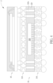
- FIG. 1 is a schematic, cross-sectional diagram showing an exemplary semiconductor package in accordance with an embodiment of the invention.
- the semiconductor package 1 may be a fan-out PoP, but is not limited thereto.
- the semiconductor package 1 may comprise a bottom package 10 and a top package 20 mounted on the bottom package 10.
- the bottom package 10 comprises an application processor (AP) die 100 surrounded by a molding compound 110.
- a dielectric layer DL may be disposed on an active surface 100 of the AP die 100.
- a plurality of conductive bumps or pillars 101 may be disposed in the dielectric layer DL and may be electrically coupled to the active surface 100a.
- the top surface S1 of the dielectric layer DL may be coplanar with the top surface S2 of the surrounding molding compound 110 after performing grinding or chemical mechanical polishing (CMP) process.
- CMP chemical mechanical polishing
- a re-distributed layer (RDL) structure RS may be disposed on the top surface S1 of the dielectric layer DL and the top surface S2 of the surrounding molding compound 110.
- the RDL structure RS may comprise multiple layers of interconnect IS.
- a plurality of ball pads PB may be distributed on the top surface S3 of the RDL structure RS.
- a solder ball SB may be mounted on each of the ball pads PB for further connection.
- a passive element PD such as a decoupling capacitor or any suitable surface mount devices (SMDs) may be disposed on the top surface S3 of the RDL structure RS among the solder balls SB.
- SMDs surface mount devices
- a plurality of through molding vias (TMVs) 110v is disposed in the molding compound 110 to electrically connect the RDL structure RS to the overlying re-distributed layer (RDL) structure RT.
- the RDL structure RT may at least comprise a plurality of bump pads PI and metal traces PT for connecting the bump pads PI with the TMVs 110v.
- the top package 20 is mounted on the bump pads PI through the bumps ST such as micro-bumps.
- the top package 20 may be a DRAM package such as a DDR DRAM package.
- the TMVs 110v may be interposer pillars or solder joints.
- FIG. 2 is a schematic diagram showing a partial top view layout of the TMVs 110v around the AP die 100 in FIG. 1 in accordance with an embodiment of the invention.
- each of the TMVs 110v may have an oval shape or a rectangular shape.
- Each of the TMVs 110v elongates along the second direction D2 or the via-to-die direction.
- the maximum length of each of the TMVs 110v is L and the maximum width of each of the TMVs 110v is W, wherein L is greater than W.
- the TMVs 110v in an exemplary 3x2 array may have a horizontal pitch P1 of W+ S h along the first direction D1 (i.e. the direction in parallel with an adjacent side edge of the AP die 100), wherein S h is the space between two neighboring TMVs 110v along the first direction D1.
- the TMVs 110v in a 3x2 array may have a vertical pitch P2 of L+ S v along the second direction D2, wherein S v is the space between two neighboring TMVs 110v along the second direction D2.
- the first direction D1 is orthogonal to the second direction D2.
- the vertical pitch P2 is greater than the horizontal pitch P1 of the TMVs 110v.
- TMVs 110v can be arranged around the AP die 100 in a more closely packed manner than the prior art.
- the connection length between the memory package 20 and the AP die 100 can be reduced because of the oval shaped TMV 110v, especially to those TMVs 100v disposed at a peripheral region or at an corner region of the semiconductor package 1.
- the two rows of the TMVs 110v may be aligned to each other in the second direction D2.
- the 3x2 array of the TMVs 110v may be staggered, that is, the front row is offset from the rear row.
- FIG. 4 illustrates an exemplary HBPoP.
- the HBPoP 2 has a bottom package 30 and a top package 40 such as a DRAM package mounted on the bottom package 30.
- the bottom package 30 comprises a top 2-layer substrate 310, a middle molding compound 320, and a bottom multi-layer substrate 330 to encapsulate an application processor (AP) die 300.
- AP application processor
- a plurality of TMVs 320v is disposed around the AP die 300.
- the TMVs 320v are disposed in the molding compound 320 and are used to electrically connect the top 2-layer substrate 310 with the bottom multi-layer substrate 330.
- the MVs 320v disposed in the middle molding compound electrically connect the top package with the AP die, wherein each of the plurality of TMVs has an oval shape, a rectangle shape or a combination thereof.
- FIG. 5 illustrates an exemplary semiconductor package.
- the semiconductor package 3 comprises an AP die 500 encapsulated by a molding compound 520 and surrounded by a via substrate 522 with a plurality of vias 522v.
- the AP die 500 and a memory device 600 such as a DRAM package are mounted on the substrate 530 in a side-by-side manner.
- a top bridge substrate 510 is disposed on the via substrate 522 and the molding compound 520.
- the signal path PP shows that the signal from the AP die 500 is transmitted through the substrate 530, the via substrate 522 and the vias 522v on the left side, the top bridge substrate 510, the via substrate 522 and the vias 522v on the right side, and the substrate 530 to the memory die 600.
- the rectangular-shaped or oval-shaped vias 522v as depicted in FIG. 2 and FIG. 3 can significantly improve the electrical performance of the semiconductor package 3 because the connection length of the signal transmission path PP can be reduced.
- FIG. 6 illustrates another exemplary semiconductor package.
- the semiconductor package 4 comprises a fan-out chip package 70 mounted on a substrate 80.
- the fan-out chip package 70 and a memory package 90 such as a DRAM package are mounted on the substrate in a side-by-side manner.
- the fan-out chip package 70 may comprise two logic dies 701 and 702 interconnected to a bridge via substrate 703 and a peripheral via structure 704 around the bridge via substrate 703.
- An RDL structure 705 is provided between the bridge via substrate 703 and the substrate 80 and between the peripheral via structure 704 and the substrate 80.
- the rectangular-shaped or oval-shaped vias 704v as depicted in FIG. 2 and FIG. 3 can significantly improve the electrical performance of the semiconductor package 4 because the connection length of the signal transmission path can be reduced.
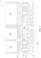
- FIG. 7 illustrates still another exemplary semiconductor package.
- the semiconductor package 5 may comprise logic dies 1001 and 1002, and a memory die 1003 interconnected through an RDL structure 1004.
- the RDL structure 1004 is further interconnected to a through-silicon-via (TSV) die 1005 surrounded by a molding compound 1006.
- TSV die 1005 comprises a plurality of through-silicon-vias 1005v penetrating through the TSV die 1005.
- a plurality of TMVs 1006v is disposed in the molding compound 1006 for signal transmission.
- the TMVs 1006v may be electrically connected to the TSV die 1005 through a bottom RDL structure 1007.
- the TSV die 1005 may be electrically connected to the logic dies 1001 and 1002, and the memory die 1003 through the bottom RDL structure 1007, the TMVs 1006v and the RDL structure 1004.
- the rectangular-shaped or oval-shaped vias 1006v as depicted in FIG. 2 and FIG. 3 can significantly improve the electrical performance of the semiconductor package 5 because the connection length of the signal transmission path can be reduced.
Landscapes
- Semiconductor Integrated Circuits (AREA)
- Control And Other Processes For Unpacking Of Materials (AREA)
- Physics & Mathematics (AREA)
- Geometry (AREA)
Applications Claiming Priority (2)
| Application Number | Priority Date | Filing Date | Title |
|---|---|---|---|
| US202163232710P | 2021-08-13 | 2021-08-13 | |
| US17/866,566 US20230050400A1 (en) | 2021-08-13 | 2022-07-18 | Semiconductor package with reduced connection length |
Publications (1)
| Publication Number | Publication Date |
|---|---|
| EP4135032A1 true EP4135032A1 (de) | 2023-02-15 |
Family
ID=83228923
Family Applications (1)
| Application Number | Title | Priority Date | Filing Date |
|---|---|---|---|
| EP22187769.9A Pending EP4135032A1 (de) | 2021-08-13 | 2022-07-29 | Halbleitergehäuse mit reduzierter verbindungslänge |
Country Status (4)
| Country | Link |
|---|---|
| US (1) | US20230050400A1 (de) |
| EP (1) | EP4135032A1 (de) |
| CN (1) | CN115706087B (de) |
| TW (1) | TWI824647B (de) |
Cited By (1)
| Publication number | Priority date | Publication date | Assignee | Title |
|---|---|---|---|---|
| US20230317561A1 (en) * | 2022-03-30 | 2023-10-05 | Intel Corporation | Scalable architecture for multi-die semiconductor packages |
Families Citing this family (2)
| Publication number | Priority date | Publication date | Assignee | Title |
|---|---|---|---|---|
| US12581971B2 (en) * | 2022-05-24 | 2026-03-17 | Mediatek Inc. | Semiconductor device with bridge die electrically connecting two chips and manufacturing method thereof |
| KR20260017015A (ko) * | 2024-07-16 | 2026-02-05 | 삼성전자주식회사 | 반도체 패키지 |
Citations (3)
| Publication number | Priority date | Publication date | Assignee | Title |
|---|---|---|---|---|
| US20140103527A1 (en) * | 2012-03-23 | 2014-04-17 | Stats Chippac, Ltd. | Semiconductor Device and Method of Forming a POP Device with Embedded Vertical Interconnect Units |
| US20160300817A1 (en) * | 2015-04-09 | 2016-10-13 | Stats Chippac, Ltd. | Semiconductor Device and Method of Forming a Package In-Fan Out Package |
| US20200194326A1 (en) * | 2018-03-20 | 2020-06-18 | Taiwan Semiconductor Manufacturing Co., Ltd. | Package, package-on-package structure, and method of manufacturing package-on-package structure |
Family Cites Families (9)
| Publication number | Priority date | Publication date | Assignee | Title |
|---|---|---|---|---|
| WO2015047330A1 (en) * | 2013-09-27 | 2015-04-02 | Intel Corporation | Die package with superposer substrate for passive components |
| US9318442B1 (en) * | 2014-09-29 | 2016-04-19 | Taiwan Semiconductor Manufacturing Company, Ltd. | Integrated fan-out package with dummy vias |
| TWI559419B (zh) * | 2015-08-21 | 2016-11-21 | 力成科技股份有限公司 | 使用模封互連基板製程之柱頂互連(pti)型態半導體封裝構造及其製造方法 |
| KR102384863B1 (ko) * | 2015-09-09 | 2022-04-08 | 삼성전자주식회사 | 반도체 칩 패키지 및 이의 제조 방법 |
| KR102109569B1 (ko) * | 2015-12-08 | 2020-05-12 | 삼성전자주식회사 | 전자부품 패키지 및 이를 포함하는 전자기기 |
| US9793230B1 (en) * | 2016-07-08 | 2017-10-17 | Taiwan Semiconductor Manufacturing Company, Ltd. | Semiconductor structure and method of forming |
| US20180047692A1 (en) * | 2016-08-10 | 2018-02-15 | Amkor Technology, Inc. | Method and System for Packing Optimization of Semiconductor Devices |
| US11450560B2 (en) * | 2018-09-24 | 2022-09-20 | Intel Corporation | Microelectronic assemblies having magnetic core inductors |
| US11887959B2 (en) * | 2020-12-17 | 2024-01-30 | Stmicroelectronics S.R.L. | Chip-on-lead semiconductor device, and corresponding method of manufacturing chip-on-lead semiconductor devices |
-
2022
- 2022-07-18 US US17/866,566 patent/US20230050400A1/en active Pending
- 2022-07-29 EP EP22187769.9A patent/EP4135032A1/de active Pending
- 2022-07-29 CN CN202210911081.5A patent/CN115706087B/zh active Active
- 2022-08-04 TW TW111129311A patent/TWI824647B/zh active
Patent Citations (3)
| Publication number | Priority date | Publication date | Assignee | Title |
|---|---|---|---|---|
| US20140103527A1 (en) * | 2012-03-23 | 2014-04-17 | Stats Chippac, Ltd. | Semiconductor Device and Method of Forming a POP Device with Embedded Vertical Interconnect Units |
| US20160300817A1 (en) * | 2015-04-09 | 2016-10-13 | Stats Chippac, Ltd. | Semiconductor Device and Method of Forming a Package In-Fan Out Package |
| US20200194326A1 (en) * | 2018-03-20 | 2020-06-18 | Taiwan Semiconductor Manufacturing Co., Ltd. | Package, package-on-package structure, and method of manufacturing package-on-package structure |
Cited By (1)
| Publication number | Priority date | Publication date | Assignee | Title |
|---|---|---|---|---|
| US20230317561A1 (en) * | 2022-03-30 | 2023-10-05 | Intel Corporation | Scalable architecture for multi-die semiconductor packages |
Also Published As
| Publication number | Publication date |
|---|---|
| CN115706087B (zh) | 2026-03-13 |
| CN115706087A (zh) | 2023-02-17 |
| US20230050400A1 (en) | 2023-02-16 |
| TW202308071A (zh) | 2023-02-16 |
| TWI824647B (zh) | 2023-12-01 |
Similar Documents
| Publication | Publication Date | Title |
|---|---|---|
| US12080615B2 (en) | Method of manufacturing an integrated fan-out package having fan-out redistribution layer (RDL) to accommodate electrical connectors | |
| US12293985B2 (en) | Integrated circuit packages and methods of forming the same | |
| US11171076B2 (en) | Compute-in-memory packages and methods forming the same | |
| US10181457B2 (en) | Microelectronic package for wafer-level chip scale packaging with fan-out | |
| US9496196B2 (en) | Packages and methods of manufacture thereof | |
| EP2775512B1 (de) | Halbleiterbauelemente | |
| EP4135032A1 (de) | Halbleitergehäuse mit reduzierter verbindungslänge | |
| US20180040587A1 (en) | Vertical Memory Module Enabled by Fan-Out Redistribution Layer | |
| US9099475B2 (en) | Techniques for reducing inductance in through-die vias of an electronic assembly | |
| US12021068B2 (en) | Semiconductor device with dummy thermal features on interposer | |
| US12166026B2 (en) | Semiconductor packages and methods for forming the same | |
| US12327777B2 (en) | Semiconductor package structure and manufacturing method thereof | |
| US12170275B2 (en) | Graphics processing unit and high bandwidth memory integration using integrated interface and silicon interposer | |
| US12394757B2 (en) | Semiconductor devices with redistribution structures configured for switchable routing | |
| US9343449B2 (en) | Alternative 3D stacking scheme for DRAMs atop GPUs | |
| US20250174576A1 (en) | Semiconductor package and fabrication method thereof | |
| US11145627B2 (en) | Semiconductor package and manufacturing method thereof | |
| KR20240166072A (ko) | 반도체 패키지 및 그 제조 방법 | |
| TWI703700B (zh) | 半導體封裝及其製造方法 | |
| CN112490129A (zh) | 半导体封装及其制造方法 | |
| KR20260031005A (ko) | 반도체 패키지 | |
| CN119815840A (zh) | 具有堆叠存储器和逻辑的半导体封装 | |
| KR20250159817A (ko) | 반도체 패키지 | |
| KR20250122817A (ko) | 반도체 패키지 및 이의 제조 방법 | |
| CN119725247A (zh) | 晶圆规模的系统级封装结构及其形成方法 |
Legal Events
| Date | Code | Title | Description |
|---|---|---|---|
| PUAI | Public reference made under article 153(3) epc to a published international application that has entered the european phase |
Free format text: ORIGINAL CODE: 0009012 |
|
| STAA | Information on the status of an ep patent application or granted ep patent |
Free format text: STATUS: THE APPLICATION HAS BEEN PUBLISHED |
|
| AK | Designated contracting states |
Kind code of ref document: A1 Designated state(s): AL AT BE BG CH CY CZ DE DK EE ES FI FR GB GR HR HU IE IS IT LI LT LU LV MC MK MT NL NO PL PT RO RS SE SI SK SM TR |
|
| P01 | Opt-out of the competence of the unified patent court (upc) registered |
Effective date: 20230607 |
|
| STAA | Information on the status of an ep patent application or granted ep patent |
Free format text: STATUS: REQUEST FOR EXAMINATION WAS MADE |
|
| 17P | Request for examination filed |
Effective date: 20230809 |
|
| RBV | Designated contracting states (corrected) |
Designated state(s): AL AT BE BG CH CY CZ DE DK EE ES FI FR GB GR HR HU IE IS IT LI LT LU LV MC MK MT NL NO PL PT RO RS SE SI SK SM TR |