EP4136052B1 - Procédé de production d'au moins un premier et un second dispositif de micro-miroir - Google Patents
Procédé de production d'au moins un premier et un second dispositif de micro-miroir Download PDFInfo
- Publication number
- EP4136052B1 EP4136052B1 EP21716282.5A EP21716282A EP4136052B1 EP 4136052 B1 EP4136052 B1 EP 4136052B1 EP 21716282 A EP21716282 A EP 21716282A EP 4136052 B1 EP4136052 B1 EP 4136052B1
- Authority
- EP
- European Patent Office
- Prior art keywords
- silicon
- layer
- separation region
- oxide layer
- silicon wafer
- Prior art date
- Legal status (The legal status is an assumption and is not a legal conclusion. Google has not performed a legal analysis and makes no representation as to the accuracy of the status listed.)
- Active
Links
Images


Classifications
-
- B—PERFORMING OPERATIONS; TRANSPORTING
- B81—MICROSTRUCTURAL TECHNOLOGY
- B81B—MICROSTRUCTURAL DEVICES OR SYSTEMS, e.g. MICROMECHANICAL DEVICES
- B81B3/00—Devices comprising flexible or deformable elements, e.g. comprising elastic tongues or membranes
- B81B3/0064—Constitution or structural means for improving or controlling the physical properties of a device
- B81B3/0067—Mechanical properties
- B81B3/007—For controlling stiffness, e.g. ribs
-
- B—PERFORMING OPERATIONS; TRANSPORTING
- B81—MICROSTRUCTURAL TECHNOLOGY
- B81B—MICROSTRUCTURAL DEVICES OR SYSTEMS, e.g. MICROMECHANICAL DEVICES
- B81B7/00—Microstructural systems ; Auxiliary parts of microstructural devices or systems
- B81B7/02—Microstructural systems ; Auxiliary parts of microstructural devices or systems containing distinct electrical or optical devices of particular relevance for their function, e.g. microelectro-mechanical systems [MEMS]
-
- B—PERFORMING OPERATIONS; TRANSPORTING
- B81—MICROSTRUCTURAL TECHNOLOGY
- B81C—PROCESSES OR APPARATUS SPECIALLY ADAPTED FOR THE MANUFACTURE OR TREATMENT OF MICROSTRUCTURAL DEVICES OR SYSTEMS
- B81C1/00—Manufacture or treatment of devices or systems in or on a substrate
- B81C1/00388—Etch mask forming
- B81C1/00404—Mask characterised by its size, orientation or shape
-
- B—PERFORMING OPERATIONS; TRANSPORTING
- B81—MICROSTRUCTURAL TECHNOLOGY
- B81C—PROCESSES OR APPARATUS SPECIALLY ADAPTED FOR THE MANUFACTURE OR TREATMENT OF MICROSTRUCTURAL DEVICES OR SYSTEMS
- B81C1/00—Manufacture or treatment of devices or systems in or on a substrate
- B81C1/00436—Shaping materials, i.e. techniques for structuring the substrate or the layers on the substrate
- B81C1/00555—Achieving a desired geometry, i.e. controlling etch rates, anisotropy or selectivity
- B81C1/00619—Forming high aspect ratio structures having deep steep walls
-
- B—PERFORMING OPERATIONS; TRANSPORTING
- B81—MICROSTRUCTURAL TECHNOLOGY
- B81C—PROCESSES OR APPARATUS SPECIALLY ADAPTED FOR THE MANUFACTURE OR TREATMENT OF MICROSTRUCTURAL DEVICES OR SYSTEMS
- B81C1/00—Manufacture or treatment of devices or systems in or on a substrate
- B81C1/00642—Manufacture or treatment of devices or systems in or on a substrate for improving the physical properties of a device
- B81C1/0065—Mechanical properties
- B81C1/00658—Treatments for improving the stiffness of a vibrating element
-
- B—PERFORMING OPERATIONS; TRANSPORTING
- B81—MICROSTRUCTURAL TECHNOLOGY
- B81B—MICROSTRUCTURAL DEVICES OR SYSTEMS, e.g. MICROMECHANICAL DEVICES
- B81B2201/00—Specific applications of microelectromechanical systems
- B81B2201/01—Switches
- B81B2201/012—Switches characterised by the shape
- B81B2201/014—Switches characterised by the shape having a cantilever fixed on one side connected to one or more dimples
-
- B—PERFORMING OPERATIONS; TRANSPORTING
- B81—MICROSTRUCTURAL TECHNOLOGY
- B81B—MICROSTRUCTURAL DEVICES OR SYSTEMS, e.g. MICROMECHANICAL DEVICES
- B81B2201/00—Specific applications of microelectromechanical systems
- B81B2201/04—Optical MEMS
- B81B2201/042—Micromirrors, not used as optical switches
-
- B—PERFORMING OPERATIONS; TRANSPORTING
- B81—MICROSTRUCTURAL TECHNOLOGY
- B81C—PROCESSES OR APPARATUS SPECIALLY ADAPTED FOR THE MANUFACTURE OR TREATMENT OF MICROSTRUCTURAL DEVICES OR SYSTEMS
- B81C2201/00—Manufacture or treatment of microstructural devices or systems
- B81C2201/01—Manufacture or treatment of microstructural devices or systems in or on a substrate
- B81C2201/0101—Shaping material; Structuring the bulk substrate or layers on the substrate; Film patterning
- B81C2201/0128—Processes for removing material
- B81C2201/013—Etching
- B81C2201/0135—Controlling etch progression
- B81C2201/014—Controlling etch progression by depositing an etch stop layer, e.g. silicon nitride, silicon oxide, metal
-
- B—PERFORMING OPERATIONS; TRANSPORTING
- B81—MICROSTRUCTURAL TECHNOLOGY
- B81C—PROCESSES OR APPARATUS SPECIALLY ADAPTED FOR THE MANUFACTURE OR TREATMENT OF MICROSTRUCTURAL DEVICES OR SYSTEMS
- B81C2201/00—Manufacture or treatment of microstructural devices or systems
- B81C2201/01—Manufacture or treatment of microstructural devices or systems in or on a substrate
- B81C2201/0198—Manufacture or treatment of microstructural devices or systems in or on a substrate for making a masking layer
-
- B—PERFORMING OPERATIONS; TRANSPORTING
- B81—MICROSTRUCTURAL TECHNOLOGY
- B81C—PROCESSES OR APPARATUS SPECIALLY ADAPTED FOR THE MANUFACTURE OR TREATMENT OF MICROSTRUCTURAL DEVICES OR SYSTEMS
- B81C2203/00—Forming microstructural systems
- B81C2203/03—Bonding two components
- B81C2203/033—Thermal bonding
Definitions
- the invention relates to a method for producing at least a first and a second micromirror device.
- the invention relates to a first and/or second micromirror device, produced by means of the method and a first and/or second micromirror device, in particular produced by means of a method according to one of claims 1 to 13, with a first and/or second mirror plate, each having a polysilicon layer.
- a method for producing micromirrors involves using a silicon oxide wafer, which is first separated along a separation plane in one process step using wet etching, and in a further, separate process step the mirror plates of the micromirrors are separated.
- micromirrors are known in which two etching steps, one from the front side and one from the back side of a substrate carrying thin film layers, are applied one after the other to form a micromirror.
- a method according to the invention is defined in claim 1.
- a micromirror device is hereby meant in particular a mechanical micromirror, i.e. a micromirror that is not yet connected to the drive unit of the Micromirror is connected.
- a silicon wafer in particular a plate-shaped one, is provided with a front side and a back side.
- the front side of the silicon wafer refers in particular to the side which, in the finished micromirror device, is aligned in the direction of the surface of the micromirror device which reflects incident light rays.
- a silicon oxide layer is thermally applied to at least the front side of the silicon wafer, in particular with a layer thickness of the silicon oxide layer in a range from 1 ⁇ m to 3 ⁇ m. In particular, the silicon oxide layer is applied with a layer thickness of 2 ⁇ m.
- the silicon oxide layer is removed, in particular up to an outer surface of the silicon wafer, in such a way that at least a first separation region and at least a second separation region of the silicon oxide layer are created. The first and second separation regions of the silicon oxide layer are spatially separated from one another, along a separation plane. Accordingly, there is no longer any material cohesion between the first and second separation regions of the silicon oxide layer.
- the separation plane is in particular a plane that is arranged essentially perpendicular to an outer surface of the silicon wafer.
- a silicon layer in particular a polysilicon layer with a layer thickness in a range from 5 ⁇ m to 50 ⁇ m, is applied to the front side of the silicon wafer and to the silicon oxide layer, in particular to the first and second separation region of the silicon oxide layer.
- the silicon layer is therefore in direct contact with the front side of the silicon wafer, in particular with an outer surface of the front side of the silicon wafer, and with the silicon oxide layer, in particular with an outer surface of the silicon oxide layer.
- an etching mask is applied to the back side of the silicon wafer, the etching mask having a first opening along the separation plane of the first and second separation region of the silicon oxide layer.
- the etching mask is in particular a hard mask or a resist mask.
- a further silicon oxide layer is applied to the back side of the silicon wafer as an etching mask.
- the silicon layer, in particular a part of the silicon layer, and the silicon wafer, in particular a part of the silicon wafer are then etched by means of an etching process depending on the etching mask on the back of the silicon wafer and depending on the silicon oxide layer of the silicon wafer, in particular the first and second Separation region of the silicon oxide layer, so that at least a first and a second micromirror device are produced.
- the etching mask, as well as the silicon oxide layer serve as layers that stop the etching (etch stop layers).
- first separation region and one second separation region of the silicon wafer are preferably produced.
- the first and second separation regions of the silicon wafer are arranged spatially separated from one another along the separation plane.
- a first stiffening structure of the first micromirror device comprising the first separation region of the silicon wafer and the first separation region of the silicon oxide layer
- a second stiffening structure of the second micromirror device comprising the second separation region of the silicon wafer and the second separation region of the silicon oxide layer
- the stiffening structure should have as little weight as possible in order to enable a high degree of mobility of the micromirror, and on the other hand, the stiffening structure of the mirror plate must also provide the necessary stability.
- the etching mask preferably also has at least one second opening, in particular for separating the first stiffening structure into a first separation region of the first stiffening structure and a second separation region of the first stiffening structure.
- the respective stiffening structure can thus be constructed as at least two stiffening struts running parallel to one another.
- a plasma etching process in particular the DRIE etching process, is used as the etching process.
- an ion beam etching process is used as the etching process.
- the mirror plate as well as the stiffening structure of a micromirror device can thus be produced in a single process step.
- the silicon wafer is provided as a raw wafer at the beginning of the process with a thickness of essentially 300 to 400 ⁇ m.
- the raw wafer already has a thickness at the beginning of the process which the stiffening structure in the finished micromirror device should have as a target thickness in order to meet the conditions with regard to weight and stability.
- the silicon wafer is provided as a raw wafer at the beginning of the process with a thickness of essentially 725 ⁇ m.
- the back side of the silicon wafer is ground down, in particular until a target thickness of the silicon wafer is reached.
- the target thickness corresponds in particular to a layer thickness in a range from 300 ⁇ m to 400 ⁇ m.
- the silicon oxide layer is additionally applied thermally to the back of the silicon wafer.
- the silicon oxide layer can be used, for example, as an etching mask on the back if the silicon wafer is provided as a raw wafer at the beginning of the process with a thickness of essentially 300 to 400 ⁇ m.
- a first metal layer in particular a first gold layer or a first aluminum layer
- a second metal layer in particular a second gold layer or a second aluminum layer
- the reflectance of the mirror plate of the respective micromirror device is thus increased.
- at least two markings are applied to the silicon layer to align the first metal layer relative to the first separation region of the silicon oxide layer and to align the second metal layer relative to the at least second separation region of the silicon oxide layer. The at least two markings are etched in particular into an outer surface of the silicon layer.
- an infrared measuring device is used in particular, by means of which the structure of the first separation region and the at least second separation region of the silicon oxide layer buried within the layer stack can be detected.
- the at least two markings are then applied in particular to an edge region of the layer stack.
- the metal layers on the front side of the silicon wafer can be aligned with the structure of the first separation region and the at least second separation region of the silicon oxide layer buried within the layer structure.
- the silicon layer in particular an outer surface of the first separation region of the silicon layer and an outer surface of the second separation region of the silicon layer, is also directly or indirectly connected to an adhesive tape, in particular a single-sided adhesive tape.
- the adhesive tape which can be designed in particular as a blue tape, serves on the one hand to transport the finished first and second micromirror device to the respective drive unit of the micromirror and on the other hand to stop the etching process in which part of the silicon layer and the silicon wafer is removed.
- the etching mask is removed in a further process step.
- the etching mask is a resist mask
- the etching mask is removed, for example, by means of a plasma strip.
- the etching mask can be removed using an oxide etching process. If an oxide etching process is used, the exposed parts of the silicon oxide layer on the front side of the silicon wafer are also etched away. This allows the pressure of the stiffening structure on the mirror plate to be reduced.
- the silicon layer is applied in the form of a deposition of silicon, in particular polysilicon, on the front side of the silicon wafer and on the silicon oxide layer, in particular on the first and second separation region of the silicon oxide layer, and a subsequent polishing step.
- silicon in particular polysilicon
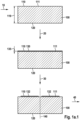
- Figure 1a.1 to 1a.3 show schematically the method steps of a first embodiment of a method for producing at least a first and a second micromirror device.
- a silicon wafer 100 in particular a plate-shaped one, with a front side 110 and a back side 120 is provided.
- a silicon oxide layer 130 is applied to the front side 110 of the silicon wafer 100, in particular with a layer thickness 135 of the silicon oxide layer 130 of essentially 2 ⁇ m.
- the silicon oxide layer 130 is removed, in particular up to an outer surface 111 of the silicon wafer 100, in such a way that a first separation region 131 and a second separation region 132 of the silicon oxide layer 130 are produced.
- the first 131 and the second separation region 132 of the silicon oxide layer 130 are arranged spatially separated from one another along a separation plane 140.
- a silicon layer 150 in particular with a layer thickness 116 of essentially 20 ⁇ m, is applied to the front side 110 of the silicon wafer 100 and to the first 131 and second separation region 132 of the silicon oxide layer 130.
- the silicon layer 150 is a polysilicon layer.
- an etching mask 180 is applied to the back side 120 of the silicon wafer 100.
- the etching mask 180 has a first opening 190 along the separation plane 140.
- the etching mask 180 is a hard mask which is formed from a further silicon oxide layer 181 and is applied to the back side 120 of the silicon wafer.
- the silicon layer 150, in particular a part of the silicon layer 150, and the silicon wafer 100, in particular a part of the silicon wafer 100 are then removed by means of an etching process depending on the etching mask 180 on the back side 120 of the silicon wafer 100 and depending on the first 131 and second separation region 132 of the silicon oxide layer 130, so that at least a first 205 and a second micromirror device 206 are produced.
- the first 131 and second separation region 132 of the silicon oxide layer 130 are formed as etching stop layers.
- At least one first separation region 200 and one second separation region 201 of the silicon layer 150 are produced by removing the silicon layer 150 by means of the etching process in method step 80.
- the first 200 and the second separation region 201 of the silicon layer 150 are also arranged spatially separated from one another along the separation plane 140.
- a first mirror plate 211 of the first micromirror device 205, having the first separation region 200 of the silicon layer 150, and a second mirror plate 212 of the second micromirror device 206, having the second separation region 201 of the silicon layer 150 are produced.
- a first separation region and a second separation region of the silicon wafer 100 are produced by removing the silicon wafer 100 by means of the etching process in method step 80.
- the first and second separation regions of the silicon wafer 100 are arranged spatially separated from one another along the separation plane 140.
- the etching mask 180 has a second 221, third 222, fourth 223 and fifth opening 224. These openings are designed to separate the first 195 and second stiffening structure 196 into further separation regions, which in this embodiment are designed as first 231, second 232, third 233, fourth 234, fifth 235 and sixth 236 stiffening struts.
- a plasma etching method in particular the DRIE etching method, is used as the etching method in method step 80.
- the silicon wafer 100 with a thickness 119 of substantially 300 to 400 ⁇ m is provided in method step 10.
- a first metal layer 170 is applied to an outer surface 151 of the silicon layer 150.
- the first metal layer is formed as a gold layer and this gold layer is applied to a region of the silicon layer 150 which later corresponds to the first separation region 200 of the silicon layer 150.
- a second metal layer 171 is applied to an outer surface 151 of the silicon layer 150.
- the second metal layer 171 is formed as a gold layer and this gold layer is applied to a region of the silicon layer 150 which later corresponds to the second separation region 201 of the silicon layer 150.
- two markings 160 and 161 are applied to the silicon layer 150.
- the two markings 160 and 161 are etched into an outer surface 151 of the silicon layer 150. These markings 160 and 161 serve to align the first metal layer 17) relative to the first separation region 131 of the silicon oxide layer 130 and to align the second metal layer 171 relative to the at least second separation region 132 of the silicon oxide layer.
- an infrared measuring device (not shown here) is used, by means of which the first separation region 131 and second separation region 132 of the silicon oxide layer 130 buried within the layer stack comprising the silicon wafer 100 and the silicon layer can be detected. The two markings 131 and 132 are then applied in particular to an edge region of the layer stack.
- an outer surface 152 of the first separating region 200 of the silicon layer 150 and an outer surface 153 of the second separating region 201 of the silicon layer are indirectly connected to an adhesive tape 220.
- the first 170 and second metal layer 171 are directly bonded to the adhesive tape 220.
- the adhesive tape 220 serves on the one hand as an etching stop layer during the etching process in method step 80.
- the adhesive tape 220 which is designed in particular as a one-sided adhesive tape, serves to hold the finished manufactured first and second micromirror devices to the respective drive unit, in particular piezoelectric drive unit, of the micromirror (not shown here).
- the etching mask 180 which is designed as a hard mask, is removed by means of an oxide etching process.
- the exposed regions 241 of the first separation region 131 of the silicon oxide layer 130 and the exposed regions 242 of the second separation region 132 of the silicon oxide layer 130 are also etched away.
- Au f Figures 1b.1 to 1b.4 the method steps of a second embodiment of a method for producing at least a first and a second micromirror device are shown schematically.
- a silicon wafer 101 with a thickness 126 of essentially 725 ⁇ m is provided in contrast to the first embodiment.
- a silicon oxide layer 130 is not only applied to the front side 110 of the silicon wafer 101, but also to the back side 120 of the silicon wafer 101.
- the back side 120 of the silicon wafer 101 is ground down until a target thickness 145 of the silicon wafer 101 is reached.
- the target thickness 145 corresponds to a thickness of the silicon wafer 101 of essentially 300 ⁇ m to 400 ⁇ m.
Landscapes
- Engineering & Computer Science (AREA)
- Microelectronics & Electronic Packaging (AREA)
- Manufacturing & Machinery (AREA)
- Computer Hardware Design (AREA)
- Physics & Mathematics (AREA)
- Geometry (AREA)
- Mechanical Engineering (AREA)
- Micromachines (AREA)
Claims (14)
- Procédé de fabrication d'au moins un premier (205, 300) et un deuxième (206) dispositif à micro-miroir, le procédé comprenant les étapes suivantes :- prévoir (10, 11) une tranche de silicium (100, 101), en particulier en forme de plaque, ayant une face avant (110) et une face arrière (120), et- appliquer (20) une couche d'oxyde de silicium (130) sur au moins la face avant (110) de la tranche de silicium (100, 101), en particulier avec une épaisseur de couche (135) de la couche d'oxyde de silicium (130) située dans une gamme allant de 1µm à 3µm, et- éliminer (30) la couche d'oxyde de silicium (130), en particulier jusqu'à une surface extérieure (111) de la tranche de silicium (100, 101), de telle sorte qu'au moins une première zone de séparation (131) et au moins une deuxième zone de séparation (132) de la couche d'oxyde de silicium (130) soient produites, la première (131) et la deuxième zone de séparation (132) de la couche d'oxyde de silicium (130) étant aménagées de façon spatialement séparée l'une de l'autre, le long d'un plan de séparation (140), et- appliquer (40) une couche de silicium (150, 350), en particulier d'une couche de polysilicium ayant une épaisseur de couche (116) située dans une gamme allant de 5µm à 50µm, sur la face avant (110) de la tranche de silicium (100, 101) et sur la couche d'oxyde de silicium (130), en particulier sur la première (131) et la deuxième zone de séparation (132) de la couche d'oxyde de silicium (130), et- appliquer (70) un masque de gravure (180) sur la face arrière (120) de la tranche de silicium (100), le masque de gravure (180) présentant une première ouverture (190) le long du plan de séparation (140) de la première (131) et de la deuxième (132) zone de séparation de la couche d'oxyde de silicium (130), et- éliminer (80) la couche de silicium (150, 350) et la tranche de silicium (100, 101) au moyen d'un procédé de gravure en une étape de procédé en fonction du masque de gravure (180) sur la face arrière (120) de la tranche de silicium (100, 101) et en fonction de la couche d'oxyde de silicium (130) de la tranche de silicium (100, 101), en particulier des première (131) et deuxième (132) zones de séparation de la couche d'oxyde de silicium (130), de sorte qu'au moins un premier (205, 300) et un deuxième dispositif à micro-miroir (206) soient produits.
- Procédé selon la revendication 1, caractérisé en ce que, par l'élimination (80) de la couche de silicium (150, 350) au moyen du procédé de gravure, il est produit au moins une première zone de séparation (200, 345) et une deuxième zone de séparation (201) de la couche de silicium (150, 350), la première (200) et la deuxième (201) zone de séparation de la couche de silicium (150, 350) étant aménagées de façon spatialement espacée l'une de l'autre, le long du plan de séparation (140), créant ainsi une première plaque miroir (211, 320) du premier dispositif à micro-miroir (205, 300), comprenant la première zone de séparation (200, 345) de la couche de silicium (150, 350), et une deuxième plaque miroir (212) du deuxième dispositif à micro-miroir (206), comprenant la deuxième zone de séparation (201) de la couche de silicium (150, 350).
- Procédé selon l'une des revendications 1 ou 2, caractérisé en ce que, par l'élimination (80) de la tranche de silicium (100, 101) au moyen du procédé de gravure, il est généré au moins une première zone de séparation et une deuxième zone de séparation de la tranche de silicium (100, 101), la première et la deuxième zone de séparation de la tranche de silicium (100, 101) étant aménagées de façon spatialement séparée l'une de l'autre le long du plan de séparation, une première structure de renforcement (195, 310) du premier dispositif à micro-miroir (205, 300), comprenant la première zone de séparation de la tranche de silicium (100, 101) et la première zone de séparation (131) de la couche d'oxyde de silicium (130), et une deuxième structure de renforcement (196) du deuxième dispositif à micro-miroir (206), comprenant la deuxième zone de séparation de la tranche de silicium (100, 101) et la deuxième zone de séparation de la couche d'oxyde de silicium (100, 101), étant ainsi générées.
- Procédé selon la revendication 3, caractérisé en ce que le masque de gravure (180) comporte au moins une deuxième ouverture (221), notamment pour séparer la première structure de rigidification (195, 310) en une première zone de séparation, notamment une première entretoise de rigidification (231, 311) de la première structure de rigidification (195, 310) et une deuxième zone de séparation, notamment une deuxième entretoise de rigidification (232, 312) de la première structure de rigidification (195, 310).
- Procédé selon l'une des revendications 1 à 4, caractérisé en ce que le procédé de gravure utilisé est un procédé de gravure par plasma, notamment le procédé de gravure DRIE.
- Procédé selon l'une des revendications 1 à 5, caractérisé en ce que la tranche de silicium (100) est fournie (10) avec une épaisseur (119) sensiblement comprise entre 300 et 400µm.
- Procédé selon l'une des revendications 1 à 5, caractérisé en ce que la tranche de silicium (101) est prévue (11) avec une épaisseur (126) sensiblement égale à 725µm.
- Procédé selon la revendication 7, caractérisé en ce que, dans une autre étape du procédé, notamment consécutive au dépôt (60) de la couche de silicium (150, 350), notamment de la couche de polysilicium, sur la face avant (110) de la tranche de silicium (100, 101) et sur la couche d'oxyde de silicium (130), la face arrière (120) de la tranche de silicium (100, 101) est meulée (65), notamment jusqu'à atteindre une épaisseur cible (145) de la tranche de silicium (100, 101).
- Procédé selon l'une des revendications 1 à 8, caractérisé en ce que la couche d'oxyde de silicium (130) est en outre appliquée (20) sur la face arrière (120) de la tranche de silicium (100, 101).
- Procédé selon l'une des revendications 1 à 9, caractérisé en ce que, dans une étape supplémentaire du procédé, une première couche métallique (170), en particulier une première couche d'or ou une première couche d'aluminium, est appliquée sur la couche de silicium (150, 350), en particulier sur une surface extérieure (152) de la première zone de séparation (200, 345) de la couche de silicium (150, 350), et une deuxième couche métallique (171), notamment une deuxième couche d'or ou une deuxième couche d'aluminium, est appliquée (60) sur la couche de silicium (150, 350), notamment sur une surface extérieure (153) de la deuxième zone de séparation (201) de la couche de silicium (150, 350).
- Procédé selon la revendication 10, caractérisé en ce que procédé selon l'une des revendications 1 à 9, caractérisé en ce que, pour aligner la première couche métallique (170) par rapport à la première zone de séparation (131) de la couche d'oxyde de silicium (130) et pour aligner la deuxième couche métallique (171) par rapport à au moins la deuxième zone de séparation (132) de la couche d'oxyde de silicium (130), au moins deux repères (160, 161) sont déposés sur la couche de silicium (150, 350).
- Procédé selon l'une des revendications 1 à 11, caractérisé en ce que la couche de silicium (150, 350), notamment la surface extérieure (152) de la première zone de séparation (200, 345) de la couche de silicium (150, 350) et la surface extérieure (153) de la deuxième zone de séparation (201) de la couche de silicium (150, 350), est liée directement ou indirectement par un ruban adhésif (220), notamment un ruban adhésif simple face.
- Procédé selon l'une des revendications 1 à 12, caractérisé en ce que, dans une autre étape du procédé, le masque de gravure (180) est retiré (90).
- Procédé selon l'une des revendications 1 à 13, caractérisé en ce que la couche de silicium (150, 350) est appliquée sous forme d'un dépôt de silicium, notamment de polysilicium, sur la face avant (110) de la tranche de silicium (100, 101) et sur la couche d'oxyde de silicium (130), notamment sur les première (131) et deuxième (132) zones de séparation de la couche d'oxyde de silicium (130), et une étape de polissage, notamment du silicium appliqué.
Applications Claiming Priority (2)
| Application Number | Priority Date | Filing Date | Title |
|---|---|---|---|
| DE102020204910.6A DE102020204910A1 (de) | 2020-04-17 | 2020-04-17 | Verfahren zur Herstellung von wenigstens einer ersten und einer zweiten Mikrospiegelvorrichtung |
| PCT/EP2021/057719 WO2021209238A1 (fr) | 2020-04-17 | 2021-03-25 | Procédé de production d'au moins un premier et un second dispositif de micro-miroir |
Publications (2)
| Publication Number | Publication Date |
|---|---|
| EP4136052A1 EP4136052A1 (fr) | 2023-02-22 |
| EP4136052B1 true EP4136052B1 (fr) | 2025-03-05 |
Family
ID=75377717
Family Applications (1)
| Application Number | Title | Priority Date | Filing Date |
|---|---|---|---|
| EP21716282.5A Active EP4136052B1 (fr) | 2020-04-17 | 2021-03-25 | Procédé de production d'au moins un premier et un second dispositif de micro-miroir |
Country Status (5)
| Country | Link |
|---|---|
| US (1) | US12570522B2 (fr) |
| EP (1) | EP4136052B1 (fr) |
| CN (1) | CN115427345B (fr) |
| DE (1) | DE102020204910A1 (fr) |
| WO (1) | WO2021209238A1 (fr) |
Families Citing this family (1)
| Publication number | Priority date | Publication date | Assignee | Title |
|---|---|---|---|---|
| CN119803736A (zh) * | 2023-10-10 | 2025-04-11 | 华润微电子控股有限公司 | 一种mems差分电容式压力传感器及其制造方法 |
Family Cites Families (12)
| Publication number | Priority date | Publication date | Assignee | Title |
|---|---|---|---|---|
| US8691099B2 (en) | 2001-12-13 | 2014-04-08 | John Gritters | Process for fabricating MEMS devices |
| JP4150003B2 (ja) * | 2003-04-25 | 2008-09-17 | 富士通株式会社 | マイクロ構造体の製造方法およびマイクロ構造体 |
| CN1813489A (zh) * | 2003-05-26 | 2006-08-02 | 森斯费伯私人有限公司 | 硅麦克风的制造 |
| US7091057B2 (en) | 2003-12-19 | 2006-08-15 | Agency For Science, Technology And Research | Method of making a single-crystal-silicon 3D micromirror |
| DE102008041178B4 (de) | 2008-08-12 | 2018-11-15 | Robert Bosch Gmbh | Herstellungsverfahren für ein mikromechanisches Bauteil |
| JP5773624B2 (ja) * | 2010-01-08 | 2015-09-02 | キヤノン株式会社 | 微細構造体の製造方法 |
| US8636911B2 (en) * | 2010-10-07 | 2014-01-28 | Magic Technologies, Inc. | Process for MEMS scanning mirror with mass remove from mirror backside |
| JP5939752B2 (ja) * | 2011-09-01 | 2016-06-22 | 株式会社ディスコ | ウェーハの分割方法 |
| JP6046443B2 (ja) * | 2012-10-19 | 2016-12-14 | 国立大学法人東北大学 | マイクロミラーデバイスの製造方法 |
| KR20150063540A (ko) | 2012-10-23 | 2015-06-09 | 애플 인크. | 마이크로 기계 디바이스의 제조 |
| US9499399B2 (en) * | 2013-06-14 | 2016-11-22 | United Microelectronics Corp. | Method for forming MEMS structure with an etch stop layer buried within inter-dielectric layer |
| CN109160481B (zh) * | 2018-08-03 | 2020-07-07 | 南京理工大学 | 基于mems工艺的二维磁驱动扫描微镜及其制备方法 |
-
2020
- 2020-04-17 DE DE102020204910.6A patent/DE102020204910A1/de active Pending
-
2021
- 2021-03-25 EP EP21716282.5A patent/EP4136052B1/fr active Active
- 2021-03-25 WO PCT/EP2021/057719 patent/WO2021209238A1/fr not_active Ceased
- 2021-03-25 US US17/793,606 patent/US12570522B2/en active Active
- 2021-03-25 CN CN202180029195.0A patent/CN115427345B/zh active Active
Also Published As
| Publication number | Publication date |
|---|---|
| CN115427345B (zh) | 2026-02-10 |
| WO2021209238A1 (fr) | 2021-10-21 |
| DE102020204910A1 (de) | 2021-10-21 |
| CN115427345A (zh) | 2022-12-02 |
| US12570522B2 (en) | 2026-03-10 |
| US20230066345A1 (en) | 2023-03-02 |
| EP4136052A1 (fr) | 2023-02-22 |
Similar Documents
| Publication | Publication Date | Title |
|---|---|---|
| DE60316575T2 (de) | Verfahren und vorrichtung zum aufnehmen von halbleiterchips sowie dazu verwendbares saugung ablöswerkzeug | |
| DE60131111T2 (de) | Herstellungsverfahren eines Flüssigkristallanzeigesubstrats | |
| DE10051890A1 (de) | Halbleiterwaferteilungsverfahren | |
| DE102010002344A1 (de) | Abscheidungsmaske | |
| EP0723670B1 (fr) | Procede de fabrication de prismes, notamment de microprismes et de separateurs de rayonnement | |
| WO2010121703A1 (fr) | Procédé et dispositif utilisés pour séparer un substrat d'un substrat support | |
| EP4136052B1 (fr) | Procédé de production d'au moins un premier et un second dispositif de micro-miroir | |
| DE19934174C1 (de) | Verfahren zur Herstellung einer Torsionsfeder | |
| DE102010062009B4 (de) | Verfahren zum Herstellen von Schrägflächen in einem Substrat und Wafer mit Schrägfläche | |
| DE102014202842B4 (de) | Verfahren zum Herstellen eines mikromechanischen Bauteils | |
| DE60213317T2 (de) | Optisches Bauteil mit Handhabungseinrichtung, Verfahren zu dessen Herstellung und Befestigung sowie optisches Modul | |
| EP1359593A1 (fr) | Capteur pour la SPM et procedé pour sa fabrication | |
| DE102014211555A1 (de) | Verfahren zum Ausbilden einer Kavität und Bauelement mit einer Kavität | |
| EP2104111A1 (fr) | Sonde pour SPM avec un porte-à-faux raccourci | |
| DE4207951C2 (de) | Kapazitiver Druck- oder Differenzdrucksensor in Glas-Silizium-Technik | |
| EP1322947B1 (fr) | Procede pour la production d'une microcuve a circulation tridimensionnelle et microcuve a circulation tridimensionnelle | |
| EP2855131A1 (fr) | Procédé et dispositif de fabrication d'une pluralité de microlentilles | |
| DE60101134T2 (de) | Band aus einkritallinem Silizium für Mikrospiegel und MEMS auf SOI Material | |
| DE102023204321A1 (de) | Verfahren zum Herstellen eines mikroelektromechanischen Bauteils und mikroelektromechanisches Bauteil | |
| WO2008152151A2 (fr) | Dépôt de couche structuré sur plaquettes traitées en technologie des microsystèmes | |
| DE202014011175U1 (de) | Vorrichtung mit Ausrichtungsmerkmalen | |
| DE10026974A1 (de) | Kanalplatte aus Glas für Flachbildschirme und Verfahren zu ihrer Herstellung | |
| DE102019208023B4 (de) | Verfahren zum herstellen einer mikromechanischen vorrichtung, mikromechanisches ventil und mikropumpe | |
| EP3886149A1 (fr) | Dispositif et procédé de liaison de substrats | |
| DE102023201829A1 (de) | Herstellungsverfahren für eine mikromechanische Vorrichtung mit wenigstens einem geneigten optischen Fenster |
Legal Events
| Date | Code | Title | Description |
|---|---|---|---|
| STAA | Information on the status of an ep patent application or granted ep patent |
Free format text: STATUS: UNKNOWN |
|
| STAA | Information on the status of an ep patent application or granted ep patent |
Free format text: STATUS: THE INTERNATIONAL PUBLICATION HAS BEEN MADE |
|
| PUAI | Public reference made under article 153(3) epc to a published international application that has entered the european phase |
Free format text: ORIGINAL CODE: 0009012 |
|
| STAA | Information on the status of an ep patent application or granted ep patent |
Free format text: STATUS: REQUEST FOR EXAMINATION WAS MADE |
|
| 17P | Request for examination filed |
Effective date: 20221117 |
|
| AK | Designated contracting states |
Kind code of ref document: A1 Designated state(s): AL AT BE BG CH CY CZ DE DK EE ES FI FR GB GR HR HU IE IS IT LI LT LU LV MC MK MT NL NO PL PT RO RS SE SI SK SM TR |
|
| P01 | Opt-out of the competence of the unified patent court (upc) registered |
Effective date: 20230509 |
|
| DAV | Request for validation of the european patent (deleted) | ||
| DAX | Request for extension of the european patent (deleted) | ||
| GRAP | Despatch of communication of intention to grant a patent |
Free format text: ORIGINAL CODE: EPIDOSNIGR1 |
|
| STAA | Information on the status of an ep patent application or granted ep patent |
Free format text: STATUS: GRANT OF PATENT IS INTENDED |
|
| INTG | Intention to grant announced |
Effective date: 20241205 |
|
| GRAS | Grant fee paid |
Free format text: ORIGINAL CODE: EPIDOSNIGR3 |
|
| GRAA | (expected) grant |
Free format text: ORIGINAL CODE: 0009210 |
|
| STAA | Information on the status of an ep patent application or granted ep patent |
Free format text: STATUS: THE PATENT HAS BEEN GRANTED |
|
| AK | Designated contracting states |
Kind code of ref document: B1 Designated state(s): AL AT BE BG CH CY CZ DE DK EE ES FI FR GB GR HR HU IE IS IT LI LT LU LV MC MK MT NL NO PL PT RO RS SE SI SK SM TR |
|
| REG | Reference to a national code |
Ref country code: GB Ref legal event code: FG4D Free format text: NOT ENGLISH |
|
| REG | Reference to a national code |
Ref country code: CH Ref legal event code: EP |
|
| REG | Reference to a national code |
Ref country code: DE Ref legal event code: R096 Ref document number: 502021006860 Country of ref document: DE |
|
| REG | Reference to a national code |
Ref country code: IE Ref legal event code: FG4D Free format text: LANGUAGE OF EP DOCUMENT: GERMAN |
|
| PGFP | Annual fee paid to national office [announced via postgrant information from national office to epo] |
Ref country code: AT Payment date: 20250417 Year of fee payment: 5 |
|
| PG25 | Lapsed in a contracting state [announced via postgrant information from national office to epo] |
Ref country code: RS Free format text: LAPSE BECAUSE OF FAILURE TO SUBMIT A TRANSLATION OF THE DESCRIPTION OR TO PAY THE FEE WITHIN THE PRESCRIBED TIME-LIMIT Effective date: 20250605 |
|
| PG25 | Lapsed in a contracting state [announced via postgrant information from national office to epo] |
Ref country code: FI Free format text: LAPSE BECAUSE OF FAILURE TO SUBMIT A TRANSLATION OF THE DESCRIPTION OR TO PAY THE FEE WITHIN THE PRESCRIBED TIME-LIMIT Effective date: 20250305 |
|
| PGFP | Annual fee paid to national office [announced via postgrant information from national office to epo] |
Ref country code: DE Payment date: 20250522 Year of fee payment: 5 |
|
| REG | Reference to a national code |
Ref country code: NL Ref legal event code: MP Effective date: 20250305 |
|
| PG25 | Lapsed in a contracting state [announced via postgrant information from national office to epo] |
Ref country code: ES Free format text: LAPSE BECAUSE OF FAILURE TO SUBMIT A TRANSLATION OF THE DESCRIPTION OR TO PAY THE FEE WITHIN THE PRESCRIBED TIME-LIMIT Effective date: 20250305 |
|
| REG | Reference to a national code |
Ref country code: LT Ref legal event code: MG9D |
|
| PG25 | Lapsed in a contracting state [announced via postgrant information from national office to epo] |
Ref country code: NO Free format text: LAPSE BECAUSE OF FAILURE TO SUBMIT A TRANSLATION OF THE DESCRIPTION OR TO PAY THE FEE WITHIN THE PRESCRIBED TIME-LIMIT Effective date: 20250605 |
|
| PG25 | Lapsed in a contracting state [announced via postgrant information from national office to epo] |
Ref country code: HR Free format text: LAPSE BECAUSE OF FAILURE TO SUBMIT A TRANSLATION OF THE DESCRIPTION OR TO PAY THE FEE WITHIN THE PRESCRIBED TIME-LIMIT Effective date: 20250305 |
|
| PG25 | Lapsed in a contracting state [announced via postgrant information from national office to epo] |
Ref country code: LV Free format text: LAPSE BECAUSE OF FAILURE TO SUBMIT A TRANSLATION OF THE DESCRIPTION OR TO PAY THE FEE WITHIN THE PRESCRIBED TIME-LIMIT Effective date: 20250305 |
|
| PG25 | Lapsed in a contracting state [announced via postgrant information from national office to epo] |
Ref country code: GR Free format text: LAPSE BECAUSE OF FAILURE TO SUBMIT A TRANSLATION OF THE DESCRIPTION OR TO PAY THE FEE WITHIN THE PRESCRIBED TIME-LIMIT Effective date: 20250606 Ref country code: BG Free format text: LAPSE BECAUSE OF FAILURE TO SUBMIT A TRANSLATION OF THE DESCRIPTION OR TO PAY THE FEE WITHIN THE PRESCRIBED TIME-LIMIT Effective date: 20250305 |
|
| PG25 | Lapsed in a contracting state [announced via postgrant information from national office to epo] |
Ref country code: NL Free format text: LAPSE BECAUSE OF FAILURE TO SUBMIT A TRANSLATION OF THE DESCRIPTION OR TO PAY THE FEE WITHIN THE PRESCRIBED TIME-LIMIT Effective date: 20250305 |
|
| PG25 | Lapsed in a contracting state [announced via postgrant information from national office to epo] |
Ref country code: SE Free format text: LAPSE BECAUSE OF FAILURE TO SUBMIT A TRANSLATION OF THE DESCRIPTION OR TO PAY THE FEE WITHIN THE PRESCRIBED TIME-LIMIT Effective date: 20250305 |
|
| PG25 | Lapsed in a contracting state [announced via postgrant information from national office to epo] |
Ref country code: SM Free format text: LAPSE BECAUSE OF FAILURE TO SUBMIT A TRANSLATION OF THE DESCRIPTION OR TO PAY THE FEE WITHIN THE PRESCRIBED TIME-LIMIT Effective date: 20250305 |
|
| PG25 | Lapsed in a contracting state [announced via postgrant information from national office to epo] |
Ref country code: PT Free format text: LAPSE BECAUSE OF FAILURE TO SUBMIT A TRANSLATION OF THE DESCRIPTION OR TO PAY THE FEE WITHIN THE PRESCRIBED TIME-LIMIT Effective date: 20250707 |
|
| PG25 | Lapsed in a contracting state [announced via postgrant information from national office to epo] |
Ref country code: IT Free format text: LAPSE BECAUSE OF FAILURE TO SUBMIT A TRANSLATION OF THE DESCRIPTION OR TO PAY THE FEE WITHIN THE PRESCRIBED TIME-LIMIT Effective date: 20250305 Ref country code: PL Free format text: LAPSE BECAUSE OF FAILURE TO SUBMIT A TRANSLATION OF THE DESCRIPTION OR TO PAY THE FEE WITHIN THE PRESCRIBED TIME-LIMIT Effective date: 20250305 |
|
| PG25 | Lapsed in a contracting state [announced via postgrant information from national office to epo] |
Ref country code: EE Free format text: LAPSE BECAUSE OF FAILURE TO SUBMIT A TRANSLATION OF THE DESCRIPTION OR TO PAY THE FEE WITHIN THE PRESCRIBED TIME-LIMIT Effective date: 20250305 Ref country code: CZ Free format text: LAPSE BECAUSE OF FAILURE TO SUBMIT A TRANSLATION OF THE DESCRIPTION OR TO PAY THE FEE WITHIN THE PRESCRIBED TIME-LIMIT Effective date: 20250305 |
|
| REG | Reference to a national code |
Ref country code: CH Ref legal event code: H13 Free format text: ST27 STATUS EVENT CODE: U-0-0-H10-H13 (AS PROVIDED BY THE NATIONAL OFFICE) Effective date: 20251023 |
|
| PG25 | Lapsed in a contracting state [announced via postgrant information from national office to epo] |
Ref country code: RO Free format text: LAPSE BECAUSE OF FAILURE TO SUBMIT A TRANSLATION OF THE DESCRIPTION OR TO PAY THE FEE WITHIN THE PRESCRIBED TIME-LIMIT Effective date: 20250305 |
|
| PG25 | Lapsed in a contracting state [announced via postgrant information from national office to epo] |
Ref country code: SK Free format text: LAPSE BECAUSE OF FAILURE TO SUBMIT A TRANSLATION OF THE DESCRIPTION OR TO PAY THE FEE WITHIN THE PRESCRIBED TIME-LIMIT Effective date: 20250305 |
|
| PG25 | Lapsed in a contracting state [announced via postgrant information from national office to epo] |
Ref country code: IS Free format text: LAPSE BECAUSE OF FAILURE TO SUBMIT A TRANSLATION OF THE DESCRIPTION OR TO PAY THE FEE WITHIN THE PRESCRIBED TIME-LIMIT Effective date: 20250705 |
|
| PG25 | Lapsed in a contracting state [announced via postgrant information from national office to epo] |
Ref country code: LU Free format text: LAPSE BECAUSE OF NON-PAYMENT OF DUE FEES Effective date: 20250325 |
|
| REG | Reference to a national code |
Ref country code: DE Ref legal event code: R097 Ref document number: 502021006860 Country of ref document: DE |
|
| REG | Reference to a national code |
Ref country code: BE Ref legal event code: MM Effective date: 20250331 |
|
| PG25 | Lapsed in a contracting state [announced via postgrant information from national office to epo] |
Ref country code: MC Free format text: LAPSE BECAUSE OF FAILURE TO SUBMIT A TRANSLATION OF THE DESCRIPTION OR TO PAY THE FEE WITHIN THE PRESCRIBED TIME-LIMIT Effective date: 20250305 |
|
| PLBE | No opposition filed within time limit |
Free format text: ORIGINAL CODE: 0009261 |
|
| STAA | Information on the status of an ep patent application or granted ep patent |
Free format text: STATUS: NO OPPOSITION FILED WITHIN TIME LIMIT |
|
| PG25 | Lapsed in a contracting state [announced via postgrant information from national office to epo] |
Ref country code: DK Free format text: LAPSE BECAUSE OF FAILURE TO SUBMIT A TRANSLATION OF THE DESCRIPTION OR TO PAY THE FEE WITHIN THE PRESCRIBED TIME-LIMIT Effective date: 20250305 |
|
| REG | Reference to a national code |
Ref country code: CH Ref legal event code: L10 Free format text: ST27 STATUS EVENT CODE: U-0-0-L10-L00 (AS PROVIDED BY THE NATIONAL OFFICE) Effective date: 20260114 |
|
| PG25 | Lapsed in a contracting state [announced via postgrant information from national office to epo] |
Ref country code: BE Free format text: LAPSE BECAUSE OF NON-PAYMENT OF DUE FEES Effective date: 20250331 |
|
| PG25 | Lapsed in a contracting state [announced via postgrant information from national office to epo] |
Ref country code: CH Free format text: LAPSE BECAUSE OF NON-PAYMENT OF DUE FEES Effective date: 20250331 |
|
| PG25 | Lapsed in a contracting state [announced via postgrant information from national office to epo] |
Ref country code: IE Free format text: LAPSE BECAUSE OF NON-PAYMENT OF DUE FEES Effective date: 20250325 |
|
| 26N | No opposition filed |
Effective date: 20251208 |
|
| GBPC | Gb: european patent ceased through non-payment of renewal fee |
Effective date: 20250605 |
|
| PG25 | Lapsed in a contracting state [announced via postgrant information from national office to epo] |
Ref country code: GB Free format text: LAPSE BECAUSE OF NON-PAYMENT OF DUE FEES Effective date: 20250605 |
|
| PGFP | Annual fee paid to national office [announced via postgrant information from national office to epo] |
Ref country code: FR Payment date: 20260325 Year of fee payment: 6 |