EP4137618B1 - Verfahren zum verbinden von siliziumbauteilen mit siliziumpulver und einer hochfrequenzheizvorrichtung - Google Patents
Verfahren zum verbinden von siliziumbauteilen mit siliziumpulver und einer hochfrequenzheizvorrichtung Download PDFInfo
- Publication number
- EP4137618B1 EP4137618B1 EP22180299.4A EP22180299A EP4137618B1 EP 4137618 B1 EP4137618 B1 EP 4137618B1 EP 22180299 A EP22180299 A EP 22180299A EP 4137618 B1 EP4137618 B1 EP 4137618B1
- Authority
- EP
- European Patent Office
- Prior art keywords
- ring
- lower ring
- silicon
- upper ring
- heaters
- Prior art date
- Legal status (The legal status is an assumption and is not a legal conclusion. Google has not performed a legal analysis and makes no representation as to the accuracy of the status listed.)
- Active
Links
Images


Classifications
-
- B—PERFORMING OPERATIONS; TRANSPORTING
- B29—WORKING OF PLASTICS; WORKING OF SUBSTANCES IN A PLASTIC STATE IN GENERAL
- B29C—SHAPING OR JOINING OF PLASTICS; SHAPING OF MATERIAL IN A PLASTIC STATE, NOT OTHERWISE PROVIDED FOR; AFTER-TREATMENT OF THE SHAPED PRODUCTS, e.g. REPAIRING
- B29C65/00—Joining or sealing of preformed parts, e.g. welding of plastics materials; Apparatus therefor
- B29C65/02—Joining or sealing of preformed parts, e.g. welding of plastics materials; Apparatus therefor by heating, with or without pressure
- B29C65/34—Joining or sealing of preformed parts, e.g. welding of plastics materials; Apparatus therefor by heating, with or without pressure using heated elements which remain in the joint, e.g. "verlorenes Schweisselement"
- B29C65/3472—Joining or sealing of preformed parts, e.g. welding of plastics materials; Apparatus therefor by heating, with or without pressure using heated elements which remain in the joint, e.g. "verlorenes Schweisselement" characterised by the composition of the heated elements which remain in the joint
- B29C65/3484—Joining or sealing of preformed parts, e.g. welding of plastics materials; Apparatus therefor by heating, with or without pressure using heated elements which remain in the joint, e.g. "verlorenes Schweisselement" characterised by the composition of the heated elements which remain in the joint being non-metallic
-
- C—CHEMISTRY; METALLURGY
- C30—CRYSTAL GROWTH
- C30B—SINGLE-CRYSTAL GROWTH; UNIDIRECTIONAL SOLIDIFICATION OF EUTECTIC MATERIAL OR UNIDIRECTIONAL DEMIXING OF EUTECTOID MATERIAL; REFINING BY ZONE-MELTING OF MATERIAL; PRODUCTION OF A HOMOGENEOUS POLYCRYSTALLINE MATERIAL WITH DEFINED STRUCTURE; SINGLE CRYSTALS OR HOMOGENEOUS POLYCRYSTALLINE MATERIAL WITH DEFINED STRUCTURE; AFTER-TREATMENT OF SINGLE CRYSTALS OR A HOMOGENEOUS POLYCRYSTALLINE MATERIAL WITH DEFINED STRUCTURE; APPARATUS THEREFOR
- C30B29/00—Single crystals or homogeneous polycrystalline material with defined structure characterised by the material or by their shape
- C30B29/02—Elements
- C30B29/06—Silicon
-
- B—PERFORMING OPERATIONS; TRANSPORTING
- B23—MACHINE TOOLS; METAL-WORKING NOT OTHERWISE PROVIDED FOR
- B23K—SOLDERING OR UNSOLDERING; WELDING; CLADDING OR PLATING BY SOLDERING OR WELDING; CUTTING BY APPLYING HEAT LOCALLY, e.g. FLAME CUTTING; WORKING BY LASER BEAM
- B23K1/00—Soldering, e.g. brazing, or unsoldering
- B23K1/06—Soldering, e.g. brazing, or unsoldering making use of vibrations, e.g. supersonic vibrations
-
- B—PERFORMING OPERATIONS; TRANSPORTING
- B23—MACHINE TOOLS; METAL-WORKING NOT OTHERWISE PROVIDED FOR
- B23K—SOLDERING OR UNSOLDERING; WELDING; CLADDING OR PLATING BY SOLDERING OR WELDING; CUTTING BY APPLYING HEAT LOCALLY, e.g. FLAME CUTTING; WORKING BY LASER BEAM
- B23K1/00—Soldering, e.g. brazing, or unsoldering
- B23K1/19—Soldering, e.g. brazing, or unsoldering taking account of the properties of the materials to be soldered
-
- B—PERFORMING OPERATIONS; TRANSPORTING
- B29—WORKING OF PLASTICS; WORKING OF SUBSTANCES IN A PLASTIC STATE IN GENERAL
- B29C—SHAPING OR JOINING OF PLASTICS; SHAPING OF MATERIAL IN A PLASTIC STATE, NOT OTHERWISE PROVIDED FOR; AFTER-TREATMENT OF THE SHAPED PRODUCTS, e.g. REPAIRING
- B29C65/00—Joining or sealing of preformed parts, e.g. welding of plastics materials; Apparatus therefor
- B29C65/02—Joining or sealing of preformed parts, e.g. welding of plastics materials; Apparatus therefor by heating, with or without pressure
- B29C65/34—Joining or sealing of preformed parts, e.g. welding of plastics materials; Apparatus therefor by heating, with or without pressure using heated elements which remain in the joint, e.g. "verlorenes Schweisselement"
- B29C65/36—Joining or sealing of preformed parts, e.g. welding of plastics materials; Apparatus therefor by heating, with or without pressure using heated elements which remain in the joint, e.g. "verlorenes Schweisselement" heated by induction
- B29C65/3604—Joining or sealing of preformed parts, e.g. welding of plastics materials; Apparatus therefor by heating, with or without pressure using heated elements which remain in the joint, e.g. "verlorenes Schweisselement" heated by induction characterised by the type of elements heated by induction which remain in the joint
- B29C65/3608—Joining or sealing of preformed parts, e.g. welding of plastics materials; Apparatus therefor by heating, with or without pressure using heated elements which remain in the joint, e.g. "verlorenes Schweisselement" heated by induction characterised by the type of elements heated by induction which remain in the joint comprising single particles, e.g. fillers or discontinuous fibre-reinforcements
-
- C—CHEMISTRY; METALLURGY
- C30—CRYSTAL GROWTH
- C30B—SINGLE-CRYSTAL GROWTH; UNIDIRECTIONAL SOLIDIFICATION OF EUTECTIC MATERIAL OR UNIDIRECTIONAL DEMIXING OF EUTECTOID MATERIAL; REFINING BY ZONE-MELTING OF MATERIAL; PRODUCTION OF A HOMOGENEOUS POLYCRYSTALLINE MATERIAL WITH DEFINED STRUCTURE; SINGLE CRYSTALS OR HOMOGENEOUS POLYCRYSTALLINE MATERIAL WITH DEFINED STRUCTURE; AFTER-TREATMENT OF SINGLE CRYSTALS OR A HOMOGENEOUS POLYCRYSTALLINE MATERIAL WITH DEFINED STRUCTURE; APPARATUS THEREFOR
- C30B33/00—After-treatment of single crystals or homogeneous polycrystalline material with defined structure
- C30B33/06—Joining of crystals
-
- B—PERFORMING OPERATIONS; TRANSPORTING
- B29—WORKING OF PLASTICS; WORKING OF SUBSTANCES IN A PLASTIC STATE IN GENERAL
- B29K—INDEXING SCHEME ASSOCIATED WITH SUBCLASSES B29B, B29C OR B29D, RELATING TO MOULDING MATERIALS OR TO MATERIALS FOR MOULDS, REINFORCEMENTS, FILLERS OR PREFORMED PARTS, e.g. INSERTS
- B29K2283/00—Use of polymers having silicon, with or without sulfur, nitrogen, oxygen or carbon only, in the main chain, as reinforcement
Definitions
- the present invention relates to a method of bonding silicon parts using silicon powder and high-frequency heating device.
- a semiconductor device is made by forming a semiconductive thin film, a conductive thin film, or an insulating thin film on a semiconductor substrate (that is, a silicon wafer) and then etching a portion of the thin film.
- a reaction gas is supplied to a plasma etching chamber, and then, high-frequency power is applied to the chamber, thereby causing a plasma state where the reaction gas is excited.
- a variety of silicon parts are adopted in the chamber used for the processes of forming the thin film and etching the thin film in the semiconductor manufacturing process, so that they serve to support the wafer, uniformly distribute the plasma, introduce the gas flowing in the chamber, and exhaust the introduced gas.
- a confinement ring (hereinafter referred to as "C-ring") is disclosed in Korean Utility Model Registration No. 20-0478935 , which is a consumable silicon part and needs high-priced equipment such as a laser and advanced technologies such as electric discharging, upon slot machining.
- C-ring a confinement ring
- high-priced equipment such as a laser
- advanced technologies such as electric discharging, upon slot machining.
- the present invention has been made in view of the above-mentioned problems occurring in the related art, and it is an object of the present invention to provide a method of bonding silicon parts using silicon powder and high-frequency heating device that is capable of fusedly bonding the silicon parts to each other by using the silicon powder and the high-frequency heaters, thereby providing a simple bonding configuration and improving qualities of etching and film deposition.
- a method for fusedly bonding silicon parts to each other including the steps of: forming concave and convex coupling surfaces on the bonding surfaces of a lower ring and an upper ring; mounting the lower ring and the upper ring on a silicon part fusion bonding apparatus; injecting single crystal silicon powder into the concave and convex coupling surfaces on the bonding surfaces of the lower ring and the upper ring; and heating and fusing the bonding surfaces of the lower ring and the upper ring.
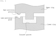
- the step of forming the concave and convex coupling surfaces as the bonding surfaces of the lower ring and the upper ring may be carried out by forming a protrusion protruding from the underside of the upper ring and a concave groove on top of the lower ring in such a manner as to be coupled to the protrusion of the upper ring.
- the concave groove may be symmetrically formed around a central circumferential line on top of the lower ring and has the shape of a circular groove formed over the entire width of top of the lower ring.
- a distance to the deepest portion of the concave groove from top of the lower ring may be 3 to 5 mm, and a length of the deepest portion of the concave groove along the width direction of top of the lower ring may be within 70% of the entire width of top of the lower ring.
- the upper ring may have an upper positioning protrusion protruding from the underside thereof
- the lower ring has a lower positioning groove formed on a given portion of top thereof in such a manner as to be coupled to the upper positioning protrusion of the upper ring, the lower positioning groove being formed between an outer center line between the central circumferential line and an outer circumferential line of the lower ring and the outer circumferential line of the lower ring or being formed between an inner center line between the central circumferential line and an inner circumferential line of the lower ring and the inner circumferential line of the lower ring.
- the lower positioning groove may be a hemispherical groove.
- the lower ring and the upper ring are mounted on a lower ring fixing device made of molybdenum and an upper ring fixing device made of molybdenum in the silicon part fusion bonding apparatus, respectively.
- the step of heating and fusing the bonding surface of the lower ring and the upper ring may include the steps of: forming a vacuum atmosphere of 90 to 110 torr; injecting argon gas to maintain a vacuum level of 50 to 70 torr; applying a given pressure to a space between the lower ring and the upper ring by means of the lower ring fixing device and the upper ring fixing device; operating upper heaters and lower heaters to increase an atmospheric temperature of a vacuum furnace in which a crucible is mounted; operating side heaters capable of performing high-frequency induction heating to locally heat the fusion portion of the bonding surfaces; and cooling the fusion portion.
- a fusing temperature of the fusion portion through the operation of the side heaters capable of performing the high-frequency induction heating is in the range of 1500 to 1600°C.
- the step of cooling the fusion portion is carried out by turning off the side heaters capable of performing the high-frequency induction heating after the fusion portion has been fused and step by step decreasing the temperatures of the upper heaters and the lower heaters to 1400°C, 1200°C, 1000°C, 900°C, 700°C, 500°C, and 300°C, while the temperature by the respective step being maintained for 10 to 20 minutes.
- a silicon part is used in an etching device when a semiconductor is manufactured in a plasma processing chamber, and the silicon part is made of any one material selected from the group consisting of single crystal silicon (mono c-Si), polycrystalline silicon (poly c-Si), sapphire, Y203, SiC, Quartz, Si 3 N 4 , and ZrO 2 .
- the silicon part represents a consumable part such as the C-ring constituting a plasma processing chamber of FIG.1 as disclosed in Korean Utility Model Registration No. 20-0478935 .
- a silicon part fusion bonding apparatus using silicon powder and high-frequency heaters is modifiedly provided as very similar equipment to a silicon ingot manufacturing apparatus for producing a silicon ingot in the same technical field as the present invention, which is disclosed in Korean Patent No. 10-0916843 and Korean Patent Application Laid-open No. 10-2011-0038040 .
- the present invention may utilize the technologies related to heaters, coolers, control of the heaters and the coolers, a structure of fixing a crucible, and the like that are applied to the above-mentioned conventional technologies, but for the brevity of the description, detailed explanations of the technologies will be avoided.
- FIG. 1 a whole configuration of the silicon part fusion bonding apparatus using silicon powder and high-frequency heaters according to the present invention is shown in FIG. 1 .
- a vacuum furnace 10 includes a crucible 80 for ensuring a space in which a silicon part A (corresponding to an upper ring of a C-ring as an exemplary part of FIG. 2 ) and a silicon part B (corresponding to a lower ring of the C-ring as the exemplary part of FIG.
- the water cooled upper heaters 60 using the resistance heating may be configured as resistance heating wires such as carbon resistance heaters, which are buried in the upper ring fixing device 30 that is made of molybdenum and moves up and down to fixedly mount the silicon part A and thus pressurize the silicon part A
- the water cooled lower heaters 70 using the resistance heating may be configured as resistance heating wires such as carbon resistance heaters, which are buried in the lower ring fixing device 20 that is made of molybdenum to fixedly mount the silicon part B.
- a heating device for supplying cooling water, a vacuum maintaining device, a temperature control device, an argon (Ar) atmosphere maintaining and gas introducing and exhausting device, and the like that are used in a silicon ingot manufacturing apparatus or an etching and film deposition apparatus may be additionally provided even though not shown.
- the upper ring of the C-ring as one of the silicon parts is the silicon part A and the lower ring thereof is the silicon part B.
- a part where slits are formed on the C-ring is called the upper ring for the conveniences of the description, but of course, the part may be called the lower ring.
- the method for fusedly bonding silicon parts using silicon powder and high-frequency heaters according to the present invention includes the step of making an upper ring.
- a C-ring as disclosed in Korean Utility Model Registration No. 20-0478935 or a silicon disc cut off through a sawing process as disclosed in Korean Patent No. 10-2102132 is prepared.
- a core drilling (or coring) process is performed to form a silicon ring body on which a through hole is formed on the silicon disc.
- the silicon ring body with the coring process is machined in inner and outer circumferential surfaces by means of a grinding machine or machining center tool (MCT), and additional processes for the silicon ring body are performed by means of a silicon part machining method for forming various holes thereon with an electrical discharge machine.
- MCT machining center tool
- the method for fusedly bonding silicon parts according to the present invention includes the step of making a lower ring.
- the lower ring is made through the method for manufacturing the C-ring as disclosed in Korean Utility Model Registration No. 20-0478935 or the C-ring as disclosed in Korean Patent No. 10-2102132 .
- a silicon disc cut off through a wire sawing process is prepared, and next, a core drilling (or coring) process is performed to form a silicon ring body on which a through hole is formed on the silicon disc.
- the silicon ring body with the coring process is machined in inner and outer circumferential surfaces by means of a grinding machine or MCT, and additional processes for the silicon ring body are performed by means of the silicon part machining method for forming various holes thereon with an electrical discharge machine.
- the method for fusedly bonding silicon parts includes the step of forming concave and convex coupling surfaces as the bonding surfaces of the upper ring and the lower ring.
- silicon powder is filled on top of the lower ring coming into contact with the upper ring, and a concave groove is then formed on top of the lower ring so that it is coupled to a protrusion as will be discussed later formed on the underside of the upper ring.
- the concave groove is symmetrically formed around a central circumferential line (imaginary circumferential line) on top of the lower ring and is a circular groove formed over the entire top of the lower ring.
- a size of the concave groove may change in accordance with the size and material of the C-ring.
- the vertical sectional shape of the lower ring is desirably , but it is limited thereto.
- a distance to the deepest portion of the concave groove from top of the lower ring is 3 to 5 mm, and a length of the deepest portion of the concave groove along the width direction of top of the lower ring is desirably within 70% of the entire width of top of the lower ring.
- a lower positioning groove is formed close to the concave groove to allow the lower ring to be aligned with the upper ring when the lower ring is bonded to the upper ring.
- the upper ring has an upper positioning protrusion protruding from the underside thereof
- the lower ring has the lower positioning groove formed on a portion of top thereof in such a manner as to be coupled to the upper positioning protrusion of the upper ring.
- the lower positioning groove is formed between an outer center line between the central circumferential line and an outer circumferential line of the lower ring and the outer circumferential line of the lower ring, and otherwise, it may be formed between an inner center line between the central circumferential line and an inner circumferential line of the lower ring and the inner circumferential line of the lower ring.
- One or two lower positioning grooves may be formed on the outer or inner side of top of the lower ring from the central circumferential line of top of the lower ring, and the position of the lower positioning groove is desirably at the intermediate point between the central circumferential line and the outer circumferential line of top of the lower ring or at the intermediate point between the central circumferential line and the inner circumferential line of top of the lower ring.
- the lower positioning groove is a hemispherical groove having a maximum protruding height of 1 mm and a maximum diameter of 1 mm.
- the lower positioning groove is machined by means of a grinding machine or MCT, and additional processes for the lower positioning groove are performed by means of electrical discharging or etching.
- the method for fusedly bonding silicon parts according to the present invention includes the step of mounting the lower ring and the upper ring on the silicon part fusion bonding apparatus as shown in FIG. 1 .
- the step of mounting the lower ring and the upper ring is carried out by mounting the lower ring and the upper ring on the lower ring fixing device 20 made of the molybdenum and the upper ring fixing device 30 made of the molybdenum of the silicon part fusion bonding apparatus, respectively.
- each mounting part may have the shape of a simple flat plate corresponding to the shape of each silicon part.
- the method for fusedly bonding silicon parts includes the step of injecting single crystal silicon powder into the concave and convex coupling surfaces as the bonding surfaces of the lower ring and the upper ring, so that the single crystal silicon powder as a melting and bonding agent is fused between the concave and convex coupling surfaces as the bonding surfaces of the lower ring and the upper ring to fusedly bond the lower ring and the upper ring.
- an amount of single crystal silicon powder injected may change in accordance with the sizes of the lower ring and the upper ring, but when the single crystal silicon powder is fused to couple the lower ring and the upper ring to each other, for example, a fusion thickness of the silicon powder is 70%, while a fusion thickness of the bonding surfaces of the upper ring and the lower ring is being 30%, so that a fusion portion of 3 mm is desirably formed, which is appropriate when considering mechanical strength or welded surface machining efficiency to be carried out later.
- the size of the fusion portion may change in accordance with the sizes and material characteristics of the silicon parts and the shapes of the bonding surfaces, and therefore, it may not be limited to the above-mentioned size.
- the method for fusedly bonding silicon parts includes the step of mounting the upper ring and the lower ring on the silicon part fusion bonding apparatus to fusedly bond the upper ring and the lower ring by means of heating and cooling.
- the step is divided into the following sub-steps.
- the upper ring and the lower ring reach a vacuum atmosphere of 90 to 110 torr by means of a vacuum pump of the silicon part fusion bonding apparatus.
- argon (Ar) gas is injected to maintain a vacuum atmosphere of 50 to 70 torr.
- a pressure is applied to a space between the upper ring and the lower ring by means of the upper ring fixing device 30 and the lower ring fixing device 20.
- the application of the pressure is because when the fusion portion is heated by the side heaters 50 capable of performing high-frequency induction heating and is then cooled, the silicon of the fusion portion may be expanded. Through the application of the pressure, therefore, the expansion of the silicon can be suppressed, and of course, the pressure size applied may change in accordance with a product size, especially, a thickness of a welded portion.
- the pressure is 1 kg/cm 2
- the pressure applied is in the range of 0.5 to 5 kg/cm 2 .
- the upper heaters 60 and the lower heaters 70 operate to increase an atmospheric temperature of the vacuum furnace 10 in which the crucible 80 is mounted up to 1300°C.
- the silicon parts may be cracked according to silicon material characteristics, and accordingly, after the upper heaters 60 and the lower heaters 70 as the internal atmospheric temperature heaters (carbon resistance heaters) at the vacuum atmosphere of 90 torr (to which Ar gas is constantly supplied to thus maintain the vacuum level) are raised up to 300°C and then kept at the temperature for 30 minutes. Next, they are step by step raised up to 1180°C and then kept at each raised temperature for 30 minutes.
- the upper heaters 60 and the lower heaters 70 as the internal atmospheric temperature heaters (carbon resistance heaters) at the vacuum atmosphere of 90 torr (to which Ar gas is constantly supplied to thus maintain the vacuum level) are raised up to 300°C and then kept at the temperature for 30 minutes.
- they are step by step raised up to 1180°C and then kept at each raised temperature for 30 minutes.
- the internal atmospheric temperature heaters are raised up to 1420°C to maintain the atmospheric temperature of the vacuum furnace 10 to 1300°C.
- the side heaters 50 capable of performing the high-frequency induction heating operate to locally heat the fusion portion.
- the side heaters 50 capable of performing the high-frequency induction heating operate to heat the fusion portion up to a temperature of 1550°C at which the fusing portion is fused.
- the heating temperature is step by step raised to prevent the thermal shock from occurring.
- the heating temperature may change in accordance with the thicknesses and shapes of the silicon parts, but generally, the heating temperature is desirably in the range of 1500 to 1600°C, more desirably 1550°C.
- the heating temperature is less than 1500°C, the silicon powder is locally fused, thereby failing to bond the lower ring and the upper ring, and contrarily, if the heating temperature is greater than 1600°C, the fusing surface of the silicon parts may collapse.
- the fusion portion is cooled. That is, the fusion portion is formed at the heating temperature of 1550°C, and next, the side heaters 50 capable of performing the high-frequency induction heating is turned off.
- the upper heaters 60 and the lower heaters 70 are controlled to step by step decrease their temperature to the units of 1400°C, 1200°C, 1000°C, 900°C, 700°C, 500°C, 300°C, and 100°C and then maintain the temperature by the respective step for 10 to 20 minutes.
- the upper heaters 60 and the lower heaters 70 are turned off.
- the fusion portion is naturally cooled to a temperature of 100°C or less by means of the Ar gas, thereby finishing the fusion bonding of the silicon parts.
- the method for fusedly bonding the silicon parts to each other includes the steps of forming the concave and convex coupling surfaces on the bonding surfaces of the lower ring and the upper ring, mounting the lower ring and the upper ring on a silicon part fusion bonding apparatus, injecting the single crystal silicon powder into the concave and convex coupling surfaces on the bonding surfaces of the lower ring and the upper ring, and heating and fusing the bonding surfaces of the lower ring and the upper ring, whereby through the simple configuration, qualities of etching and film deposition can be improved.
Landscapes
- Engineering & Computer Science (AREA)
- Chemical & Material Sciences (AREA)
- Mechanical Engineering (AREA)
- Materials Engineering (AREA)
- Crystallography & Structural Chemistry (AREA)
- Metallurgy (AREA)
- Organic Chemistry (AREA)
- Crystals, And After-Treatments Of Crystals (AREA)
- Physics & Mathematics (AREA)
- Optics & Photonics (AREA)
- Ceramic Products (AREA)
- Pressure Welding/Diffusion-Bonding (AREA)
Claims (10)
- Verfahren zum Verbinden von Siliziumteilen unter Verwendung von Siliziumpulver und einer Hochfrequenzheizvorrichtung, das Verfahren umfassend die Schritte:Ausbilden konkaver und konvexer Kopplungsflächen auf den Verbindungsflächen eines unteren Rings und eines oberen Rings,Anbringen des unteren Rings und des oberen Rings auf einer Vorrichtung zum Schmelzschweißen von Siliziumteilen,Einspritzen von einkristallinem Siliziumpulver in die konkaven und konvexen Kopplungsflächen auf den Verbindungsflächen des unteren Rings und des oberen Rings undErhitzen und Verschmelzen der Verbindungsflächen des unteren Rings und des oberen Rings.
- Verfahren nach Anspruch 1, wobei der Schritt des Ausbildens der konkaven und konvexen Kopplungsflächen auf den Verbindungsflächen des unteren Rings und des oberen Rings durch Ausbilden eines Vorsprungs, der von der Unterseite des oberen Rings vorsteht, und einer konkaven Auskehlung auf der Oberseite des unteren Ring derart durchgeführt wird, dass sie mit dem Vorsprung des oberen Rings gekoppelt wird.
- Verfahren nach Anspruch 2, wobei die konkave Auskehlung symmetrisch um eine zentrale Umfangslinie an der Oberseite des unteren Rings ausgebildet ist und die Form einer kreisförmigen Auskehlung aufweist, die über die gesamte Breite der Oberseite des unteren Rings ausgebildet ist.
- Verfahren nach Anspruch 2, wobei der Abstand zum tiefsten Abschnitt der konkaven Auskehlung von der Oberseite des unteren Rings 3 bis 5 mm beträgt und die Länge des tiefsten Abschnitts der konkaven Auskehlung entlang der Breitenrichtung der Oberseite des unteren Rings innerhalb von 70 % der gesamten Breite der Oberkante des unteren Rings beträgt.
- Verfahren nach Anspruch 2, wobei der obere Ring einen oberen Positionierungsvorsprung aufweist, der von der Unterseite davon hervorsteht, und der untere Ring eine untere Positionierungsauskehlung aufweist, die an einem bestimmten Abschnitt seiner Oberseite derart ausgebildet ist, dass sie mit dem oberen Positionierungsvorsprung des oberen Rings gekoppelt wird, wobei die untere Positionierungsauskehlung zwischen einer äußeren Mittellinie zwischen der zentralen Umfangslinie und einer äußeren Umfangslinie des unteren Rings und der äußeren Umfangslinie des unteren Rings ausgebildet ist oder zwischen einer inneren Mittellinie zwischen der zentralen Umfangslinie und einer inneren Umfangslinie des unteren Rings und der inneren Umfangslinie des unteren Rings ausgebildet ist.
- Verfahren nach Anspruch 5, wobei die untere Positionierungsauskehlung eine halbkugelförmige Auskehlung ist.
- Verfahren nach Anspruch 1, wobei nach dem Einfüllen des Siliziumpulvers als Schmelzmittel in einen Schmelzabschnitt zwischen dem unteren Ring und dem oberen Ring der untere Ring und der obere Ring auf einer Befestigungsvorrichtung für den unteren Ring, die aus Molybdän gefertigt ist, bzw. auf einer Befestigungsvorrichtung für den oberen Ring, die aus Molybdän gefertigt ist, in der Vorrichtung zum Schmelzschweißen von Siliziumteilen angebracht werden.
- Verfahren nach Anspruch 1, wobei der Schritt des Erhitzens und Verschmelzens der Verbindungsflächen des unteren Rings und des oberen Rings die folgenden Schritte umfasst:Ausbilden einer Vakuumatmosphäre von 90 bis 110 Torr,Einspritzen von Argongas, um ein Vakuumniveau von 50 bis 70 Torr aufrechtzuerhalten,Ausüben eines vorgegebenen Drucks auf einen Raum zwischen dem unteren Ring und dem oberen Ring mittels der Befestigungsvorrichtung für den unteren Ring und der Befestigungsvorrichtung für den oberen Ring,Betreiben von oberen Heizvorrichtungen und unteren Heizvorrichtungen, um die Atmosphärentemperatur eines Vakuumofens zu erhöhen, in dem ein Tiegel untergebracht ist,Betreiben von seitlichen Heizvorrichtungen, die in der Lage sind, eine Hochfrequenz-Induktionserwärmung auszuführen, um den Schmelzabschnitt der Verbindungsflächen lokal zu erwärmen, undAbkühlen des Schmelzabschnitts.
- Verfahren nach Anspruch 8, wobei eine Schmelztemperatur des Schmelzabschnitts durch den Betrieb der seitlichen Heizvorrichtungen, die in der Lage sind, die Hochfrequenz-Induktionserwärmung auszuführen, im Bereich von 1500 bis 1600 °C liegt.
- Verfahren nach Anspruch 8, wobei der Schritt des Abkühlens des Schmelzabschnitts durch Abschalten der seitlichen Heizvorrichtungen, die in der Lage sind, die Hochfrequenz-Induktionserwärmung auszuführen, nachdem der Schmelzabschnitt geschmolzen wurde, und schrittweises Absenken der Temperaturen der oberen Heizvorrichtungen und der unteren Heizvorrichtungen auf 1400 °C, 1200 °C, 1000 °C, 900 °C, 700 °C, 500 °C und 300 °C, während die Temperatur im jeweiligen Schritt 10 bis 20 Minuten lang aufrechterhalten wird, durchgeführt wird.
Applications Claiming Priority (1)
| Application Number | Priority Date | Filing Date | Title |
|---|---|---|---|
| KR1020210108822A KR102326741B1 (ko) | 2021-08-18 | 2021-08-18 | 실리콘 파우더와 고주파 가열장치를 이용한 실리콘 부품의 접합 방법 |
Publications (2)
| Publication Number | Publication Date |
|---|---|
| EP4137618A1 EP4137618A1 (de) | 2023-02-22 |
| EP4137618B1 true EP4137618B1 (de) | 2023-12-06 |
Family
ID=78716870
Family Applications (1)
| Application Number | Title | Priority Date | Filing Date |
|---|---|---|---|
| EP22180299.4A Active EP4137618B1 (de) | 2021-08-18 | 2022-06-22 | Verfahren zum verbinden von siliziumbauteilen mit siliziumpulver und einer hochfrequenzheizvorrichtung |
Country Status (5)
| Country | Link |
|---|---|
| US (1) | US20230055541A1 (de) |
| EP (1) | EP4137618B1 (de) |
| KR (1) | KR102326741B1 (de) |
| CN (1) | CN115910892B (de) |
| TW (1) | TWI850702B (de) |
Family Cites Families (25)
| Publication number | Priority date | Publication date | Assignee | Title |
|---|---|---|---|---|
| FR2477823A1 (fr) * | 1980-03-04 | 1981-09-11 | Thomson Csf | Procede de fabrication de transducteurs electromecaniques utilisant au moins un film en polymere et dispositif destine a la mise en oeuvre de ce procede |
| US7713379B2 (en) * | 2005-06-20 | 2010-05-11 | Lam Research Corporation | Plasma confinement rings including RF absorbing material for reducing polymer deposition |
| JP2007332022A (ja) * | 2006-06-13 | 2007-12-27 | Young Sang Cho | 多結晶シリコンインゴット製造装置 |
| JP2008251857A (ja) * | 2007-03-30 | 2008-10-16 | Hitachi High-Technologies Corp | プラズマ処理装置 |
| JP2008300425A (ja) * | 2007-05-29 | 2008-12-11 | Union Material Kk | シリコン結晶の接合方法、及びシリコン結晶製品 |
| EP2180031A4 (de) * | 2007-08-01 | 2011-05-25 | Mitsubishi Chem Corp | Phosphor und herstellungsverfahren dafür, kristallines siliciumnitrid und herstellungsverfahren dafür, phosphorhaltige zusammensetzung, lichtemittierendes bauelement mit dem phosphor, bildanzeigevorrichtung und beleuchtungsgerät |
| US20100209082A1 (en) * | 2008-05-30 | 2010-08-19 | Alta Devices, Inc. | Heating lamp system |
| RU2011101453A (ru) | 2008-06-16 | 2012-07-27 | ДжиТи СОЛАР ИНКОРПОРЕЙТЕД (US) | Системы и способы выращивания монокристаллических кремниевых слитков путем направленного отверждения |
| KR100916843B1 (ko) | 2009-01-13 | 2009-09-14 | 김영조 | 고효율 다결정 실리콘 잉곳 제조장치 |
| KR20120031159A (ko) * | 2009-07-03 | 2012-03-30 | 미쓰비시 가가꾸 가부시키가이샤 | 실리콘의 제조 방법, 실리콘 및 태양 전지용 패널 |
| FR2957544B1 (fr) * | 2010-03-16 | 2012-05-11 | Commissariat Energie Atomique | Procede d'assemblage de pieces en materiaux a base de sic par brasage non-reactif avec ajout d'un renfort, compositions de brasure, et joint et assemblage obtenus par ce procede. |
| KR20110113889A (ko) * | 2010-04-12 | 2011-10-19 | 한서에이치케이(주) | 플라즈마 컨파인먼트 향상이 가능한 펌핑수단을 가지는 플라즈마 에칭장치 |
| KR101064207B1 (ko) * | 2010-06-10 | 2011-09-14 | 엘지이노텍 주식회사 | 고순도 탄화규소 웨이퍼 캐리어 및 그 제조 방법 |
| US8826855B2 (en) | 2010-06-30 | 2014-09-09 | Lam Research Corporation | C-shaped confinement ring for a plasma processing chamber |
| TWI606512B (zh) * | 2012-12-27 | 2017-11-21 | 三菱綜合材料股份有限公司 | 電漿蝕刻裝置用矽構件及電漿蝕刻裝置用矽構件之製造方法 |
| JP5615454B1 (ja) * | 2014-02-25 | 2014-10-29 | コバレントマテリアル株式会社 | フォーカスリング |
| KR101608585B1 (ko) * | 2014-06-27 | 2016-04-04 | 오씨아이 주식회사 | 실리콘 나노파우더를 이용한 폴리실리콘 필라멘트 제조방법 |
| US10475627B2 (en) * | 2016-03-25 | 2019-11-12 | Lam Research Corporation | Carrier ring wall for reduction of back-diffusion of reactive species and suppression of local parasitic plasma ignition |
| JP6146841B1 (ja) * | 2016-08-04 | 2017-06-14 | 日本新工芯技株式会社 | リング状電極 |
| JP6727069B2 (ja) * | 2016-08-09 | 2020-07-22 | 東京エレクトロン株式会社 | 接合装置および接合システム |
| KR200491165Y1 (ko) | 2017-04-14 | 2020-05-15 | 주식회사 월덱스 | 플라즈마 에칭장치용 이체형 한정 링 |
| JP6270191B1 (ja) * | 2017-05-17 | 2018-01-31 | 日本新工芯技株式会社 | 保護材用リング |
| JP6278498B1 (ja) * | 2017-05-19 | 2018-02-14 | 日本新工芯技株式会社 | リング状部材の製造方法及びリング状部材 |
| KR102040281B1 (ko) * | 2018-04-26 | 2019-11-04 | 주식회사 건테크 | CVD-SiC 소재를 이용한 반도체 플라즈마 에칭 공정용 한정 링 |
| KR102102132B1 (ko) | 2019-07-03 | 2020-04-20 | 주식회사 테크놀로지메이컬스 | 반도체 식각장치의 결합형 실리콘 링 |
-
2021
- 2021-08-18 KR KR1020210108822A patent/KR102326741B1/ko active Active
-
2022
- 2022-06-22 EP EP22180299.4A patent/EP4137618B1/de active Active
- 2022-07-06 US US17/858,283 patent/US20230055541A1/en active Pending
- 2022-07-14 CN CN202210834062.7A patent/CN115910892B/zh active Active
- 2022-07-14 TW TW111126485A patent/TWI850702B/zh active
Also Published As
| Publication number | Publication date |
|---|---|
| CN115910892A (zh) | 2023-04-04 |
| TWI850702B (zh) | 2024-08-01 |
| EP4137618A1 (de) | 2023-02-22 |
| CN115910892B (zh) | 2026-04-17 |
| US20230055541A1 (en) | 2023-02-23 |
| TW202320944A (zh) | 2023-06-01 |
| KR102326741B1 (ko) | 2021-11-16 |
Similar Documents
| Publication | Publication Date | Title |
|---|---|---|
| EP0863545A2 (de) | Elektrostatischer Scheibenhalter aus einkristalliger Keramik | |
| US6581275B2 (en) | Fabricating an electrostatic chuck having plasma resistant gas conduits | |
| JP3129419U (ja) | 基板の温度を制御する装置 | |
| EP1656697B1 (de) | Auf mems basierende mehrpolare elektrostatische einspannvorrichtung | |
| US6946403B2 (en) | Method of making a MEMS electrostatic chuck | |
| KR101582785B1 (ko) | 정전 척 조립체 | |
| US7436645B2 (en) | Method and apparatus for controlling temperature of a substrate | |
| US6572814B2 (en) | Method of fabricating a semiconductor wafer support chuck apparatus having small diameter gas distribution ports for distributing a heat transfer gas | |
| US6639783B1 (en) | Multi-layer ceramic electrostatic chuck with integrated channel | |
| US20050079737A1 (en) | Mems based contact conductivity electrostatic chuck | |
| US6583980B1 (en) | Substrate support tolerant to thermal expansion stresses | |
| US11430686B2 (en) | Pedestal heater for spatial multi-wafer processing tool | |
| KR102864030B1 (ko) | 세라믹 전극 플레이트를 갖는 플라즈마 소스 | |
| JP4418484B2 (ja) | 静電チャック及びそれを用いたワークの冷却方法 | |
| EP4137618B1 (de) | Verfahren zum verbinden von siliziumbauteilen mit siliziumpulver und einer hochfrequenzheizvorrichtung | |
| JP2023546087A (ja) | 半導体基板支持体電力伝達部品 | |
| TWI922523B (zh) | 具有陶瓷電極板的電漿源及處理基板之方法 | |
| US20240387154A1 (en) | Afe (active far edge) heater/bipolar esc with simplified and optimized structure for greater reliability, lower cost and better manufacturability | |
| JP3976994B2 (ja) | シリコンヒータ | |
| JP2025016070A (ja) | シャフト付セラミックスヒータ | |
| JP2025526053A (ja) | 静電チャック用真空シール | |
| CN119301731A (zh) | 通过电子束熔化而焊接的硅部件 | |
| CN104752118A (zh) | 等离子体处理腔室及其静电夹盘的制造方法 |
Legal Events
| Date | Code | Title | Description |
|---|---|---|---|
| PUAI | Public reference made under article 153(3) epc to a published international application that has entered the european phase |
Free format text: ORIGINAL CODE: 0009012 |
|
| STAA | Information on the status of an ep patent application or granted ep patent |
Free format text: STATUS: REQUEST FOR EXAMINATION WAS MADE |
|
| 17P | Request for examination filed |
Effective date: 20220622 |
|
| AK | Designated contracting states |
Kind code of ref document: A1 Designated state(s): AL AT BE BG CH CY CZ DE DK EE ES FI FR GB GR HR HU IE IS IT LI LT LU LV MC MK MT NL NO PL PT RO RS SE SI SK SM TR |
|
| REG | Reference to a national code |
Ref legal event code: R079 Free format text: PREVIOUS MAIN CLASS: C30B0029060000 Ref country code: DE Ref legal event code: R079 Ref document number: 602022001222 Country of ref document: DE Free format text: PREVIOUS MAIN CLASS: C30B0029060000 Ipc: B23K0001060000 |
|
| GRAP | Despatch of communication of intention to grant a patent |
Free format text: ORIGINAL CODE: EPIDOSNIGR1 |
|
| STAA | Information on the status of an ep patent application or granted ep patent |
Free format text: STATUS: GRANT OF PATENT IS INTENDED |
|
| RIC1 | Information provided on ipc code assigned before grant |
Ipc: B23K 1/19 20060101ALI20230721BHEP Ipc: C30B 33/06 20060101ALI20230721BHEP Ipc: C30B 29/06 20060101ALI20230721BHEP Ipc: B23K 1/06 20060101AFI20230721BHEP |
|
| INTG | Intention to grant announced |
Effective date: 20230823 |
|
| GRAS | Grant fee paid |
Free format text: ORIGINAL CODE: EPIDOSNIGR3 |
|
| GRAA | (expected) grant |
Free format text: ORIGINAL CODE: 0009210 |
|
| STAA | Information on the status of an ep patent application or granted ep patent |
Free format text: STATUS: THE PATENT HAS BEEN GRANTED |
|
| AK | Designated contracting states |
Kind code of ref document: B1 Designated state(s): AL AT BE BG CH CY CZ DE DK EE ES FI FR GB GR HR HU IE IS IT LI LT LU LV MC MK MT NL NO PL PT RO RS SE SI SK SM TR |
|
| REG | Reference to a national code |
Ref country code: GB Ref legal event code: FG4D |
|
| REG | Reference to a national code |
Ref country code: DE Ref legal event code: R096 Ref document number: 602022001222 Country of ref document: DE |
|
| REG | Reference to a national code |
Ref country code: CH Ref legal event code: EP |
|
| REG | Reference to a national code |
Ref country code: IE Ref legal event code: FG4D |
|
| REG | Reference to a national code |
Ref country code: LT Ref legal event code: MG9D |
|
| PG25 | Lapsed in a contracting state [announced via postgrant information from national office to epo] |
Ref country code: GR Free format text: LAPSE BECAUSE OF FAILURE TO SUBMIT A TRANSLATION OF THE DESCRIPTION OR TO PAY THE FEE WITHIN THE PRESCRIBED TIME-LIMIT Effective date: 20240307 |
|
| REG | Reference to a national code |
Ref country code: NL Ref legal event code: MP Effective date: 20231206 |
|
| PG25 | Lapsed in a contracting state [announced via postgrant information from national office to epo] |
Ref country code: LT Free format text: LAPSE BECAUSE OF FAILURE TO SUBMIT A TRANSLATION OF THE DESCRIPTION OR TO PAY THE FEE WITHIN THE PRESCRIBED TIME-LIMIT Effective date: 20231206 |
|
| PG25 | Lapsed in a contracting state [announced via postgrant information from national office to epo] |
Ref country code: ES Free format text: LAPSE BECAUSE OF FAILURE TO SUBMIT A TRANSLATION OF THE DESCRIPTION OR TO PAY THE FEE WITHIN THE PRESCRIBED TIME-LIMIT Effective date: 20231206 |
|
| PG25 | Lapsed in a contracting state [announced via postgrant information from national office to epo] |
Ref country code: LT Free format text: LAPSE BECAUSE OF FAILURE TO SUBMIT A TRANSLATION OF THE DESCRIPTION OR TO PAY THE FEE WITHIN THE PRESCRIBED TIME-LIMIT Effective date: 20231206 Ref country code: GR Free format text: LAPSE BECAUSE OF FAILURE TO SUBMIT A TRANSLATION OF THE DESCRIPTION OR TO PAY THE FEE WITHIN THE PRESCRIBED TIME-LIMIT Effective date: 20240307 Ref country code: ES Free format text: LAPSE BECAUSE OF FAILURE TO SUBMIT A TRANSLATION OF THE DESCRIPTION OR TO PAY THE FEE WITHIN THE PRESCRIBED TIME-LIMIT Effective date: 20231206 Ref country code: BG Free format text: LAPSE BECAUSE OF FAILURE TO SUBMIT A TRANSLATION OF THE DESCRIPTION OR TO PAY THE FEE WITHIN THE PRESCRIBED TIME-LIMIT Effective date: 20240306 |
|
| REG | Reference to a national code |
Ref country code: AT Ref legal event code: MK05 Ref document number: 1637938 Country of ref document: AT Kind code of ref document: T Effective date: 20231206 |
|
| PG25 | Lapsed in a contracting state [announced via postgrant information from national office to epo] |
Ref country code: NL Free format text: LAPSE BECAUSE OF FAILURE TO SUBMIT A TRANSLATION OF THE DESCRIPTION OR TO PAY THE FEE WITHIN THE PRESCRIBED TIME-LIMIT Effective date: 20231206 |
|
| PG25 | Lapsed in a contracting state [announced via postgrant information from national office to epo] |
Ref country code: SE Free format text: LAPSE BECAUSE OF FAILURE TO SUBMIT A TRANSLATION OF THE DESCRIPTION OR TO PAY THE FEE WITHIN THE PRESCRIBED TIME-LIMIT Effective date: 20231206 Ref country code: RS Free format text: LAPSE BECAUSE OF FAILURE TO SUBMIT A TRANSLATION OF THE DESCRIPTION OR TO PAY THE FEE WITHIN THE PRESCRIBED TIME-LIMIT Effective date: 20231206 Ref country code: NO Free format text: LAPSE BECAUSE OF FAILURE TO SUBMIT A TRANSLATION OF THE DESCRIPTION OR TO PAY THE FEE WITHIN THE PRESCRIBED TIME-LIMIT Effective date: 20240306 Ref country code: NL Free format text: LAPSE BECAUSE OF FAILURE TO SUBMIT A TRANSLATION OF THE DESCRIPTION OR TO PAY THE FEE WITHIN THE PRESCRIBED TIME-LIMIT Effective date: 20231206 Ref country code: LV Free format text: LAPSE BECAUSE OF FAILURE TO SUBMIT A TRANSLATION OF THE DESCRIPTION OR TO PAY THE FEE WITHIN THE PRESCRIBED TIME-LIMIT Effective date: 20231206 Ref country code: HR Free format text: LAPSE BECAUSE OF FAILURE TO SUBMIT A TRANSLATION OF THE DESCRIPTION OR TO PAY THE FEE WITHIN THE PRESCRIBED TIME-LIMIT Effective date: 20231206 |
|
| PG25 | Lapsed in a contracting state [announced via postgrant information from national office to epo] |
Ref country code: IS Free format text: LAPSE BECAUSE OF FAILURE TO SUBMIT A TRANSLATION OF THE DESCRIPTION OR TO PAY THE FEE WITHIN THE PRESCRIBED TIME-LIMIT Effective date: 20240406 |
|
| PG25 | Lapsed in a contracting state [announced via postgrant information from national office to epo] |
Ref country code: CZ Free format text: LAPSE BECAUSE OF FAILURE TO SUBMIT A TRANSLATION OF THE DESCRIPTION OR TO PAY THE FEE WITHIN THE PRESCRIBED TIME-LIMIT Effective date: 20231206 Ref country code: AT Free format text: LAPSE BECAUSE OF FAILURE TO SUBMIT A TRANSLATION OF THE DESCRIPTION OR TO PAY THE FEE WITHIN THE PRESCRIBED TIME-LIMIT Effective date: 20231206 |
|
| PG25 | Lapsed in a contracting state [announced via postgrant information from national office to epo] |
Ref country code: SK Free format text: LAPSE BECAUSE OF FAILURE TO SUBMIT A TRANSLATION OF THE DESCRIPTION OR TO PAY THE FEE WITHIN THE PRESCRIBED TIME-LIMIT Effective date: 20231206 |
|
| PG25 | Lapsed in a contracting state [announced via postgrant information from national office to epo] |
Ref country code: SM Free format text: LAPSE BECAUSE OF FAILURE TO SUBMIT A TRANSLATION OF THE DESCRIPTION OR TO PAY THE FEE WITHIN THE PRESCRIBED TIME-LIMIT Effective date: 20231206 Ref country code: SK Free format text: LAPSE BECAUSE OF FAILURE TO SUBMIT A TRANSLATION OF THE DESCRIPTION OR TO PAY THE FEE WITHIN THE PRESCRIBED TIME-LIMIT Effective date: 20231206 Ref country code: RO Free format text: LAPSE BECAUSE OF FAILURE TO SUBMIT A TRANSLATION OF THE DESCRIPTION OR TO PAY THE FEE WITHIN THE PRESCRIBED TIME-LIMIT Effective date: 20231206 Ref country code: IT Free format text: LAPSE BECAUSE OF FAILURE TO SUBMIT A TRANSLATION OF THE DESCRIPTION OR TO PAY THE FEE WITHIN THE PRESCRIBED TIME-LIMIT Effective date: 20231206 Ref country code: IS Free format text: LAPSE BECAUSE OF FAILURE TO SUBMIT A TRANSLATION OF THE DESCRIPTION OR TO PAY THE FEE WITHIN THE PRESCRIBED TIME-LIMIT Effective date: 20240406 Ref country code: EE Free format text: LAPSE BECAUSE OF FAILURE TO SUBMIT A TRANSLATION OF THE DESCRIPTION OR TO PAY THE FEE WITHIN THE PRESCRIBED TIME-LIMIT Effective date: 20231206 Ref country code: CZ Free format text: LAPSE BECAUSE OF FAILURE TO SUBMIT A TRANSLATION OF THE DESCRIPTION OR TO PAY THE FEE WITHIN THE PRESCRIBED TIME-LIMIT Effective date: 20231206 Ref country code: AT Free format text: LAPSE BECAUSE OF FAILURE TO SUBMIT A TRANSLATION OF THE DESCRIPTION OR TO PAY THE FEE WITHIN THE PRESCRIBED TIME-LIMIT Effective date: 20231206 |
|
| PG25 | Lapsed in a contracting state [announced via postgrant information from national office to epo] |
Ref country code: PT Free format text: LAPSE BECAUSE OF FAILURE TO SUBMIT A TRANSLATION OF THE DESCRIPTION OR TO PAY THE FEE WITHIN THE PRESCRIBED TIME-LIMIT Effective date: 20240408 Ref country code: PL Free format text: LAPSE BECAUSE OF FAILURE TO SUBMIT A TRANSLATION OF THE DESCRIPTION OR TO PAY THE FEE WITHIN THE PRESCRIBED TIME-LIMIT Effective date: 20231206 |
|
| REG | Reference to a national code |
Ref country code: DE Ref legal event code: R097 Ref document number: 602022001222 Country of ref document: DE |
|
| PG25 | Lapsed in a contracting state [announced via postgrant information from national office to epo] |
Ref country code: DK Free format text: LAPSE BECAUSE OF FAILURE TO SUBMIT A TRANSLATION OF THE DESCRIPTION OR TO PAY THE FEE WITHIN THE PRESCRIBED TIME-LIMIT Effective date: 20231206 |
|
| PLBE | No opposition filed within time limit |
Free format text: ORIGINAL CODE: 0009261 |
|
| STAA | Information on the status of an ep patent application or granted ep patent |
Free format text: STATUS: NO OPPOSITION FILED WITHIN TIME LIMIT |
|
| PG25 | Lapsed in a contracting state [announced via postgrant information from national office to epo] |
Ref country code: SI Free format text: LAPSE BECAUSE OF FAILURE TO SUBMIT A TRANSLATION OF THE DESCRIPTION OR TO PAY THE FEE WITHIN THE PRESCRIBED TIME-LIMIT Effective date: 20231206 |
|
| PG25 | Lapsed in a contracting state [announced via postgrant information from national office to epo] |
Ref country code: SI Free format text: LAPSE BECAUSE OF FAILURE TO SUBMIT A TRANSLATION OF THE DESCRIPTION OR TO PAY THE FEE WITHIN THE PRESCRIBED TIME-LIMIT Effective date: 20231206 Ref country code: DK Free format text: LAPSE BECAUSE OF FAILURE TO SUBMIT A TRANSLATION OF THE DESCRIPTION OR TO PAY THE FEE WITHIN THE PRESCRIBED TIME-LIMIT Effective date: 20231206 |
|
| 26N | No opposition filed |
Effective date: 20240909 |
|
| REG | Reference to a national code |
Ref country code: DE Ref legal event code: R119 Ref document number: 602022001222 Country of ref document: DE |
|
| PG25 | Lapsed in a contracting state [announced via postgrant information from national office to epo] |
Ref country code: MC Free format text: LAPSE BECAUSE OF FAILURE TO SUBMIT A TRANSLATION OF THE DESCRIPTION OR TO PAY THE FEE WITHIN THE PRESCRIBED TIME-LIMIT Effective date: 20231206 |
|
| PG25 | Lapsed in a contracting state [announced via postgrant information from national office to epo] |
Ref country code: LU Free format text: LAPSE BECAUSE OF NON-PAYMENT OF DUE FEES Effective date: 20240622 |
|
| PG25 | Lapsed in a contracting state [announced via postgrant information from national office to epo] |
Ref country code: DE Free format text: LAPSE BECAUSE OF NON-PAYMENT OF DUE FEES Effective date: 20250101 |
|
| PG25 | Lapsed in a contracting state [announced via postgrant information from national office to epo] |
Ref country code: IE Free format text: LAPSE BECAUSE OF NON-PAYMENT OF DUE FEES Effective date: 20240622 |
|
| PG25 | Lapsed in a contracting state [announced via postgrant information from national office to epo] |
Ref country code: BE Free format text: LAPSE BECAUSE OF NON-PAYMENT OF DUE FEES Effective date: 20240630 |
|
| PG25 | Lapsed in a contracting state [announced via postgrant information from national office to epo] |
Ref country code: FR Free format text: LAPSE BECAUSE OF NON-PAYMENT OF DUE FEES Effective date: 20240630 |
|
| REG | Reference to a national code |
Ref country code: BE Ref legal event code: MM Effective date: 20240630 |
|
| PG25 | Lapsed in a contracting state [announced via postgrant information from national office to epo] |
Ref country code: FI Free format text: LAPSE BECAUSE OF FAILURE TO SUBMIT A TRANSLATION OF THE DESCRIPTION OR TO PAY THE FEE WITHIN THE PRESCRIBED TIME-LIMIT Effective date: 20231207 |
|
| PG25 | Lapsed in a contracting state [announced via postgrant information from national office to epo] |
Ref country code: CY Free format text: LAPSE BECAUSE OF FAILURE TO SUBMIT A TRANSLATION OF THE DESCRIPTION OR TO PAY THE FEE WITHIN THE PRESCRIBED TIME-LIMIT; INVALID AB INITIO Effective date: 20220622 |
|
| REG | Reference to a national code |
Ref country code: CH Ref legal event code: H13 Free format text: ST27 STATUS EVENT CODE: U-0-0-H10-H13 (AS PROVIDED BY THE NATIONAL OFFICE) Effective date: 20260127 |
|
| PG25 | Lapsed in a contracting state [announced via postgrant information from national office to epo] |
Ref country code: HU Free format text: LAPSE BECAUSE OF FAILURE TO SUBMIT A TRANSLATION OF THE DESCRIPTION OR TO PAY THE FEE WITHIN THE PRESCRIBED TIME-LIMIT; INVALID AB INITIO Effective date: 20220622 |
|
| PG25 | Lapsed in a contracting state [announced via postgrant information from national office to epo] |
Ref country code: CH Free format text: LAPSE BECAUSE OF NON-PAYMENT OF DUE FEES Effective date: 20250630 |