EP4137623A1 - Procédé de fabrication d'un substrat de nitrure d'aluminium, substrat de nitrure d'aluminium et procédé de formation d'une couche de nitrure d'aluminium - Google Patents
Procédé de fabrication d'un substrat de nitrure d'aluminium, substrat de nitrure d'aluminium et procédé de formation d'une couche de nitrure d'aluminium Download PDFInfo
- Publication number
- EP4137623A1 EP4137623A1 EP21789219.9A EP21789219A EP4137623A1 EP 4137623 A1 EP4137623 A1 EP 4137623A1 EP 21789219 A EP21789219 A EP 21789219A EP 4137623 A1 EP4137623 A1 EP 4137623A1
- Authority
- EP
- European Patent Office
- Prior art keywords
- underlying substrate
- aluminum nitride
- substrate
- sic
- silicon carbide
- Prior art date
- Legal status (The legal status is an assumption and is not a legal conclusion. Google has not performed a legal analysis and makes no representation as to the accuracy of the status listed.)
- Pending
Links
Images


Classifications
-
- C—CHEMISTRY; METALLURGY
- C30—CRYSTAL GROWTH
- C30B—SINGLE-CRYSTAL GROWTH; UNIDIRECTIONAL SOLIDIFICATION OF EUTECTIC MATERIAL OR UNIDIRECTIONAL DEMIXING OF EUTECTOID MATERIAL; REFINING BY ZONE-MELTING OF MATERIAL; PRODUCTION OF A HOMOGENEOUS POLYCRYSTALLINE MATERIAL WITH DEFINED STRUCTURE; SINGLE CRYSTALS OR HOMOGENEOUS POLYCRYSTALLINE MATERIAL WITH DEFINED STRUCTURE; AFTER-TREATMENT OF SINGLE CRYSTALS OR A HOMOGENEOUS POLYCRYSTALLINE MATERIAL WITH DEFINED STRUCTURE; APPARATUS THEREFOR
- C30B23/00—Single-crystal growth by condensing evaporated or sublimed materials
- C30B23/02—Epitaxial-layer growth
- C30B23/025—Epitaxial-layer growth characterised by the substrate
-
- C—CHEMISTRY; METALLURGY
- C30—CRYSTAL GROWTH
- C30B—SINGLE-CRYSTAL GROWTH; UNIDIRECTIONAL SOLIDIFICATION OF EUTECTIC MATERIAL OR UNIDIRECTIONAL DEMIXING OF EUTECTOID MATERIAL; REFINING BY ZONE-MELTING OF MATERIAL; PRODUCTION OF A HOMOGENEOUS POLYCRYSTALLINE MATERIAL WITH DEFINED STRUCTURE; SINGLE CRYSTALS OR HOMOGENEOUS POLYCRYSTALLINE MATERIAL WITH DEFINED STRUCTURE; AFTER-TREATMENT OF SINGLE CRYSTALS OR A HOMOGENEOUS POLYCRYSTALLINE MATERIAL WITH DEFINED STRUCTURE; APPARATUS THEREFOR
- C30B23/00—Single-crystal growth by condensing evaporated or sublimed materials
- C30B23/02—Epitaxial-layer growth
- C30B23/06—Heating of the deposition chamber, the substrate or the materials to be evaporated
- C30B23/063—Heating of the substrate
-
- C—CHEMISTRY; METALLURGY
- C30—CRYSTAL GROWTH
- C30B—SINGLE-CRYSTAL GROWTH; UNIDIRECTIONAL SOLIDIFICATION OF EUTECTIC MATERIAL OR UNIDIRECTIONAL DEMIXING OF EUTECTOID MATERIAL; REFINING BY ZONE-MELTING OF MATERIAL; PRODUCTION OF A HOMOGENEOUS POLYCRYSTALLINE MATERIAL WITH DEFINED STRUCTURE; SINGLE CRYSTALS OR HOMOGENEOUS POLYCRYSTALLINE MATERIAL WITH DEFINED STRUCTURE; AFTER-TREATMENT OF SINGLE CRYSTALS OR A HOMOGENEOUS POLYCRYSTALLINE MATERIAL WITH DEFINED STRUCTURE; APPARATUS THEREFOR
- C30B25/00—Single-crystal growth by chemical reaction of reactive gases, e.g. chemical vapour-deposition growth
- C30B25/02—Epitaxial-layer growth
- C30B25/18—Epitaxial-layer growth characterised by the substrate
- C30B25/186—Epitaxial-layer growth characterised by the substrate being specially pre-treated by, e.g. chemical or physical means
-
- C—CHEMISTRY; METALLURGY
- C30—CRYSTAL GROWTH
- C30B—SINGLE-CRYSTAL GROWTH; UNIDIRECTIONAL SOLIDIFICATION OF EUTECTIC MATERIAL OR UNIDIRECTIONAL DEMIXING OF EUTECTOID MATERIAL; REFINING BY ZONE-MELTING OF MATERIAL; PRODUCTION OF A HOMOGENEOUS POLYCRYSTALLINE MATERIAL WITH DEFINED STRUCTURE; SINGLE CRYSTALS OR HOMOGENEOUS POLYCRYSTALLINE MATERIAL WITH DEFINED STRUCTURE; AFTER-TREATMENT OF SINGLE CRYSTALS OR A HOMOGENEOUS POLYCRYSTALLINE MATERIAL WITH DEFINED STRUCTURE; APPARATUS THEREFOR
- C30B29/00—Single crystals or homogeneous polycrystalline material with defined structure characterised by the material or by their shape
- C30B29/10—Inorganic compounds or compositions
- C30B29/40—AIIIBV compounds wherein A is B, Al, Ga, In or Tl and B is N, P, As, Sb or Bi
- C30B29/403—AIII-nitrides
-
- C—CHEMISTRY; METALLURGY
- C30—CRYSTAL GROWTH
- C30B—SINGLE-CRYSTAL GROWTH; UNIDIRECTIONAL SOLIDIFICATION OF EUTECTIC MATERIAL OR UNIDIRECTIONAL DEMIXING OF EUTECTOID MATERIAL; REFINING BY ZONE-MELTING OF MATERIAL; PRODUCTION OF A HOMOGENEOUS POLYCRYSTALLINE MATERIAL WITH DEFINED STRUCTURE; SINGLE CRYSTALS OR HOMOGENEOUS POLYCRYSTALLINE MATERIAL WITH DEFINED STRUCTURE; AFTER-TREATMENT OF SINGLE CRYSTALS OR A HOMOGENEOUS POLYCRYSTALLINE MATERIAL WITH DEFINED STRUCTURE; APPARATUS THEREFOR
- C30B33/00—After-treatment of single crystals or homogeneous polycrystalline material with defined structure
- C30B33/08—Etching
-
- H—ELECTRICITY
- H10—SEMICONDUCTOR DEVICES; ELECTRIC SOLID-STATE DEVICES NOT OTHERWISE PROVIDED FOR
- H10P—GENERIC PROCESSES OR APPARATUS FOR THE MANUFACTURE OR TREATMENT OF DEVICES COVERED BY CLASS H10
- H10P14/00—Formation of materials, e.g. in the shape of layers or pillars
- H10P14/20—Formation of materials, e.g. in the shape of layers or pillars of semiconductor materials
- H10P14/29—Formation of materials, e.g. in the shape of layers or pillars of semiconductor materials characterised by the substrates
- H10P14/2901—Materials
- H10P14/2902—Materials being Group IVA materials
- H10P14/2904—Silicon carbide
-
- H—ELECTRICITY
- H10—SEMICONDUCTOR DEVICES; ELECTRIC SOLID-STATE DEVICES NOT OTHERWISE PROVIDED FOR
- H10P—GENERIC PROCESSES OR APPARATUS FOR THE MANUFACTURE OR TREATMENT OF DEVICES COVERED BY CLASS H10
- H10P14/00—Formation of materials, e.g. in the shape of layers or pillars
- H10P14/20—Formation of materials, e.g. in the shape of layers or pillars of semiconductor materials
- H10P14/29—Formation of materials, e.g. in the shape of layers or pillars of semiconductor materials characterised by the substrates
- H10P14/2924—Structures
- H10P14/2925—Surface structures
-
- H—ELECTRICITY
- H10—SEMICONDUCTOR DEVICES; ELECTRIC SOLID-STATE DEVICES NOT OTHERWISE PROVIDED FOR
- H10P—GENERIC PROCESSES OR APPARATUS FOR THE MANUFACTURE OR TREATMENT OF DEVICES COVERED BY CLASS H10
- H10P14/00—Formation of materials, e.g. in the shape of layers or pillars
- H10P14/20—Formation of materials, e.g. in the shape of layers or pillars of semiconductor materials
- H10P14/34—Deposited materials, e.g. layers
- H10P14/3402—Deposited materials, e.g. layers characterised by the chemical composition
- H10P14/3414—Deposited materials, e.g. layers characterised by the chemical composition being group IIIA-VIA materials
- H10P14/3416—Nitrides
Definitions
- the present invention relates to a method for manufacturing an aluminum nitride substrate, an aluminum nitride substrate, and a method for forming an aluminum nitride layer.
- a semiconductor substrate is manufactured by crystal-growing a growth layer on an underlying substrate.
- a problem has been reported that it is difficult to obtain a semiconductor substrate having a large diameter depending on compositions of the semiconductor material to be crystal-grown.
- Examples thereof include a case where AlN crystals are grown on an underlying substrate such as an aluminum nitride (AlN) substrate or a silicon carbide (SiC) substrate via a sublimation method.
- AlN aluminum nitride
- SiC silicon carbide
- Patent Literature 1 describes a technique of "a method for growing AlN crystals on a seed crystal substrate arranged in a crystal growth chamber in a crystal growth vessel provided in a reaction vessel via a vapor phase growth method, the method characterized in supplying a carbon-containing gas into the crystal growth chamber during crystal growth".
- Patent Literature 1 JP 2007-55881 A
- An object of the present invention is to provide a novel technique capable of manufacturing a large-diameter AlN substrate.
- Another object of the present invention is to provide a novel technique capable of manufacturing an AlN substrate having a large diameter and excellent crystallinity.
- the present invention that is intended to solve the problems described above is a method for manufacturing an aluminum nitride substrate, including a crystal growth step of forming an aluminum nitride layer on a silicon carbide underlying substrate having through holes.
- an aluminum nitride substrate having a diameter equivalent to the diameter of the silicon carbide underlying substrate can be manufactured. Therefore, by adopting a silicon carbide underlying substrate having a large diameter, an aluminum nitride substrate having a large diameter can be obtained.
- the term "large diameter" in the present description means that an aluminum nitride layer having a large area can be obtained as compared with a case where an aluminum nitride layer is formed on a silicon carbide underlying substrate having no through holes.
- the crystal growth step is a step of heating such that a temperature gradient is formed along a vertical direction of the silicon carbide underlying substrate.
- the crystal growth step is a step in which the silicon carbide underlying substrate and the source of the aluminum nitride layer are disposed in such a way to face each other, and heating is performed such that the temperature gradient is formed between the silicon carbide underlying substrate and the source.
- the crystal growth step includes a lateral growth step of growing the aluminum nitride layer in a horizontal direction of the silicon carbide underlying substrate, and a longitudinal growth step of growing the aluminum nitride layer in a vertical direction of the silicon carbide underlying substrate.
- a through hole formation step of forming through holes in the silicon carbide underlying substrate, and a strained layer removal step of removing a strained layer introduced in the through hole formation step are further included.
- the through hole formation step is a step of forming the through holes by irradiating the silicon carbide underlying substrate with a laser.
- the strained layer removal step is a step of removing a strained layer of the silicon carbide underlying substrate by heat treatment.
- the strained layer removal step is a step of etching the silicon carbide underlying substrate under a silicon atmosphere.
- the present invention also relates to a method for forming an aluminum nitride layer.
- the present invention for solving the problems described above is a method for forming an aluminum nitride layer including the through hole formation step of forming the through holes in the silicon carbide underlying substrate before forming the aluminum nitride layer on the silicon carbide underlying substrate.
- the strained layer removal step of removing a strained layer introduced in the through hole formation step is included.
- the strained layer removal step is a step of etching the silicon carbide underlying substrate by heat treatment.
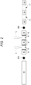
- Figs. 1 to 4 are explanatory views for explaining steps of the method for manufacturing an AlN substrate according to the embodiment of the present invention.
- the method for manufacturing the AlN substrate according to the embodiment may include a through hole formation step S10 of forming through holes 11 in a SiC underlying substrate 10, a strained layer removal step S20 of removing a strained layer 12 introduced in the through hole formation step S10, and a crystal growth step S30 of forming an AlN layer 20 on the SiC underlying substrate 10 having the through holes 11.
- this embodiment can be understood as a method of forming the AlN layer in a large area including the through hole formation step S10 of forming the through holes 11 in the SiC underlying substrate 10 before forming the AlN layer 20 on the surface of the SiC underlying substrate 10.
- the through hole formation step S10 is a step of forming the through holes 11 in the SiC underlying substrate 10.
- the through hole formation step S10 can be naturally adopted as long as it is a method capable of forming the through holes 11 in the SiC underlying substrate 10.
- a plasma etching such as a laser processing, a focused ion beam system (FIB), and a reactive ion etching (RIE) can be adopted as an example.
- FIB focused ion beam system
- RIE reactive ion etching
- SiC underlying substrate 10 a wafer or a substrate processed from a bulk crystal may be used, or a substrate having a buffer layer made of the semiconductor material described above may be separately used.
- a shape that reduces the strength of the SiC underlying substrate 10 may be adopted for the through holes 11, and one or a plurality of through holes may be formed.
- a through hole group (pattern) in which a plurality of through holes 11 are arranged may be adopted.
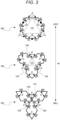
- Fig. 3 is an explanatory view for explaining a pattern 100 according to the embodiment.
- a line segment indicated by the pattern 100 is the SiC underlying substrate 10.
- the pattern 100 preferably presents a regular hexagonal displacement shape that is three-fold symmetric.
- the "regular hexagonal displacement shape" in the description of the present description will be described in detail below with reference to Fig. 3 .
- the regular hexagonal displacement shape is a 12 polygon.
- the regular hexagonal displacement shape is constituted by 12 straight line segments having the same length.
- the pattern 100 having the regular hexagonal displacement shape includes a reference figure 101 which is regular triangle having an area 101a and including three vertices 104. Each of the three vertices 104 is included in the vertices of the pattern 100.
- the three vertices 104 may be located on a line segment constituting the pattern 100.
- the pattern 100 includes line segments 102 (corresponding to first line segments) extending from the vertices 104 and including the vertices 104, and line segments 103 (corresponding to second line segments) not extending from the vertices 104, not including the vertices 104, and adjacent to the line segments 102.
- an angle ⁇ formed by two adjacent line segments 102 in the pattern 100 is constant and is equal to an angle ⁇ formed by two adjacent line segments 103 in the pattern 100.
- the "regular hexagonal displacement shape" in the description of the present description can be understood as a 12 polygon in which the regular hexagon is displaced (deformed) while maintaining the area of the regular hexagon based on the angle ⁇ indicating a degree of unevenness.
- the angle ⁇ is preferably more than 60°, preferably 66° or more, preferably 80° or more, preferably 83° or more, preferably 120° or more, preferably 150° or more, and preferably 155° or more.
- the angle ⁇ is preferably 180° or less, preferably 155° or less, preferably 150° or less, preferably 120° or less, preferably 83° or less, preferably 80° or less, and preferably 66° or less.
- the pattern 100 may be configured to have a regular 12 polygonal displacement shape that is six-fold symmetric instead of the regular hexagonal displacement shape that is three-fold symmetric.
- the regular 12 polygonal displacement shape is a 24 polygon.
- the regular 12 polygonal displacement shape is constituted by 24 straight line segments having the same length.
- the pattern 100 having the regular 12 polygonal displacement shape includes a reference figure 101 which is regular hexagon having an area 101a and including six vertices 104. Each of the six vertices 104 is included in the vertices of the pattern 100.
- an angle ⁇ formed by two adjacent line segments 102 in the pattern 100 is constant and is equal to an angle ⁇ formed by two adjacent line segments 103 in the pattern 100.
- the "regular 12 polygonal displacement shape" in the description of the present description can be understood as a 24 polygon in which the regular 12 polygon is displaced (deformed) while maintaining the area of the regular 12 polygon based on the angle ⁇ indicating the degree of unevenness.
- the pattern 100 may have a 2n-gonal displacement shape that is a 4n-gonal shape in which a regular 2n-gonal shape is displaced (deformed) while maintaining the area of the regular 2n-gonal shape based on an angle ⁇ indicating the degree of unevenness.
- the 2n-gonal displacement shape includes a regular n-gonal shape (corresponding to the reference figure 101).
- the pattern 100 may be configured to include a regular 2n-gonal displacement shape (the regular hexagonal displacement shape and the regular 12 polygonal displacement shape are included). Furthermore, the pattern 100 may be configured to further include at least one line segment (corresponding to a third line segment) connecting an intersection of two adjacent line segments 103 in the regular 2n-gonal displacement shape and the center of gravity of the reference figure 101, in addition to the line segment constituting the regular 2n-gonal displacement shape. Moreover, the pattern 100 may be configured to further include at least one line segment connecting an intersection of two adjacent line segments 103 in the regular 2n-gonal displacement shape and the vertices 104 constituting the reference figure 101, in addition to the line segment constituting the regular 2n-gonal displacement shape. In addition, the pattern 100 may further include at least one line segment constituting the reference figure 101 included in the regular 2n-gonal displacement shape, in addition to the line segment constituting the regular 2n-gonal displacement shape.
- the through hole formation step S10 is preferably a step of removing 50% or more of an effective area of the SiC underlying substrate 10. Furthermore, the step of removing 60% or more of the effective area is more preferable, the step of removing 70% or more of the effective area is further preferable, and the step of removing 80% or more of the effective area is still more preferable.
- the effective area in the present description refers to the surface of the SiC underlying substrate 10 to which a source adheres in the crystal growth step S30. In other words, it refers to a remaining region other than a region removed by the through holes 11 on a growth surface of the SiC underlying substrate 10.
- the strained layer removal step S20 is a step of removing the strained layer 12 formed on the SiC underlying substrate 10 in the through hole formation step S10.
- a means for etching the SiC underlying substrate 10 by heat treating the SiC underlying substrate 10 can be exemplified.
- any means capable of removing the strained layer 12 can be naturally adopted.
- a hydrogen etching method using hydrogen gas as an etching gas for example, a Si-vapor etching (SiVE) method of heating under a Si atmosphere, or an etching method described in Example 1 to be described later can be adopted.
- SiVE Si-vapor etching
- the crystal growth step S30 is a step of forming the AlN layer 20 on the SiC underlying substrate 10 in which the through holes 11 are formed.
- a known vapor phase growth method (corresponding to a vapor phase epitaxial method) such as a physical vapor transport (PVT) method, a sublimation recrystallization method, an improved Rayleigh method, a chemical vapor transport (CVT) method, a molecular-organic vapor phase epitaxy (MOVPE) method, or a hydride vapor phase epitaxy (HVPE) method can be adopted.
- a physical vapor deposition (PVD) method can be adopted instead of PVT.
- a chemical vapor deposition (CVD) method can be adopted instead of CVT.
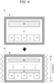
- Figs. 4 and 5 are explanatory views for explaining the crystal growth step S30 according to the embodiment.
- the crystal growth step S30 is a step in which the SiC underlying substrate 10 and a semiconductor material 40 serving as the source of the AlN layer 20 are disposed and heated in such a way as facing (confronting) each other in a crucible 30 having a quasi-closed space.
- the "quasi-closed space” in the present description refers to a space in which inside of the container can be evacuated but at least a part of the steam generated in the container can be confined.
- the crystal growth step S30 is a step of heating such that the temperature gradient is formed along the vertical direction of the SiC underlying substrate 10.
- the source is transported from the semiconductor material 40 onto the SiC underlying substrate 10 via a source transport space 31.
- the temperature gradient described above and a chemical potential difference between the SiC underlying substrate 10 and the semiconductor material 40 can be adopted.
- a vapor composed of an element sublimated from the semiconductor material 40 is transported by diffusing in the source transport space 31, and is supersaturated and condensed on the SiC underlying substrate 10 set to have a temperature lower than that of the semiconductor material 40.
- the AlN layer 20 is formed on the SiC underlying substrate 10.
- the crystal growth step S30 includes a lateral growth step S31 in which the AlN layer 20 grows in the horizontal direction of the SiC underlying substrate 10 and a longitudinal growth step S32 in which the AlN layer 20 grows in the vertical direction of the SiC underlying substrate 10.
- the lateral growth step S31 may include a growth component in the vertical direction as long as the growth component in the horizontal direction is larger than the growth component in the vertical direction (growth component: horizontal direction > vertical direction).
- the longitudinal growth step S32 may include a growth component in the horizontal direction as long as the growth component in the vertical direction is larger than the growth component in the horizontal direction (growth component: vertical direction > horizontal direction).
- the lateral growth step S31 is a step in which the AlN layer 20 grows toward the through holes 11 by the heat escaping from the through holes 11 of the SiC underlying substrate 10 to form the temperature gradient in the horizontal direction on the surface of the SiC underlying substrate 10.
- an inert gas or a doping gas may be introduced into the source transport space 31 to control the doping concentration and growth environment of the AlN layer 20.
- a large-diameter AlN substrate can be manufactured by crystal-growing the AlN layer 20 on the SiC underlying substrate 10 having the through holes 11.
- the heat escapes from the region where the through holes 11 are formed, so that a growth driving force acts in the horizontal direction of the SiC underlying substrate 10.
- the AlN layer 20 is promoted on the region where the through holes 11 are formed, and the AlN layer 20 having a diameter equivalent to that of the SiC underlying substrate 10 can be formed. Therefore, by adopting the SiC underlying substrate 10 having a large diameter, the AlN substrate having a large diameter can be obtained.
- the crystallinity of the AlN layer 20 can be improved by forming the AlN layer 20 on the region where the through holes 11 are formed.
- the AlN layer 20 formed on the region where the through holes 11 are formed is not located immediately above the SiC underlying substrate 10. Therefore, it is possible to reduce a dislocation of a threading system in the AlN layer 20 without taking over the dislocation (for example, threading screw dislocations, threading edge dislocations, micropipes, and the like) of the threading system existing in the SiC underlying substrate 10.
- the SiC underlying substrate 10 was irradiated with a laser under the following conditions to form the through holes 11.
- Fig. 6 is an explanatory view for explaining a pattern of the through holes 11 formed in the through hole formation step S10 according to Example 1.
- Fig. 6(a) is an explanatory view illustrating a state in which the plurality of through holes 11 is arranged.
- black regions indicate a portion of the through holes 11, and white regions remain as the SiC underlying substrate 10.
- Fig. 6(b) is an explanatory view illustrating a state in which the through holes 11 of Fig. 6(a) are enlarged.
- white regions indicate a portion of the through holes 11, and black regions remain as the SiC underlying substrate 10.
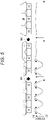
- Fig. 7 is an explanatory view for explaining the strained layer removal step S20 according to Example 1.
- the SiC underlying substrate 10 having the through holes 11 formed in the through hole formation step S10 was housed in a SiC container 50, the SiC container 50 was housed in a TaC container 60, and they were heated under the following conditions.
- the SiC container 50 is a fitting container including an upper container 51 and a lower container 52 that can be fitted to each other.
- a gap 53 is formed in a fitting portion between the upper container 51 and the lower container 52, and the SiC container 50 can be exhausted (evacuated) from the gap 53.
- the SiC container 50 has an etching space 54 formed by making a part of the SiC container 50 arranged on the low temperature side of the temperature gradient face the SiC underlying substrate 10 in a state where the SiC underlying substrate 10 is arranged on the high temperature side of the temperature gradient.
- the etching space 54 is a space for transporting and etching Si atoms and C atoms from the SiC underlying substrate 10 to the SiC container 50 using a temperature difference provided between the SiC underlying substrate 10 and the bottom surface of the SiC container 50 as the driving force.
- the SiC container 50 includes a substrate holder 55 that holds the SiC underlying substrate 10 in a hollow state to form the etching space 54.
- the substrate holder 55 may not be provided depending on a direction of the temperature gradient of a heating furnace. For example, when the heating furnace forms a temperature gradient such that the temperature becomes lower from the lower container 52 toward the upper container 51, the SiC underlying substrate 10 may be disposed on the bottom surface of the lower container 52 without providing the substrate holder 55.
- the TaC container 60 is a fitting container including an upper container 61 and a lower container 62 that can be fitted to each other, and is configured to be able to house the SiC container 50.
- a gap 63 is formed in a fitting portion between the upper container 61 and the lower container 62, and the TaC container 60 can be exhausted (evacuated) from the gap 63.
- the TaC container 60 includes the Si vapor supply source 64 capable of supplying vapor pressure of a vapor phase type containing Si element into the TaC container 60.
- the Si vapor supply source 64 may be configured to generate vapor pressure of the vapor phase type containing Si element in the TaC container 60 during heat treatment.
- Fig. 8 is an explanatory view for explaining the crystal growth step S30 according to Example 1.
- the SiC underlying substrate 10 from which the strained layer 12 has been removed in the strained layer removal step S20 was housed in the crucible 30 while facing the semiconductor material 40, and was heated under the following conditions.
- the crucible 30 has a source transport space 31 between the SiC underlying substrate 10 and the semiconductor material 40.
- the source is transported from the semiconductor material 40 onto the SiC underlying substrate 10 through the source transport space 31.
- Fig. 8(a) is an example of the crucible 30 to be used in the crystal growth step S30.
- the crucible 30 is a fitting container including an upper container 32 and a lower container 33 that can be fitted to each other.
- a gap 34 is formed in a fitting portion between the upper container 32 and the lower container 33, and the crucible 30 can be exhausted (evacuated) from the gap 34.
- the crucible 30 includes a substrate holder 35 that forms the source transport space 31.
- the substrate holder 35 is provided between the SiC underlying substrate 10 and the semiconductor material 40, and forms the source transport space 31 by arranging the semiconductor material 40 on the high temperature side and the SiC underlying substrate 10 on the low temperature side.
- Figs. 8(b) and 8(c) are another example of the crucible 30 to be used in the crystal growth step S30.
- the temperature gradient in Figs. 8(b) and 8(c) is set opposite to the temperature gradient in Fig. 8(a) , and the SiC underlying substrate 10 is disposed on an upper side.
- the semiconductor material 40 is disposed on the high temperature side, and the SiC underlying substrate 10 is disposed on the low temperature side to form the source transport space 31.
- Fig. 8(b) illustrates an example in which the SiC underlying substrate 10 is fixed to the upper container 32 side to form the source transport space 31 with the semiconductor material 40.
- Fig. 8(c) illustrates an example in which the source transport space 31 is formed between the semiconductor material 40 and the SiC underlying substrate 10 by forming a through window in the upper container 32 and arranging the underlying substrate. Furthermore, as illustrated in Fig. 8(c) , an intermediate member 36 may be provided between the upper container 32 and the lower container 33 to form the source transport space 31.
- the AlN sintered body of the semiconductor material 40 was sintered in the following procedure.
- the AlN powder was placed in a frame of a TaC block and compacted with an appropriate force. Thereafter, the compacted AlN powder and the TaC block were housed in a thermal decomposition carbon crucible and heated under the following conditions.
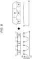
- Fig. 9 is a schematic view showing a crystal growth step S30 of Example 1.
- the temperature gradient can be formed in the horizontal direction of the SiC underlying substrate 10 and used as a driving force for the lateral growth of the AlN layer 20.
- the AlN layer 20 can be formed on the region where the through holes 11 are formed, and a large-diameter AlN substrate can be manufactured.
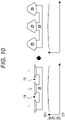
- a groove 13 was formed instead of the through holes 11 of Example 1.
- the SiC underlying substrate 10 was subjected to the crystal growth step S30 under the same conditions as in Example 1. In other words, in Comparative Example 1, the crystal growth step S30 was performed without performing the through hole formation step S10.
- Fig. 10 is a schematic view showing the crystal growth step S30 of Comparative Example 1.
- a region in which the AlN layer 20 did not grow was formed on the groove 13.
- the temperature in the region of the groove 13 does not become lower, and the temperature gradient is not formed in the horizontal direction of the SiC underlying substrate 10. As a result, it is considered that the growth driving force in the lateral direction is not generated and the AlN layer 20 is not formed in the region of the groove 13.
- Example 1 it can be understood that a large-diameter AlN substrate can be manufactured by forming the AlN layer 20 on the SiC underlying substrate 10 having the through holes 11.
Landscapes
- Chemical & Material Sciences (AREA)
- Engineering & Computer Science (AREA)
- Crystallography & Structural Chemistry (AREA)
- Materials Engineering (AREA)
- Metallurgy (AREA)
- Organic Chemistry (AREA)
- Inorganic Chemistry (AREA)
- Chemical Kinetics & Catalysis (AREA)
- General Chemical & Material Sciences (AREA)
- Crystals, And After-Treatments Of Crystals (AREA)
Applications Claiming Priority (2)
| Application Number | Priority Date | Filing Date | Title |
|---|---|---|---|
| JP2020072550 | 2020-04-14 | ||
| PCT/JP2021/013746 WO2021210393A1 (fr) | 2020-04-14 | 2021-03-30 | Procédé de fabrication d'un substrat de nitrure d'aluminium, substrat de nitrure d'aluminium et procédé de formation d'une couche de nitrure d'aluminium |
Publications (2)
| Publication Number | Publication Date |
|---|---|
| EP4137623A1 true EP4137623A1 (fr) | 2023-02-22 |
| EP4137623A4 EP4137623A4 (fr) | 2024-05-22 |
Family
ID=78084194
Family Applications (1)
| Application Number | Title | Priority Date | Filing Date |
|---|---|---|---|
| EP21789219.9A Pending EP4137623A4 (fr) | 2020-04-14 | 2021-03-30 | Procédé de fabrication d'un substrat de nitrure d'aluminium, substrat de nitrure d'aluminium et procédé de formation d'une couche de nitrure d'aluminium |
Country Status (5)
| Country | Link |
|---|---|
| US (1) | US12509795B2 (fr) |
| EP (1) | EP4137623A4 (fr) |
| JP (1) | JP7758909B2 (fr) |
| TW (1) | TWI885113B (fr) |
| WO (1) | WO2021210393A1 (fr) |
Families Citing this family (2)
| Publication number | Priority date | Publication date | Assignee | Title |
|---|---|---|---|---|
| WO2021210392A1 (fr) * | 2020-04-14 | 2021-10-21 | 学校法人関西学院 | Procédé de fabrication de substrat semi-conducteur, substrat semi-conducteur et procédé de formation de couche obtenue par croissance |
| TWI882241B (zh) * | 2022-05-05 | 2025-05-01 | 環球晶圓股份有限公司 | 磊晶結構及其製造方法 |
Family Cites Families (11)
| Publication number | Priority date | Publication date | Assignee | Title |
|---|---|---|---|---|
| US6579359B1 (en) | 1999-06-02 | 2003-06-17 | Technologies And Devices International, Inc. | Method of crystal growth and resulted structures |
| JP4072352B2 (ja) * | 2002-02-05 | 2008-04-09 | 住友電気工業株式会社 | 窒化物系化合物半導体素子及びその作製方法 |
| JP5186733B2 (ja) | 2005-07-29 | 2013-04-24 | 住友電気工業株式会社 | AlN結晶の成長方法 |
| EP2000567B1 (fr) * | 2006-03-29 | 2014-12-31 | Sumitomo Electric Industries, Ltd. | Procede de croissance d'un monocristal de iii nitrure |
| JP5262201B2 (ja) * | 2008-03-10 | 2013-08-14 | 富士通株式会社 | 半導体装置の製造方法 |
| JP6241286B2 (ja) | 2014-01-14 | 2017-12-06 | 住友電気工業株式会社 | 炭化珪素単結晶の製造方法 |
| JP6384851B2 (ja) * | 2014-03-03 | 2018-09-05 | 国立大学法人大阪大学 | Iii族窒化物結晶の製造方法、iii族窒化物結晶、半導体装置およびiii族窒化物結晶製造装置 |
| JP6183317B2 (ja) * | 2014-08-08 | 2017-08-23 | 豊田合成株式会社 | Iii族窒化物半導体の製造方法及びiii族窒化物半導体ウエハ |
| WO2016147786A1 (fr) | 2015-03-18 | 2016-09-22 | 住友化学株式会社 | Substrat de croissance de semi-conducteur à base de nitrure et procédé pour le fabriquer, et dispositif semi-conducteur et procédé de fabrication correspondant |
| JP6949358B2 (ja) * | 2017-07-28 | 2021-10-13 | 学校法人関西学院 | 単結晶SiCの製造方法、SiCインゴットの製造方法、及びSiCウエハの製造方法 |
| JP6455575B2 (ja) * | 2017-09-12 | 2019-01-23 | 三菱ケミカル株式会社 | 第13族金属窒化物基板の製造方法 |
-
2021
- 2021-03-30 TW TW110111480A patent/TWI885113B/zh active
- 2021-03-30 US US17/996,189 patent/US12509795B2/en active Active
- 2021-03-30 WO PCT/JP2021/013746 patent/WO2021210393A1/fr not_active Ceased
- 2021-03-30 JP JP2022515288A patent/JP7758909B2/ja active Active
- 2021-03-30 EP EP21789219.9A patent/EP4137623A4/fr active Pending
Also Published As
| Publication number | Publication date |
|---|---|
| EP4137623A4 (fr) | 2024-05-22 |
| TWI885113B (zh) | 2025-06-01 |
| WO2021210393A1 (fr) | 2021-10-21 |
| US20230304186A1 (en) | 2023-09-28 |
| TW202144630A (zh) | 2021-12-01 |
| CN115443352A (zh) | 2022-12-06 |
| JP7758909B2 (ja) | 2025-10-23 |
| JPWO2021210393A1 (fr) | 2021-10-21 |
| US12509795B2 (en) | 2025-12-30 |
Similar Documents
| Publication | Publication Date | Title |
|---|---|---|
| US20060254505A1 (en) | Method and apparatus for the production of silicon carbide crystals | |
| EP2126163A2 (fr) | Procédé de croissance par sublimation sic à diamètre guide au moyen d'un guide de croissance multi-couches | |
| KR100845946B1 (ko) | SiC 단결정 성장방법 | |
| EP4137623A1 (fr) | Procédé de fabrication d'un substrat de nitrure d'aluminium, substrat de nitrure d'aluminium et procédé de formation d'une couche de nitrure d'aluminium | |
| US12255073B2 (en) | Silicon carbide substrate manufacturing method, silicon carbide substrate, and method of removing strain layer introduced into silicon carbide substrate by laser processing | |
| EP4137622A1 (fr) | Procédé de production d'un substrat semi-conducteur, substrat semi-conducteur et procédé de prévention de l'apparition de fissures dans une couche de croissance | |
| KR20080030570A (ko) | AlN 결정 및 그 성장 방법과 AlN 결정 기판 | |
| EP4137614A1 (fr) | Procédé de production de substrat de nitrure d'aluminium, substrat de nitrure d'aluminium et procédé pour supprimer l'apparition de fissures dans une couche de nitrure d'aluminium | |
| EP4137616A1 (fr) | Procédé de production d'un substrat de nitrure d'aluminium, substrat de nitrure d'aluminium et procédé pour supprimer l'introduction d'une dislocation dans une couche de croissance de nitrure d'aluminium | |
| US12385158B2 (en) | Method for manufacturing a semiconductor substrate by forming a growth layer on an underlying substrate having through holes | |
| CN115443352B (en) | Method for manufacturing aluminum nitride substrate, and method for forming aluminum nitride layer | |
| US12460315B2 (en) | Method for manufacturing semiconductor substrates and method for suppressing introduction of displacement to growth layer |
Legal Events
| Date | Code | Title | Description |
|---|---|---|---|
| STAA | Information on the status of an ep patent application or granted ep patent |
Free format text: STATUS: THE INTERNATIONAL PUBLICATION HAS BEEN MADE |
|
| PUAI | Public reference made under article 153(3) epc to a published international application that has entered the european phase |
Free format text: ORIGINAL CODE: 0009012 |
|
| STAA | Information on the status of an ep patent application or granted ep patent |
Free format text: STATUS: REQUEST FOR EXAMINATION WAS MADE |
|
| 17P | Request for examination filed |
Effective date: 20221107 |
|
| AK | Designated contracting states |
Kind code of ref document: A1 Designated state(s): AL AT BE BG CH CY CZ DE DK EE ES FI FR GB GR HR HU IE IS IT LI LT LU LV MC MK MT NL NO PL PT RO RS SE SI SK SM TR |
|
| DAV | Request for validation of the european patent (deleted) | ||
| DAX | Request for extension of the european patent (deleted) | ||
| A4 | Supplementary search report drawn up and despatched |
Effective date: 20240418 |
|
| RIC1 | Information provided on ipc code assigned before grant |
Ipc: C30B 33/08 20060101ALI20240412BHEP Ipc: C30B 29/40 20060101ALI20240412BHEP Ipc: C30B 25/18 20060101ALI20240412BHEP Ipc: C30B 23/02 20060101ALI20240412BHEP Ipc: C30B 23/06 20060101ALI20240412BHEP Ipc: C30B 29/38 20060101AFI20240412BHEP |