JP5262201B2 - 半導体装置の製造方法 - Google Patents
半導体装置の製造方法 Download PDFInfo
- Publication number
- JP5262201B2 JP5262201B2 JP2008060148A JP2008060148A JP5262201B2 JP 5262201 B2 JP5262201 B2 JP 5262201B2 JP 2008060148 A JP2008060148 A JP 2008060148A JP 2008060148 A JP2008060148 A JP 2008060148A JP 5262201 B2 JP5262201 B2 JP 5262201B2
- Authority
- JP
- Japan
- Prior art keywords
- layer
- gan
- substrate
- manufacturing
- semiconductor device
- Prior art date
- Legal status (The legal status is an assumption and is not a legal conclusion. Google has not performed a legal analysis and makes no representation as to the accuracy of the status listed.)
- Expired - Fee Related
Links
Images


Landscapes
- Weting (AREA)
- Junction Field-Effect Transistors (AREA)
- Recrystallisation Techniques (AREA)
- Chemical Vapour Deposition (AREA)
- Electrodes Of Semiconductors (AREA)
Description
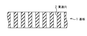
先ず、第1の実施形態について説明する。図1A乃至図1Tは、第1の実施形態に係るGaN系HEMT(半導体装置)を製造する方法を工程順に示す断面図である。
次に、第2の実施形態について説明する。図6A乃至図6Bは、第2の実施形態に係るGaN系HEMT(半導体装置)を製造する方法を工程順に示す断面図である。
次に、第3の実施形態について説明する。図7A乃至図7Fは、第3の実施形態に係るGaN系HEMT(半導体装置)を製造する方法を工程順に示す断面図である。
2:貫通穴
3:AlN層
4:GaN層
5:i−AlGaN層
6:n−AlGaN層
7:n−GaN層
9d:ドレイン電極
9g:ゲート電極
9s:ソース電極
10:パッシベーション膜
12:パッシベーション膜
21:基板
22:基板
62:基板
Claims (5)
- 貫通穴が形成された結晶成長基板の一方の面上に化合物半導体結晶層を形成して前記貫通穴の開口部を消失させる工程と、
所定のエッチング溶液を前記貫通穴に侵入させると共に、前記結晶成長基板に紫外線を照射することにより、前記化合物半導体結晶層を前記結晶成長基板から分離する工程と、
を有することを特徴とする半導体装置の製造方法。 - 前記化合物半導体結晶層として、窒化物半導体結晶層を用いることを特徴とする請求項1に記載の半導体装置の製造方法。
- 前記窒化物半導体結晶層として、GaN、AlN及びInNからなる群から選択された一種又は二種以上の混晶からなるものを用いることを特徴とする請求項2に記載の半導体装置の製造方法。
- 前記結晶成長基板として、SiC基板を用いることを特徴とする請求項1乃至3のいずれか1項に記載の半導体装置の製造方法。
- 前記分離する工程の後、前記化合物半導体結晶層に基板を貼り付ける工程を更に有することを特徴とする請求項1乃至4のいずれか1項に記載の半導体装置の製造方法。
Priority Applications (1)
| Application Number | Priority Date | Filing Date | Title |
|---|---|---|---|
| JP2008060148A JP5262201B2 (ja) | 2008-03-10 | 2008-03-10 | 半導体装置の製造方法 |
Applications Claiming Priority (1)
| Application Number | Priority Date | Filing Date | Title |
|---|---|---|---|
| JP2008060148A JP5262201B2 (ja) | 2008-03-10 | 2008-03-10 | 半導体装置の製造方法 |
Publications (2)
| Publication Number | Publication Date |
|---|---|
| JP2009218370A JP2009218370A (ja) | 2009-09-24 |
| JP5262201B2 true JP5262201B2 (ja) | 2013-08-14 |
Family
ID=41189957
Family Applications (1)
| Application Number | Title | Priority Date | Filing Date |
|---|---|---|---|
| JP2008060148A Expired - Fee Related JP5262201B2 (ja) | 2008-03-10 | 2008-03-10 | 半導体装置の製造方法 |
Country Status (1)
| Country | Link |
|---|---|
| JP (1) | JP5262201B2 (ja) |
Families Citing this family (6)
| Publication number | Priority date | Publication date | Assignee | Title |
|---|---|---|---|---|
| JP5433909B2 (ja) * | 2012-05-22 | 2014-03-05 | 株式会社パウデック | GaN系半導体素子の製造方法 |
| CN105140122B (zh) * | 2015-08-10 | 2018-07-20 | 中国电子科技集团公司第五十五研究所 | 一种改善GaN HEMT器件散热性能的方法 |
| JP6875634B2 (ja) * | 2017-04-27 | 2021-05-26 | 富士通株式会社 | 半導体装置及びその製造方法 |
| JP6912716B2 (ja) * | 2017-08-10 | 2021-08-04 | 富士通株式会社 | 半導体装置及びその製造方法 |
| TWI885113B (zh) * | 2020-04-14 | 2025-06-01 | 學校法人關西學院 | 氮化鋁基板的製造方法、氮化鋁基板以及氮化鋁層的形成方法 |
| CN113889411B (zh) * | 2021-09-14 | 2023-11-14 | 北京科技大学 | 一种带金刚石微柱阵列的金刚石基GaN材料制备方法 |
Family Cites Families (4)
| Publication number | Priority date | Publication date | Assignee | Title |
|---|---|---|---|---|
| US6265289B1 (en) * | 1998-06-10 | 2001-07-24 | North Carolina State University | Methods of fabricating gallium nitride semiconductor layers by lateral growth from sidewalls into trenches, and gallium nitride semiconductor structures fabricated thereby |
| JP2002289541A (ja) * | 2001-03-27 | 2002-10-04 | Toshiba Corp | GaN系半導体結晶の形成方法及びその結晶を用いたGaN系半導体素子の製造方法 |
| US6617261B2 (en) * | 2001-12-18 | 2003-09-09 | Xerox Corporation | Structure and method for fabricating GaN substrates from trench patterned GaN layers on sapphire substrates |
| JP2007214500A (ja) * | 2006-02-13 | 2007-08-23 | Mitsubishi Chemicals Corp | 半導体部材及びその製造方法 |
-
2008
- 2008-03-10 JP JP2008060148A patent/JP5262201B2/ja not_active Expired - Fee Related
Also Published As
| Publication number | Publication date |
|---|---|
| JP2009218370A (ja) | 2009-09-24 |
Similar Documents
| Publication | Publication Date | Title |
|---|---|---|
| TWI767741B (zh) | 與工程基板整合之電力元件 | |
| US12020931B2 (en) | Method for fabricating field-effect transistor | |
| KR101008272B1 (ko) | 노멀 오프 특성을 갖는 질화물계 고전자 이동도 트랜지스터및 그 제조방법 | |
| US20050269671A1 (en) | Support for hybrid epitaxy and method of fabrication | |
| JP5397042B2 (ja) | 半導体装置の製造方法 | |
| JP7052503B2 (ja) | トランジスタの製造方法 | |
| JP2021506116A (ja) | 加工基板上の集積デバイスのためのシステムおよび方法 | |
| JP5161759B2 (ja) | 化合物半導体装置の製造方法 | |
| JP2012094688A (ja) | 半導体装置およびその製造方法 | |
| JP5262201B2 (ja) | 半導体装置の製造方法 | |
| WO2017144852A1 (en) | Layered vertical field effect transistor and methods of fabrication | |
| JP2016139655A (ja) | 半導体装置及び半導体装置の製造方法 | |
| JP2017228577A (ja) | 化合物半導体装置の製造方法 | |
| JP5401788B2 (ja) | 窒化物半導体装置及びその製造方法 | |
| JP2010192872A (ja) | 半導体基板の製造方法、半導体デバイスの製造方法、半導体基板および半導体デバイス | |
| JP2017228578A (ja) | エピ基板 | |
| CN113628963A (zh) | Ⅲ族氮化物增强型hemt器件及其制造方法 | |
| JP4822457B2 (ja) | 半導体装置の製造方法 | |
| JP2012243792A (ja) | GaN薄膜貼り合わせ基板およびその製造方法、ならびにGaN系高電子移動度トランジスタおよびその製造方法 | |
| JP5564799B2 (ja) | 窒化ガリウム系半導体電子デバイスを作製する方法 | |
| CN113628962A (zh) | Ⅲ族氮化物增强型hemt器件及其制造方法 | |
| KR101943356B1 (ko) | 선택 성장을 이용한 질화물 반도체 소자 및 그 제조 방법 | |
| KR20130008281A (ko) | 파워소자의 제조방법 | |
| JP2009302191A (ja) | 半導体装置及びその製造方法 | |
| JP6783063B2 (ja) | 窒化物半導体テンプレートおよび窒化物半導体積層物 |
Legal Events
| Date | Code | Title | Description |
|---|---|---|---|
| A621 | Written request for application examination |
Free format text: JAPANESE INTERMEDIATE CODE: A621 Effective date: 20100416 |
|
| A977 | Report on retrieval |
Free format text: JAPANESE INTERMEDIATE CODE: A971007 Effective date: 20121009 |
|
| A131 | Notification of reasons for refusal |
Free format text: JAPANESE INTERMEDIATE CODE: A131 Effective date: 20121016 |
|
| A521 | Written amendment |
Free format text: JAPANESE INTERMEDIATE CODE: A523 Effective date: 20121205 |
|
| TRDD | Decision of grant or rejection written | ||
| A01 | Written decision to grant a patent or to grant a registration (utility model) |
Free format text: JAPANESE INTERMEDIATE CODE: A01 Effective date: 20130402 |
|
| A61 | First payment of annual fees (during grant procedure) |
Free format text: JAPANESE INTERMEDIATE CODE: A61 Effective date: 20130415 |
|
| R150 | Certificate of patent or registration of utility model |
Free format text: JAPANESE INTERMEDIATE CODE: R150 Ref document number: 5262201 Country of ref document: JP Free format text: JAPANESE INTERMEDIATE CODE: R150 |
|
| LAPS | Cancellation because of no payment of annual fees |