EP4145519A1 - Substrat d'affichage et dispositif d'affichage - Google Patents
Substrat d'affichage et dispositif d'affichage Download PDFInfo
- Publication number
- EP4145519A1 EP4145519A1 EP20904234.0A EP20904234A EP4145519A1 EP 4145519 A1 EP4145519 A1 EP 4145519A1 EP 20904234 A EP20904234 A EP 20904234A EP 4145519 A1 EP4145519 A1 EP 4145519A1
- Authority
- EP
- European Patent Office
- Prior art keywords
- anode
- base substrate
- main body
- orthographic projection
- region
- Prior art date
- Legal status (The legal status is an assumption and is not a legal conclusion. Google has not performed a legal analysis and makes no representation as to the accuracy of the status listed.)
- Pending
Links
Images


Classifications
-
- G—PHYSICS
- G09—EDUCATION; CRYPTOGRAPHY; DISPLAY; ADVERTISING; SEALS
- G09G—ARRANGEMENTS OR CIRCUITS FOR CONTROL OF INDICATING DEVICES USING STATIC MEANS TO PRESENT VARIABLE INFORMATION
- G09G3/00—Control arrangements or circuits, of interest only in connection with visual indicators other than cathode-ray tubes
- G09G3/20—Control arrangements or circuits, of interest only in connection with visual indicators other than cathode-ray tubes for presentation of an assembly of a number of characters, e.g. a page, by composing the assembly by combination of individual elements arranged in a matrix no fixed position being assigned to or needed to be assigned to the individual characters or partial characters
- G09G3/22—Control arrangements or circuits, of interest only in connection with visual indicators other than cathode-ray tubes for presentation of an assembly of a number of characters, e.g. a page, by composing the assembly by combination of individual elements arranged in a matrix no fixed position being assigned to or needed to be assigned to the individual characters or partial characters using controlled light sources
- G09G3/30—Control arrangements or circuits, of interest only in connection with visual indicators other than cathode-ray tubes for presentation of an assembly of a number of characters, e.g. a page, by composing the assembly by combination of individual elements arranged in a matrix no fixed position being assigned to or needed to be assigned to the individual characters or partial characters using controlled light sources using electroluminescent panels
- G09G3/32—Control arrangements or circuits, of interest only in connection with visual indicators other than cathode-ray tubes for presentation of an assembly of a number of characters, e.g. a page, by composing the assembly by combination of individual elements arranged in a matrix no fixed position being assigned to or needed to be assigned to the individual characters or partial characters using controlled light sources using electroluminescent panels semiconductive, e.g. using light-emitting diodes [LED]
- G09G3/3208—Control arrangements or circuits, of interest only in connection with visual indicators other than cathode-ray tubes for presentation of an assembly of a number of characters, e.g. a page, by composing the assembly by combination of individual elements arranged in a matrix no fixed position being assigned to or needed to be assigned to the individual characters or partial characters using controlled light sources using electroluminescent panels semiconductive, e.g. using light-emitting diodes [LED] organic, e.g. using organic light-emitting diodes [OLED]
- G09G3/3225—Control arrangements or circuits, of interest only in connection with visual indicators other than cathode-ray tubes for presentation of an assembly of a number of characters, e.g. a page, by composing the assembly by combination of individual elements arranged in a matrix no fixed position being assigned to or needed to be assigned to the individual characters or partial characters using controlled light sources using electroluminescent panels semiconductive, e.g. using light-emitting diodes [LED] organic, e.g. using organic light-emitting diodes [OLED] using an active matrix
- G09G3/3233—Control arrangements or circuits, of interest only in connection with visual indicators other than cathode-ray tubes for presentation of an assembly of a number of characters, e.g. a page, by composing the assembly by combination of individual elements arranged in a matrix no fixed position being assigned to or needed to be assigned to the individual characters or partial characters using controlled light sources using electroluminescent panels semiconductive, e.g. using light-emitting diodes [LED] organic, e.g. using organic light-emitting diodes [OLED] using an active matrix with pixel circuitry controlling the current through the light-emitting element
- G09G3/3241—Control arrangements or circuits, of interest only in connection with visual indicators other than cathode-ray tubes for presentation of an assembly of a number of characters, e.g. a page, by composing the assembly by combination of individual elements arranged in a matrix no fixed position being assigned to or needed to be assigned to the individual characters or partial characters using controlled light sources using electroluminescent panels semiconductive, e.g. using light-emitting diodes [LED] organic, e.g. using organic light-emitting diodes [OLED] using an active matrix with pixel circuitry controlling the current through the light-emitting element the current through the light-emitting element being set using a data current provided by the data driver, e.g. by using a two-transistor current mirror
-
- H—ELECTRICITY
- H10—SEMICONDUCTOR DEVICES; ELECTRIC SOLID-STATE DEVICES NOT OTHERWISE PROVIDED FOR
- H10K—ORGANIC ELECTRIC SOLID-STATE DEVICES
- H10K59/00—Integrated devices, or assemblies of multiple devices, comprising at least one organic light-emitting element covered by group H10K50/00
- H10K59/10—OLED displays
- H10K59/12—Active-matrix OLED [AMOLED] displays
-
- G—PHYSICS
- G09—EDUCATION; CRYPTOGRAPHY; DISPLAY; ADVERTISING; SEALS
- G09F—DISPLAYING; ADVERTISING; SIGNS; LABELS OR NAME-PLATES; SEALS
- G09F9/00—Indicating arrangements for variable information in which the information is built-up on a support by selection or combination of individual elements
- G09F9/30—Indicating arrangements for variable information in which the information is built-up on a support by selection or combination of individual elements in which the desired character or characters are formed by combining individual elements
- G09F9/33—Indicating arrangements for variable information in which the information is built-up on a support by selection or combination of individual elements in which the desired character or characters are formed by combining individual elements being semiconductor devices, e.g. diodes
- G09F9/335—Indicating arrangements for variable information in which the information is built-up on a support by selection or combination of individual elements in which the desired character or characters are formed by combining individual elements being semiconductor devices, e.g. diodes being organic light emitting diodes [OLED]
-
- H—ELECTRICITY
- H10—SEMICONDUCTOR DEVICES; ELECTRIC SOLID-STATE DEVICES NOT OTHERWISE PROVIDED FOR
- H10D—INORGANIC ELECTRIC SEMICONDUCTOR DEVICES
- H10D84/00—Integrated devices formed in or on semiconductor substrates that comprise only semiconducting layers, e.g. on Si wafers or on GaAs-on-Si wafers
- H10D84/01—Manufacture or treatment
-
- H—ELECTRICITY
- H10—SEMICONDUCTOR DEVICES; ELECTRIC SOLID-STATE DEVICES NOT OTHERWISE PROVIDED FOR
- H10K—ORGANIC ELECTRIC SOLID-STATE DEVICES
- H10K50/00—Organic light-emitting devices
- H10K50/80—Constructional details
- H10K50/805—Electrodes
- H10K50/81—Anodes
- H10K50/813—Anodes characterised by their shape
-
- H—ELECTRICITY
- H10—SEMICONDUCTOR DEVICES; ELECTRIC SOLID-STATE DEVICES NOT OTHERWISE PROVIDED FOR
- H10K—ORGANIC ELECTRIC SOLID-STATE DEVICES
- H10K59/00—Integrated devices, or assemblies of multiple devices, comprising at least one organic light-emitting element covered by group H10K50/00
- H10K59/10—OLED displays
- H10K59/12—Active-matrix OLED [AMOLED] displays
- H10K59/122—Pixel-defining structures or layers, e.g. banks
-
- H—ELECTRICITY
- H10—SEMICONDUCTOR DEVICES; ELECTRIC SOLID-STATE DEVICES NOT OTHERWISE PROVIDED FOR
- H10K—ORGANIC ELECTRIC SOLID-STATE DEVICES
- H10K59/00—Integrated devices, or assemblies of multiple devices, comprising at least one organic light-emitting element covered by group H10K50/00
- H10K59/10—OLED displays
- H10K59/12—Active-matrix OLED [AMOLED] displays
- H10K59/126—Shielding, e.g. light-blocking means over the TFTs
-
- H—ELECTRICITY
- H10—SEMICONDUCTOR DEVICES; ELECTRIC SOLID-STATE DEVICES NOT OTHERWISE PROVIDED FOR
- H10K—ORGANIC ELECTRIC SOLID-STATE DEVICES
- H10K59/00—Integrated devices, or assemblies of multiple devices, comprising at least one organic light-emitting element covered by group H10K50/00
- H10K59/10—OLED displays
- H10K59/12—Active-matrix OLED [AMOLED] displays
- H10K59/131—Interconnections, e.g. wiring lines or terminals
-
- H—ELECTRICITY
- H10—SEMICONDUCTOR DEVICES; ELECTRIC SOLID-STATE DEVICES NOT OTHERWISE PROVIDED FOR
- H10K—ORGANIC ELECTRIC SOLID-STATE DEVICES
- H10K59/00—Integrated devices, or assemblies of multiple devices, comprising at least one organic light-emitting element covered by group H10K50/00
- H10K59/30—Devices specially adapted for multicolour light emission
- H10K59/35—Devices specially adapted for multicolour light emission comprising red-green-blue [RGB] subpixels
-
- H—ELECTRICITY
- H10—SEMICONDUCTOR DEVICES; ELECTRIC SOLID-STATE DEVICES NOT OTHERWISE PROVIDED FOR
- H10K—ORGANIC ELECTRIC SOLID-STATE DEVICES
- H10K59/00—Integrated devices, or assemblies of multiple devices, comprising at least one organic light-emitting element covered by group H10K50/00
- H10K59/80—Constructional details
- H10K59/805—Electrodes
- H10K59/8051—Anodes
- H10K59/80515—Anodes characterised by their shape
-
- G—PHYSICS
- G09—EDUCATION; CRYPTOGRAPHY; DISPLAY; ADVERTISING; SEALS
- G09G—ARRANGEMENTS OR CIRCUITS FOR CONTROL OF INDICATING DEVICES USING STATIC MEANS TO PRESENT VARIABLE INFORMATION
- G09G2300/00—Aspects of the constitution of display devices
- G09G2300/04—Structural and physical details of display devices
- G09G2300/0421—Structural details of the set of electrodes
- G09G2300/0426—Layout of electrodes and connections
-
- G—PHYSICS
- G09—EDUCATION; CRYPTOGRAPHY; DISPLAY; ADVERTISING; SEALS
- G09G—ARRANGEMENTS OR CIRCUITS FOR CONTROL OF INDICATING DEVICES USING STATIC MEANS TO PRESENT VARIABLE INFORMATION
- G09G2300/00—Aspects of the constitution of display devices
- G09G2300/04—Structural and physical details of display devices
- G09G2300/0469—Details of the physics of pixel operation
-
- G—PHYSICS
- G09—EDUCATION; CRYPTOGRAPHY; DISPLAY; ADVERTISING; SEALS
- G09G—ARRANGEMENTS OR CIRCUITS FOR CONTROL OF INDICATING DEVICES USING STATIC MEANS TO PRESENT VARIABLE INFORMATION
- G09G2300/00—Aspects of the constitution of display devices
- G09G2300/08—Active matrix structure, i.e. with use of active elements, inclusive of non-linear two terminal elements, in the pixels together with light emitting or modulating elements
- G09G2300/0809—Several active elements per pixel in active matrix panels
- G09G2300/0819—Several active elements per pixel in active matrix panels used for counteracting undesired variations, e.g. feedback or autozeroing
-
- G—PHYSICS
- G09—EDUCATION; CRYPTOGRAPHY; DISPLAY; ADVERTISING; SEALS
- G09G—ARRANGEMENTS OR CIRCUITS FOR CONTROL OF INDICATING DEVICES USING STATIC MEANS TO PRESENT VARIABLE INFORMATION
- G09G2300/00—Aspects of the constitution of display devices
- G09G2300/08—Active matrix structure, i.e. with use of active elements, inclusive of non-linear two terminal elements, in the pixels together with light emitting or modulating elements
- G09G2300/0809—Several active elements per pixel in active matrix panels
- G09G2300/0842—Several active elements per pixel in active matrix panels forming a memory circuit, e.g. a dynamic memory with one capacitor
-
- G—PHYSICS
- G09—EDUCATION; CRYPTOGRAPHY; DISPLAY; ADVERTISING; SEALS
- G09G—ARRANGEMENTS OR CIRCUITS FOR CONTROL OF INDICATING DEVICES USING STATIC MEANS TO PRESENT VARIABLE INFORMATION
- G09G3/00—Control arrangements or circuits, of interest only in connection with visual indicators other than cathode-ray tubes
- G09G3/20—Control arrangements or circuits, of interest only in connection with visual indicators other than cathode-ray tubes for presentation of an assembly of a number of characters, e.g. a page, by composing the assembly by combination of individual elements arranged in a matrix no fixed position being assigned to or needed to be assigned to the individual characters or partial characters
- G09G3/22—Control arrangements or circuits, of interest only in connection with visual indicators other than cathode-ray tubes for presentation of an assembly of a number of characters, e.g. a page, by composing the assembly by combination of individual elements arranged in a matrix no fixed position being assigned to or needed to be assigned to the individual characters or partial characters using controlled light sources
- G09G3/30—Control arrangements or circuits, of interest only in connection with visual indicators other than cathode-ray tubes for presentation of an assembly of a number of characters, e.g. a page, by composing the assembly by combination of individual elements arranged in a matrix no fixed position being assigned to or needed to be assigned to the individual characters or partial characters using controlled light sources using electroluminescent panels
- G09G3/32—Control arrangements or circuits, of interest only in connection with visual indicators other than cathode-ray tubes for presentation of an assembly of a number of characters, e.g. a page, by composing the assembly by combination of individual elements arranged in a matrix no fixed position being assigned to or needed to be assigned to the individual characters or partial characters using controlled light sources using electroluminescent panels semiconductive, e.g. using light-emitting diodes [LED]
- G09G3/3208—Control arrangements or circuits, of interest only in connection with visual indicators other than cathode-ray tubes for presentation of an assembly of a number of characters, e.g. a page, by composing the assembly by combination of individual elements arranged in a matrix no fixed position being assigned to or needed to be assigned to the individual characters or partial characters using controlled light sources using electroluminescent panels semiconductive, e.g. using light-emitting diodes [LED] organic, e.g. using organic light-emitting diodes [OLED]
- G09G3/3225—Control arrangements or circuits, of interest only in connection with visual indicators other than cathode-ray tubes for presentation of an assembly of a number of characters, e.g. a page, by composing the assembly by combination of individual elements arranged in a matrix no fixed position being assigned to or needed to be assigned to the individual characters or partial characters using controlled light sources using electroluminescent panels semiconductive, e.g. using light-emitting diodes [LED] organic, e.g. using organic light-emitting diodes [OLED] using an active matrix
- G09G3/3233—Control arrangements or circuits, of interest only in connection with visual indicators other than cathode-ray tubes for presentation of an assembly of a number of characters, e.g. a page, by composing the assembly by combination of individual elements arranged in a matrix no fixed position being assigned to or needed to be assigned to the individual characters or partial characters using controlled light sources using electroluminescent panels semiconductive, e.g. using light-emitting diodes [LED] organic, e.g. using organic light-emitting diodes [OLED] using an active matrix with pixel circuitry controlling the current through the light-emitting element
-
- H—ELECTRICITY
- H10—SEMICONDUCTOR DEVICES; ELECTRIC SOLID-STATE DEVICES NOT OTHERWISE PROVIDED FOR
- H10K—ORGANIC ELECTRIC SOLID-STATE DEVICES
- H10K59/00—Integrated devices, or assemblies of multiple devices, comprising at least one organic light-emitting element covered by group H10K50/00
- H10K59/30—Devices specially adapted for multicolour light emission
- H10K59/35—Devices specially adapted for multicolour light emission comprising red-green-blue [RGB] subpixels
- H10K59/351—Devices specially adapted for multicolour light emission comprising red-green-blue [RGB] subpixels comprising more than three subpixels, e.g. red-green-blue-white [RGBW]
Definitions
- Embodiments of the present disclosure relate to a display substrate and a display device.
- OLED organic light-emitting diode
- Embodiments of the present disclosure provide a display substrate and a display device.
- the display substrate includes: a base substrate; a pixel circuit layer on the base substrate; an anode layer located at a side of the pixel circuit layer away from the base substrate.
- the pixel circuit layer includes a plurality of pixel driving circuits, the anode layer includes a plurality of anodes, the plurality of pixel driving circuits are arranged in one-to-one correspondence with the plurality of anodes, the plurality of anodes include a plurality of anode groups arranged in an array along a first direction and a second direction, each of the plurality of anode groups includes a first anode and a second anode which are oppositely arranged in the second direction.
- the first anode includes a first main body portion and a first connection portion, and the first connection portion is electrically connected to a pixel driving circuit corresponding to the first anode.
- the first anode also includes an extension portion and an anode compensation portion, the orthographic projection of the anode compensation portion on the base substrate covers one thin film transistor in the pixel driving circuit connected to the first connection portion, the first main body portion and the anode compensation portion at least partially overlap in the first direction, the first center line of the anode compensation portion extending in the second direction is located at a first side of the second center line of the first main body portion extending in the second direction.
- the anode compensation portion has a first point at a side away from the second center line, and the first main body portion has a second point at the first side, and the first anode and a connection line between the first point and the second point enclose a notch region, and the area of the notch region is greater than at least one of the area of the anode compensation portion and the area of the first connection portion.
- the shape of the first anode is designed, so that the extension portion of the first anode avoids the light transmitting region of the display substrate as much as possible, thereby improving the light transmittance of the display substrate.
- At least one embodiment of the present disclosure provides a display substrate, which includes: a base substrate; a pixel circuit layer, on the base substrate; an anode layer, at a side of the pixel circuit layer away from the base substrate, wherein the pixel circuit layer includes a plurality of pixel driving circuits, the anode layer includes a plurality of anodes, and the plurality of pixel driving circuits are arranged in one-to-one correspondence with the plurality of anodes, the plurality of anodes include a plurality of anode groups arranged in an array along a first direction and a second direction, each of the plurality of anode groups includes a first anode and a second anode which are oppositely arranged in the second direction, the first anode includes a first main body portion and a first connection portion, and the first connection portion is electrically connected to a pixel driving circuit corresponding to the first anode, the first anode further includes an extension portion and an anode compensation portion, wherein an orthographic
- the area of the notch region is greater than a sum of the area of the anode compensation portion and the area of the first connection portion.
- the anode compensation portion is at the first side of the second center line of the first main body portion extending in the second direction.
- the extension portion includes a first extension portion and a second extension portion, the first extension portion is at a side of the first connection portion away from the first main body portion, the second extension portion is respectively connected to the first extension portion and the anode compensation portion, and the first extension portion is at a side of the second extension portion away from the anode compensation portion.
- a third center line of the first extension portion extending in the second direction is at a second side of the second center line of the first main body portion extending in the second direction, and the second side is opposite to the first side.
- the first extension portion is at the second side of the second center line of the first main body portion extending in the second direction.
- an orthographic projection of the notch region on the base substrate does not overlap with an orthographic projection of the first anode on the base substrate.
- a fourth center line of the first connection portion extending in the second direction is at the first side of the second center line of the first main body portion.
- each of the plurality of pixel driving circuits includes a driving thin film transistor and a compensation thin film transistor, a drain electrode of the driving thin film transistor and a source electrode of the compensation thin film transistor are connected to a first node, an orthographic projection of the anode compensation portion on the base substrate covers the first node of a pixel driving circuit connected to the first connection portion.
- a size of the first connection portion in the first direction is smaller than a size of the first main body portion in the first direction, and a size of the first extension portion in the first direction is smaller than a size of the first connection portion in the first direction.
- each of the plurality of anode groups further includes a third anode and a fourth anode; in each of the plurality of anode groups, the first anode and the second anode form an anode pair, the third anode, the anode pair and the fourth anode are arranged in sequence in the first direction, and the first anode and the second anode are arranged in sequence in the second direction.
- the notch region includes a first notch between the first main body portion and the anode compensation portion, an orthographic projection of the first notch on the base substrate includes a first edge and a second edge extending in the second direction, the first edge is connected to an orthographic projection of the first connection portion on the base substrate, and the second edge is on a connection line between the first point and the second point.
- an area of the orthographic projection of the first notch on the base substrate is greater than 1/2 of an area of the orthographic projection of the first connection portion on the base substrate.
- the notch region further includes a second notch between the first notch and the anode compensation portion, an orthographic projection of the second notch on the base substrate includes a fourth edge and a fifth edge extending in the second direction, the fourth edge is connected to an orthographic projection of the first extension portion on the base substrate, and the fifth edge is also on the connection line between the first point and the second point.
- an area of the orthographic projection of the second notch on the base substrate is greater than 1/2 of an area of the orthographic projection of the first connection portion on the base substrate.
- the second anode includes a second main body portion and a second connection portion
- the second main body portion is electrically connected to a pixel driving circuit corresponding to the second anode
- an orthographic projection of the second main body portion on the base substrate covers a first node of the pixel driving circuit electrically connected to the second connection portion
- the first connection portion and the second connection portion are symmetrically arranged about a symmetry axis parallel to the first direction, wherein the first connection portion is at a side of the first main body portion away from the second main body portion, and the second connection portion is at a side of the second main body portion away from the first main body portion.
- the second anode further includes a first supplementary portion
- the first supplementary portion is protruded from the second main body portion in a direction the second main body portion close to the first anode
- an orthographic projection of the first supplementary portion on the base substrate at least partially overlaps with an orthographic projection of a channel region of the compensation thin film transistor in the pixel driving circuit electrically connected to the second connection portion on the base substrate.
- each of the plurality of pixel driving circuits further includes a storage capacitor and a light-emitting control line
- the storage capacitor includes a first electrode plate and a second electrode plate arranged in a direction perpendicular to the base substrate
- the first main body portion is at a side of the light-emitting control line in the pixel driving circuit connected to the first connection portion away from the storage capacitor
- the anode compensation portion is at a side of the light-emitting control line away from the first main body portion.
- each of the plurality of pixel driving circuits further includes a data line and a power line, in each of the plurality of pixel driving circuits, an orthographic projection of the second electrode plate on the base substrate, an orthographic projection of the light-emitting control line on the base substrate, the data line and the power line enclose a first interval region, and an area of the first interval region covered by an orthographic projection of the first extension portion on the base substrate is smaller than 1/2 of a total area of the first interval region.
- each of the plurality of pixel driving circuits further includes an initialization signal line, an orthographic projection of the light-emitting control line in a pixel driving circuit corresponding to the first anode on the base substrate, an orthographic projection of the initialization signal line in a pixel driving circuit corresponding to the second anode on the base substrate, the data line and the power line enclose a second interval region, and an area of the second interval region covered by an orthographic projection of the first anode on the base substrate is smaller than 2/3 of a total area of the second interval region.
- the third anode includes a third main body portion and a third connection portion, and the third connection portion is electrically connected to a pixel driving circuit corresponding to the third anode;
- the fourth anode includes a fourth main body portion and a fourth connection portion, and the fourth connection portion is electrically connected to a pixel driving circuit corresponding to the fourth anode.
- the fourth anode further includes a second supplementary portion protruding from the fourth main body portion in a direction the fourth main body portion close to the second anode, an orthographic projection of the second supplementary portion on the base substrate at least partially overlaps with an orthographic projection of a channel region of the compensation thin film transistor in the pixel driving circuit electrically connected to the third connection portion on the base substrate.
- the fourth anode further includes a third supplementary portion protruding from the fourth main body portion in a direction the fourth main body portion away from the second anode, an orthographic projection of the third supplementary portion on the base substrate at least partially overlaps with an orthographic projection of a channel region of the compensation thin film transistor in the pixel driving circuit electrically connected to the first connection portion on the base substrate.
- the display substrate provided by an embodiment of the present disclosure further includes a pixel defining layer at a side of the anode layer away from the base substrate; and a light-emitting layer at a side of the anode layer away from the base substrate, wherein the pixel defining layer includes a plurality of openings, the plurality of openings are arranged in one-to-one correspondence with the plurality of anodes, and each of the plurality of openings partially exposes a corresponding anode of the plurality of anodes, the light-emitting layer includes a plurality of light-emitting portions, the plurality of light-emitting portions are arranged in one-to-one correspondence with the plurality of openings, and at least a part of each of the plurality of light-emitting portions is in a corresponding one of the plurality of opening and covers an exposed part of a corresponding anode of the plurality of anodes.
- the pixel defining layer includes a plurality of openings, the plurality of
- the plurality of openings are divided into a plurality of opening groups, each of the plurality of opening groups includes a first opening and a second opening, and the plurality of light-emitting portions are divided into a plurality of light-emitting portion groups, each of the plurality of light-emitting portion groups includes a first light-emitting portion and a second light-emitting portion, an orthographic projection of the first opening on the base substrate falls within an orthographic projection of the first main body portion on the base substrate, at least a part of the first light-emitting portion is in the first opening and covers an exposed part of the first main body portion, and a shape of the orthographic projection of the first main body portion on the base substrate is similar to a shape of the orthographic projection of the first opening on the base substrate.
- the pixel circuit layer includes: a semiconductor layer on the base substrate; and a first gate electrode layer at a side of the semiconductor layer away from the base substrate, wherein the semiconductor layer includes a plurality of pixel driving units which are arranged in one-to-one correspondence with the anodes, each of the plurality of pixel driving units includes a first unit, a second unit, a third unit, a fourth unit, a fifth unit, a sixth unit and a seventh unit, the first unit includes a first channel region, and a first source region and a first drain region at two sides of the first channel region, the second unit includes a second channel region, and a second source region and a second drain region at two sides of the second channel region, the third unit includes a third channel region, and a third source region and a third drain region at two sides of the third channel region, the fourth unit comprises a fourth channel region, and a fourth source region and a fourth drain region at two sides of the fourth channel region,
- the reset signal line, the gate line and the light-emitting control line all extend in the first direction, and the reset signal line, the gate line, the first electrode block and the light-emitting control line are arranged in the second direction.
- the pixel circuit layer includes: a second gate electrode layer at a side of the first gate electrode layer away from the semiconductor layer; wherein the second gate electrode layer includes an initialization signal line and a second electrode block, the initialization signal line is connected to the seventh source region and the sixth source region, and an orthographic projection of the second electrode block on the base substrate at least partially overlaps with an orthographic projection of the first electrode block on the base substrate to form a storage capacitor.
- the pixel circuit layer further includes: a source-drain electrode layer at a side of the second gate electrode layer away from the first gate electrode layer, wherein the source-drain electrode layer includes the data line and the power line, the second source region is connected to the data line, and the fourth source region is connected to the power line.
- the source-drain electrode layer further includes: a connection block including a first end and a second end, the first end is connected to the drain region of the compensation thin film transistor, and the second end is connected to the first electrode block, wherein an orthographic projection of the anode compensation portion on the base substrate covers an orthographic projection of the second end on the base substrate.
- At least one embodiment of the present disclosure further provides a display device comprising any one of the display substrates as described above.
- Embodiments of the present disclosure provide a display substrate and a display device.
- the display substrate includes: a base substrate; a pixel circuit layer on the base substrate; an anode layer located at a side of the pixel circuit layer away from the base substrate.
- the pixel circuit layer includes a plurality of pixel driving circuits, the anode layer includes a plurality of anodes, the plurality of pixel driving circuits are arranged in one-to-one correspondence with the plurality of anodes, the plurality of anodes include a plurality of anode groups arranged in an array along a first direction and a second direction, each of the plurality of anode groups includes a first anode and a second anode which are oppositely arranged in the second direction.
- the first anode includes a first main body portion and a first connection portion, and the first connection portion is electrically connected to a pixel driving circuit corresponding to the first anode.
- the first anode also includes an extension portion and an anode compensation portion, an orthographic projection of the anode compensation portion on the base substrate covers one thin film transistor in the pixel driving circuit connected to the first connection portion, the first main body portion and the anode compensation portion at least partially overlap in the first direction, a first center line of the anode compensation portion extending in the second direction is located at a first side of a second center line of the first main body portion extending in the second direction.
- the anode compensation portion has a first point at a side away from the second center line, and the first main body portion has a second point at the first side, and the first anode and a connection line between the first point and the second point enclose a notch region, and an area of the notch region is greater than at least one of an area of the anode compensation portion and an area of the first connection portion.
- the shape of the first anode is designed, so that the extension portion of the first anode avoids the light transmitting region of the display substrate as much as possible, thereby improving the light transmittance of the display substrate.
- FIG. 1 is a schematic plan view of a display substrate according to an embodiment of the present disclosure
- FIG. 2 is a schematic section view of a display substrate along the cutting line A-A in FIG. 1 according to an embodiment of the present disclosure
- FIG. 3A is a schematic plan view of an anode layer in a display substrate according to an embodiment of the present disclosure
- FIG. 3B is a schematic plan view of a first anode and a second anode in a display substrate according to an embodiment of the present disclosure.
- the display substrate 100 includes a base substrate 110, a pixel circuit layer 210 and an anode layer 170.
- the pixel circuit layer 210 is arranged on the base substrate 110, and the anode layer 170 is arranged at a side of the pixel circuit layer 210 away from the base substrate.
- the pixel circuit layer 210 includes a plurality of pixel driving circuits 215, and the anode layer 170 includes a plurality of anodes 175, the plurality of pixel driving circuits 215 and the plurality of anodes 175 are arranged in one-to-one correspondence, that is, one pixel driving circuit 215 corresponds to one anode 175 and is electrically connected to the corresponding anode 175 to provide the corresponding anode 175 with an electrical signal for driving the sub-pixel to emit light.
- the plurality of anodes 175 include a plurality of anode groups 1750 arranged in an array along a first direction and a second direction, and each anode group 1750 includes a first anode 1751 and a second anode 1752 which are oppositely arranged.
- the first anode 1751 includes a first main body portion 1751A and a first connection portion 1751B, the first connection portion 1751B is electrically connected to the pixel driving circuit 215 corresponding to the first anode 1751, so that the pixel driving circuit 215 can apply an electrical signal driving the sub-pixel to the first anode 1751 including the first main body portion 1751A to emit light through the first connection portion 1751B.
- the first anode 1751 also includes an extension portion 1751F and an anode compensation portion 1751E.
- An orthographic projection of the anode compensation portion 1751E on the base substrate 110 covers one thin film transistor in a pixel driving circuit 215 connected to the first connection portion 1751B, the first main body portion 1751A and the anode compensation portion 1751E at least partially overlap in the first direction.
- a first center line 701 of the anode compensation portion 1751E extending in the second direction is located at a first side of a second center line 702 of the first main body portion 1751A extending in the second direction, the anode compensation portion 1751E has a first point P1 on a side away from the second center line 702, and the first main body portion 1751A has a second point P2 at the first side.
- the first anode 1751 and a connection line P12 between the first point P1 and the second point P2 enclose a notch region 450, and the area of the notch region 450 is greater than at least one of the area of the anode compensation portion 1751E and the area of the first connection portion 1751B.
- the extension portion is used for connecting the anode compensation portion with the first connection portion; the first center line of the anode compensation portion extending in the second direction is located at the first side of the second center line of the first main body portion extending in the second direction, and the area of the notch region is greater than at least one of the area of the anode compensation portion and the area of the first connection portion, so that an overlapping area of the extension portion and the light transmitting region of the pixel driving circuit can be reduced. Therefore, the design of the first anode can make the extension portion of the first anode avoid the light transmitting region of the display substrate as much as possible, thereby improving the light transmittance of the display substrate. Because the display substrate has high light transmittance, a photosensitive device such as a camera and a fingerprint recognition module can be arranged below the display substrate.
- the transmittances of at least two of all film layers between the base substrate 110 and the anode layer 170 of the display substrate are greater than 90%.
- the area of the notch region 450 is greater than the sum of the area of the anode compensation portion 1751E and the area of the first connection portion 1751B. Therefore, the display substrate can further reduce the overlapping area of the extension portion and the light transmitting region of the pixel driving circuit, thereby further improving the light transmittance of the display substrate.
- the anode compensation portion 1751E is located at the first side of the second center line of the first main body portion 1751A extending in the second direction. That is, the anode compensation portion 1751E is totally located at the first side of the second center line of the first main body portion 1751A extending in the second direction.
- the orthographic projection of the notch region 450 on the base substrate 110 does not overlap with the orthographic projection of the first anode 1751 on the base substrate 110. That is, the notch region 450 does not belong to the first anode, but is a region surrounded by the first anode and the connection line P12 between the first point P1 and the second point P2.
- the distance between the first center line 701 of the anode compensation portion 1751E and the second center line 702 of the first main body portion 1751A is greater than or equal to 1/2 of the width of the anode compensation portion 1751E in the first direction.
- a fourth center line 704 of the first connection portion 1751B extending in the second direction approximately coincides with the second center line 702 of the first main body portion 1751A.
- approximately coincident includes a case where the fourth center line and the second center line completely coincide, and also includes a case where the distance between the fourth center line and the second center line is less than 1/10 of the width of the first connection portion in the first direction.
- the embodiments of the present disclosure include but are not limited thereto, and the fourth center line of the first connection portion extending in the second direction can also be located at the first side of the first main body portion.
- FIG. 3C is a schematic plan view of an anode layer in another display substrate according to an embodiment of the present disclosure.
- a fourth center line 704 of the first connection portion 1751B extending in the second direction of the first anode 1751 is also located at the first side of the second center line 702 of the first main body portion 1751A extending in the second direction. That is, the fourth center line 704 and the first center line 701 of the anode compensation portion 1751E extending in the second direction are located on the same side of the second center line 702.
- the fourth center line 704 of the first connection portion 1751B is located at the side of the first center line 701 away from the second center line 702. Therefore, the first anode can make the first connection portion avoid the light transmitting region of the display substrate as much as possible, thereby further improving the light transmittance of the display substrate.
- each pixel driving circuit 215 includes a driving thin film transistor T1 and a compensation thin film transistor T3, and a drain electrode D1 of the driving thin film transistor T1 and a source electrode S3 of the compensation thin film transistor T3 are connected to a first node N1.
- An orthographic projection of the anode compensation portion 1751E on the base substrate 110 covers the first node N1 of the pixel driving circuit 215 connected to the first connection portion 1751B, that is, the orthographic projection of the anode compensation portion 1751E on the base substrate 110 at least partially overlaps with the orthographic projection of the first node N1 of the pixel driving circuit 215 connected to the first connection portion 1751B on the base substrate 110.
- the shape and size of the first anode and the second anode etc. are configured to drive sub-pixels to emit light of the same color.
- the main body portion of the second anode 1752 covers the first node N1 of the corresponding pixel driving circuit 215, the first main body portion 1751A does not cover the first node N1 of the corresponding pixel driving circuit 215, the anode compensation portion 1751E described above is added to the first anode 1751, and the orthographic projection of the anode compensation portion 1751E on the base substrate 110 covers the first node N1 of the pixel driving circuit 215 connected to the first connection portion 1751B, so that the load between the first anode 1751 and the corresponding first node N1 can be balanced with the load between the second anode 1752 and the corresponding first node N1, and thus the display quality can be improved.
- the extension portion 1751F further includes a first extension portion 1751C and a second extension portion 1751D, the first extension portion 1751C is at a side of the first connection portion 1751B away from the first main body portion1751A, the second extension portion 1751D is respectively connected to the first extension portion 1751C and the anode compensation portion1751E, and the first extension portion 1751C is at a side of the second extension portion 1751D away from the anode compensation portion1751E.
- the first extension portion is located at the side of the first connection portion away from the first main body portion, and in this case, the first extension portion extends from the first connection portion instead of the first main body portion, so that the area of the first anode can be reduced.
- the first extension portion is located at the side of the second extension portion away from the anode compensation portion, so that the first extension portion is closer to the edge of the corresponding pixel driving circuit, and the overlapping area between the first extension portion and the light transmitting region of the pixel driving circuit is reduced. Therefore, the design of the first anode can make the first extension portion and the second extension portion of the first anode avoid the light transmitting region of the display substrate as much as possible, thereby improving the light transmittance of the display substrate.
- the first node N1 can be a connection block 1542 arranged in the same layer as a data line 152 and a power line 151 in the pixel driving circuit 215.
- the specific setting of the connection block 1542 will be described in detail in the following layout schematic diagrams.
- a third center line 703 of the first extension portion 1751C extending in the second direction is located at the second side of the second center line 702 of the first main body portion 1751A extending in the second direction, the second side is opposite to the first side. Therefore, the first anode can make the first extension portion avoid the light transmitting region of the display substrate as much as possible, thereby improving the light transmittance of the display substrate.
- the first extension portion 1751C is located at the second side of the second center line 702 of the first main body portion 1751A extending in the second direction. That is to say, the first extension portion 1751C is totally located at the second side of the second center line of the first main body portion 1751A extending in the second direction, so that the overlapping area between the first extension portion and the light transmitting region of the display substrate can be further reduced, and the light transmittance of the display substrate can be further improved.
- FIG. 1 the first extension portion 1751C is located at the second side of the second center line 702 of the first main body portion 1751A extending in the second direction. That is to say, the first extension portion 1751C is totally located at the second side of the second center line of the first main body portion 1751A extending in the second direction, so that the overlapping area between the first extension portion and the light transmitting region of the display substrate can be further reduced, and the light transmittance of the display substrate can be further improved.
- the size of the first connection portion 1751B in the first direction is smaller than the size of the first main body portion 1751A in the first direction
- the size of the first extension portion 1751C in the first direction is smaller than the size of the first connection portion 1751B in the first direction
- the first direction is perpendicular to the arrangement direction of the first main body portion 1751A, the first connection portion 1751B and the first extension portion 1751C.
- the first anode 1751 and the second anode 1752 are arranged in the second direction
- the second direction is perpendicular to the first direction
- both the first direction and the second direction are located on a plane parallel to the base substrate 110. Therefore, the area occupied by the first extension portion 1751C in the first direction is small, and the overlapping area between the first extension portion and the light transmitting region of the pixel driving circuit can be reduced, so that the light transmittance of the display substrate can be improved.
- each anode group 1750 further includes a third anode 1753 and a fourth anode 1754.
- the first anode 1751 and the second anode 1752 form an anode pair 1758.
- the third anode 1753, the anode pair 1758 and the fourth anode 1754 are sequentially arranged in the first direction, and the first anode 1751 and the second anode 1752 are sequentially arranged in the second direction. That is, the first direction described above can be the arrangement direction of the third anode, the anode pair and the fourth anode.
- the first direction described above can be a row direction of sub-pixel arrangement in the display substrate, that is, the extending direction of a gate line.
- the embodiments of the present disclosure include but are not limited thereto, and the first direction described above can also be the column direction of sub-pixel arrangement, that is, an extending direction of the data line.
- the notch region described above includes a first notch 451 located between the first main body portion 1751A and the anode compensation portion 1751E, the orthographic projection of the first notch 451 on the base substrate 110 includes a first edge 401 and a second edge 402 extending in the second direction, the first edge 401 is connected to the orthographic projection of the first connection portion 1751B on the base substrate 110, and the second edge 402 is at the connection line P12 between the first point P1 and the second point P2.
- the first anode 1751 has a notch between the first main body portion 1751A and the anode compensation portion 1751E, and the region between the first main body portion 1751A and the anode compensation portion 1751E just corresponds to the light transmitting region of the pixel driving circuit. Therefore, the display substrate can reduce the overlapping area between the first anode and the light transmitting region of the pixel driving circuit, thereby improving the light transmittance.
- the edge of the first notch 451 close to the first main body portion 1751A is connected to the first main body portion 1751A, and the edge of the first notch 451 away from the first main body portion 1751A is flush with the edge of the first connection portion 1751B away from the first main body portion 1751A.
- the area of the orthographic projection of the first notch 451 on the base substrate 110 is greater than 1/2 of the area of the orthographic projection of the first connection portion 1751B on the base substrate 110.
- the area of the first notch is larger, so that the display substrate can greatly reduce the overlapping area of the first anode and the light transmitting region of the pixel driving circuit, thereby improving the light transmittance.
- the notch region described above further includes a second notch 452 located between the first notch 451 and the anode compensation portion 1751E, the orthographic projection of the second notch 452 on the base substrate 110 includes a fourth edge 404 and a fifth edge 405 extending in the second direction, the fourth edge 404 is connected to the orthographic projection of the first extension portion 1751C on the base substrate 110, and the fifth edge 405 is also on the connection line P12 between the first point P1 and the second point P2.
- the first extension portion of the first anode shrinks inward by a certain distance relative to the edge of the first main body portion, so that the first anode can avoid the light transmitting region of the corresponding pixel driving circuit as much as possible, thereby increasing the light transmittance of the display substrate.
- the first notch 451 further includes an edge connected to the anode compensation portion 1751E, an edge connected to the second extension portion 1751D, and an edge connected to the second notch 452.
- the first notch 451 and the second notch 452 described above can form the notch region 450 described above.
- the area of the orthographic projection of the second notch 452 on the base substrate 110 is greater than 1/2 of the area of the orthographic projection of the first connection portion 1751B on the base substrate 110.
- the area of the second notch is larger, so that the overlapping area of the first anode and the light transmitting region of the pixel driving circuit can be greatly reduced, and the light transmittance can be improved.
- the second anode 1752 includes a second main body portion 1752A and a second connection portion 1752B, the second connection portion 1752B is electrically connected to a pixel driving circuit 215 corresponding to the second anode 1752, an orthographic projection of the second main body portion 1752A on the base substrate 110 covers the first node N1 of the pixel driving circuit 215 electrically connected to the second connection portion 1752B.
- both the first anode and the second anode cover the first node of the corresponding pixel driving circuit, so that the loads of both are the same, and thus the display quality can be improved.
- the first connection portion 1751B and the second connection portion 1752B are symmetrically arranged about a symmetry axis parallel to the first direction.
- the first main body portion 1751A and the second main body portion 1752A can also be arranged symmetrically about the symmetry axis.
- the first connection portion 1751B is at the side of the first main body portion 1751A away from the second main body portion 1752A, and the second connection portion 1752B is at the side of the second main body portion 1752A away from the first main body portion 1751A.
- each pixel driving circuit 215 further includes a storage capacitor Cst and a light-emitting control line 133
- the storage capacitor Cst includes a first electrode plate CE1 and a second electrode plate CE2 arranged in a direction perpendicular to the base substrate 110.
- the first main body portion 1751A is located at the side of the light-emitting control line 133 in the pixel driving circuit 215 connected to the first connection portion 1751B away from the storage capacitor Cst
- the anode compensation portion 1751E is located at the side of the light-emitting control line 133 away from the first main body portion 1751A.
- each pixel driving circuit 215 further includes a data line 152 and a power line 151.
- the orthographic projection of the second electrode plate CE2 on the base substrate 110, the orthographic projection of the light-emitting control line 133 on the base substrate 110, the data line 152 and the power supply line 151 enclose a first interval region 610, and the area of the first interval region 610 covered by the orthographic projection of the first extension portion 1751C on the base substrate 110 is smaller than 1/2 of the total area of the first interval region 610.
- the first interval region between the second electrode plate and the light-emitting control line is usually a light transmitting region, because the area of the first interval region covered by the orthographic projection of the first extension portion on the base substrate is smaller than 1/2 of the total area of the first interval region, the display substrate can effectively reduce the overlapping area of the first anode and the light transmitting region of the corresponding pixel driving circuit, thereby improving the light transmittance of the display substrate.
- the area of the first interval region 610 covered by the orthographic projection of the first extension portion 1751C on the base substrate 110 can also be smaller than 1/3 of the total area of the first interval region 610.
- each of the plurality of pixel driving circuits 215 further includes an initialization signal line 141, the orthographic projection of the light-emitting control line 133 in the pixel driving circuit 215 corresponding to the first anode 1751 on the base substrate 110, the orthographic projection of the initialization signal line 141 in the pixel driving circuit 215 corresponding to the second anode 1752 on the base substrate 110, the data line 152 and the power line 151 enclose a second interval region 620, and the area of the second interval region 620 covered by the orthographic projection of the first anode 1751 on the base substrate 110 is smaller than 2/3 of the total area of the second interval region 620.
- the second interval region is usually a light transmitting region, because the area of the second interval region covered by the orthographic projection of the first anode on the base substrate is smaller than 2/3 of the total area of the second interval region, the display substrate can effectively reduce the overlapping area of the first anode and the light transmitting region of the corresponding pixel driving circuit, thereby improving the light transmittance of the display substrate.
- the area of the second interval region 620 covered by the orthographic projection of the first anode 1751 on the base substrate 110 is smaller than 1/2 of the total area of the second interval region 620.
- the display substrate 100 further includes a pixel defining layer 190 and a light-emitting layer 180.
- the pixel defining layer 190 is located at the side of the anode layer 170 away from the base substrate 110, and the light-emitting layer 180 is located at the side of the anode layer 170 away from the base substrate 110.
- the pixel defining layer 190 includes a plurality of openings 195, the plurality of openings 195 are arranged in one-to-one correspondence with the plurality of anodes 175, and each of the plurality of openings 195 partially exposes a corresponding anode 175 in the plurality of anodes 175.
- the light-emitting layer 180 includes a plurality of light-emitting portions 185, the plurality of light-emitting portions 185 are arranged in one-to-one correspondence with the plurality of openings 195, and at least a part of each of the plurality of light-emitting portion 185 is located in a corresponding opening 195 in the plurality of openings 195 and covers the exposed part of a corresponding anode 175 in the plurality of anodes 175.
- the plurality of openings 195 are divided into a plurality of opening groups 1950, each of the plurality of opening groups 1950 includes a first opening 1951 and a second opening 1952, and the plurality of light-emitting portions 185 are divided into a plurality of light-emitting portion groups 1850, each of the plurality of light-emitting portion groups 1850 includes a first light-emitting portion 1851 and a second light-emitting portion 1852.
- the orthographic projection of the first opening 1951 on the base substrate 110 falls within the orthographic projection of the first main body portion 1751A on the base substrate 110, at least a part of the first light-emitting portion 1851 is located in the first opening 1951 and covers the exposed part of the first main body 1751A, and the shape of the orthographic projection of the first main body portion 1751A on the base substrate 110 is similar to the shape of the orthographic projection of the first opening 1951 on the base substrate 110.
- the second light-emitting portion 1852 is located in the second opening 1952 and covers the exposed part of the second main body portion 1752A, and the shape of the orthographic projection of the second main body portion 1752A on the base substrate 110 is similar to the shape of the orthographic projection of the second opening 1952 on the base substrate 110.
- the third light-emitting portion 1853 is located in the third opening 1953 and covers the exposed part of the third main body portion 1753A, and the shape of the orthographic projection of the third main body portion 1753A on the base substrate 110 is similar to the shape of the orthographic projection of the third opening 1953 on the base substrate 110.
- the fourth light-emitting portion 1854 is located in the fourth opening 1954 and covers the exposed part of the fourth main body portion 1754A, and the shape of the orthographic projection of the fourth main body portion 1754A on the base substrate 110 is similar to the shape of the orthographic projection of the fourth opening 1954 on the base substrate 110.
- the first light-emitting portion and the second light-emitting portion are configured to emit light of the same color.
- the first light-emitting portion is configured to emit green light
- the third light-emitting portion is configured to emit red light
- the fourth light-emitting portion is configured to emit blue light.
- embodiments of the present disclosure include but are not limited thereto.
- the pixel circuit layer 210 includes a semiconductor layer 120 and a first gate electrode layer 130.
- the semiconductor layer 120 is located on the base substrate 110, and the first gate electrode layer 130 is located at a side of the semiconductor layer 120 away from the base substrate 110.
- FIGS. 4A-4D are schematic plan views of each functional film layer in a display substrate according to an embodiment of the present disclosure.
- FIG. 5 is an equivalent circuit diagram of a pixel driving circuit in a display substrate according to an embodiment of the present disclosure.
- the semiconductor layer 120 includes a plurality of pixel driving units 125 arranged in one-to-one correspondence with the plurality of anodes 175.
- Each pixel driving unit 125 includes a first unit 1251, a second unit 1252, a third unit 1253, a fourth unit 1254, a fifth unit 1255, a sixth unit 1256 and a seventh unit 1257.
- the first unit 1251 includes a first channel region C1, and a first source region S1 and a first drain region D1 located at the two sides of the first channel region C1.
- the second unit 1252 includes a second channel region C2, a second source region S2 and a second drain region D2 on the two sides of the second channel region C2.
- the third unit 1253 includes a third channel region C3, a third source region S3 and a third drain region D3 at the two sides of the third channel region C3.
- the fourth unit 1254 includes a fourth channel region C4, and a fourth source region S4 and a fourth drain region D4 at the two sides of the fourth channel region C4.
- the fifth unit 1255 includes a fifth channel region C5, and a fifth source region S5 and a fifth drain region D5 located at the two sides of the fifth channel region C5.
- the sixth unit 1256 includes a sixth channel region C6, and a sixth source region S6 and a sixth drain region D6 located at the two sides of the sixth channel region C6.
- the seventh unit 1257 includes a seventh channel region C7, and a seventh source region S7 and a seventh drain region D7 located at the two sides of the seventh channel region C7.
- the third source region S3, the first drain region D1 and the fifth source region S5 are connected to the first node N1
- the sixth drain region S6 is connected to the third drain region D3
- the second drain region D2 and the fourth drain region D4 are connected to the second node N2
- the fifth drain region D5 is connected to the seventh drain region D7.
- the first gate electrode layer 130 includes a reset signal line 131, a gate line 132, a first electrode CE1 and the light-emitting control line 133.
- the reset signal line 131 overlaps with the seventh channel region C7 and the sixth channel region C6 to form a seventh thin film transistor T7 and a sixth thin film transistor T6 with the seventh unit 1257 and the sixth unit 1256.
- the gate line 132 respectively overlaps with the third channel region C3 and the second channel region C2 to form a third thin film transistor T3 and a second thin film transistor T2 with the third unit 1253 and the second unit 1252.
- the first electrode block CE1 overlaps with the first channel region C1 to form a first thin film transistor T1 with the first unit 1251.
- the light-emitting control line 133 overlaps with the fourth channel region C4 and the fifth channel region C5 to form a fourth thin film transistor T4 and a fifth thin film transistor T5 with the fourth unit 1254 and the fifth unit 1255.
- the first thin film transistor T1 is the driving thin film transistor
- the third thin film transistor T3 is the compensation thin film transistor.
- the reset signal line, the gate line and the light-emitting control line all extend in the first direction, and the reset signal line, the gate line, the first electrode block and the light-emitting control line are arranged in the second direction.
- the pixel circuit layer 210 includes a second gate electrode layer 140 located at the side of the first gate electrode layer 130 away from the semiconductor layer 120.
- the second gate electrode layer 140 includes an initialization signal line 141 and a second electrode block CE2.
- the initialization signal line 141 is connected to the seventh source region S7 and the sixth source region S6.
- the orthographic projection of the second electrode block CE2 on the base substrate 110 at least partially overlaps with the orthographic projection of the first electrode block CE1 on the base substrate 110 to form a storage capacitor Cst.
- the second gate electrode layer 140 further includes a conductive block 142.
- the conductive block 142 can be connected to the power line, thereby reducing the resistance of the power line.
- the orthographic projection of the conductive block 142 on the base substrate 110 at least partially overlaps with the channel region of the compensation thin film transistor T3, thereby preventing light from directly irradiating the channel region of the compensation thin film transistor T3 and improving the stability of the compensation thin film transistor T3.
- the pixel circuit layer 210 further includes a source-drain electrode layer 150 located at the side of the second gate electrode layer 140 away from the first gate electrode layer 130.
- the source-drain electrode layer 150 includes a data line 152 and a power line 151.
- the second source region S2 is connected to the data line 152, and the fourth source region S4 is connected to the power line 151.
- the source-drain electrode layer 210 further includes a first connection block 1541, a second connection block 1542 and a third connection block 1543.
- the first connection block 1541 is used to connect the initialization signal line 141 with the sixth source region S6 and the seventh source region S7.
- the second connection block 1542 is used to connect the third drain region D3 with the first electrode block CE1.
- the third connection block 1543 is connected to the fifth drain region D5, and can be used as a drain electrode to be connected to the corresponding anode.
- the second connection block 1542 includes a first end 1542A and a second end 1542B, the first end 1542A is connected to the drain region D3 of the compensation thin film transistor T3, and the second end 1542B is connected to the first electrode block CE1.
- the orthographic projection of the anode compensation portion 1751E on the base substrate 110 covers the orthographic projection of the second end 1542B on the base substrate 110.
- the second source region S2 is connected to the data line 152.
- the fourth source region S4 is connected to the power line 151. Therefore, the first unit 121, the second unit 122, the third unit 123, the fourth unit 124, the fifth unit 125, the sixth unit 126 and the seventh unit 127 of the semiconductor layer 120 can form the first thin film transistor T1, the second thin film transistor T2, the third thin film transistor T3, the fourth thin film transistor T4, the fifth thin film transistor T5, the sixth thin film transistor T6 and the seventh thin film transistor T7 with the reset signal line 131 and the gate line 132 described above.
- the sixth thin film transistor T6 is turned on, and an initialization voltage Vint is applied to the first gate electrode of the first thin film transistor T1 and the first electrode block CE1 of the storage capacitor Cst through the sixth thin film transistor T6, so that the first gate electrode and the storage capacitor Cst are initialized.
- the first gate electrode initialization can turn on the first thin film transistor T1.
- both the second thin film transistor T2 and the third thin film transistor T3 are turned on, and a data voltage Vd is applied to the first gate electrode through the second thin film transistor T2 and the third thin film transistor T3.
- the voltage applied to the first gate electrode is a compensation voltage Vd+Vth, and the compensation voltage applied to the first gate electrode is also applied to the first electrode block CE1 of the storage capacitor Cst.
- the power line 151 applies a driving voltage Vel to the second electrode block CE2 of the storage capacitor Cst, and applies the compensation voltage Vd+Vth to the first electrode block CE1, so that charges corresponding to differences between voltages respectively applied to the two electrodes of the storage capacitor Cst are stored in the storage capacitor Cst, and the first thin film transistor T1 is turned on for a predetermined time.
- both the fourth thin film transistor T4 and the fifth thin film transistor T5 are turned on, so that the fourth thin film transistor T4 applies a driving voltage Vel to the fifth thin film transistor T5.
- the driving voltage Vel passes through the first thin film transistor T1 turned on by the storage capacitor Cst
- the difference between the corresponding driving voltage Vel and the voltage applied to the first gate electrode through the storage capacitor Cst causes a driving current Id to flow through the first drain region D3 of the first thin film transistor T1
- the driving current Id is applied to each sub-pixel through the fifth thin film transistor T5, so that the light-emitting layer of each sub-pixel emits light.
- FIG. 6 is a schematic plan view of another display substrate according to an embodiment of the present disclosure.
- the second anode 1752 further includes a first supplementary portion 1752C
- the first supplementary portion 1752C is protruded from the second main body portion 1752A in the direction the second main body portion 1752A close to the first anode 1751
- the orthographic projection of the first supplementary portion 1752C on the base substrate 110 at least partially overlaps with the orthographic projection of the channel region of the compensation thin film transistor T3 in the pixel driving circuit 215 electrically connected to the second connection portion 1752B on the base substrate 110.
- the pixel driving circuit adopts a 7T1C pixel driving structure, and in the light-emitting stage, the stability of the driving thin film transistor T1 directly affects the long-term light-emitting stability of the organic light-emitting diode display device.
- the charging voltage on the gate electrode of the driving thin film transistor T1 is related to the state of the compensation thin film transistor T3.
- thin film transistors are very sensitive to light, and when the thin film transistors (especially the channel region) are exposed to light, the characteristics of the thin film transistors will drift easily, which will affect the normal operation of the pixel driving circuit.
- the first supplementary portion is added on the second anode of the display substrate, and the orthographic projection of the first supplementary portion on the base substrate at least partially overlaps with the orthographic projection of the channel region of the compensation thin film transistor in the pixel driving circuit electrically connected to the second connection portion, so that the display substrate can shield the channel region of the corresponding compensation thin film transistor through the first supplementary portion, thereby improving the stability and service life of the compensation thin film transistor and further improving the long-term light-emitting stability and service life of the display substrate.
- the channel region of the above compensation thin film transistor T3 includes two channel regions and a common electrode between the two channel regions.
- the compensation thin film transistor T3 can be a thin film transistor with a double gate structure, so that the reliability of the compensation thin film transistor can be improved.
- the channel region of the compensation thin film transistor T3 includes a first channel region C31 and a second channel region C32 arranged at intervals, and the compensation thin film transistor T3 further includes a common electrode SE located between the first channel region C31 and the second channel region C32.
- the orthographic projection of the common electrode SE of the compensation thin film transistor T3 on the base substrate 110 at least partially overlaps with the first supplementary portion 1742C. Therefore, the first supplementary portion can partially or completely shield the common electrode SE of the compensation thin film transistor T3, thereby further improving the stability and service life of the compensation thin film transistor, and further improving the long-term light-emitting stability and service life of the display substrate.
- the third anode 1753 includes a third main body portion 1753A and a third connection portion 1753B, and the third connection portion 1753B is electrically connected to the pixel driving circuit 215 corresponding to the third anode 1753.
- the fourth anode 1754 includes a fourth main body portion 1754A and a fourth connection portion 1754B, and the fourth connection portion 1754B is electrically connected to the pixel driving circuit 215 corresponding to the fourth anode 1754.
- the fourth anode 1754 further includes a second supplementary portion 1754C protruding from the fourth main body portion 1754A in a direction the fourth main body portion 1754A close to the second anode 1752.
- the second supplementary portion 1754C is located at the side of the fourth connection portion 1754B close to the fourth main body portion 1754A in the second direction.
- the orthographic projection of the second supplementary portion 1754C on the base substrate 110 at least partially overlaps with the orthographic projection of the channel region of the compensation thin film transistor T3 in the pixel driving circuit 215 electrically connected to the third connection portion 1753B on the base substrate 110.
- the display substrate can shield the channel region of the compensation thin film transistor corresponding to the third anode through the second supplementary portion, thereby improving the stability and service life of the compensation thin film transistor and further improving the long-term light-emitting stability and service life of the display substrate.
- the compensation thin film transistor T3 has a double gate structure
- the channel region of the compensation thin film transistor T3 includes two channel regions and a common electrode between the two channel regions.
- the fourth anode 1754 further includes a third supplementary portion 1754D protruding from the fourth main body portion 1754A in a direction the fourth main body portion 1754A away from the second anode 1752, and the orthographic projection of the third supplementary portion 1754D on the base substrate 110 at least partially overlaps with the orthographic projection of the channel region of the compensation thin film transistor T3 in the pixel driving circuit 215 electrically connected to the first connection portion 1751B on the base substrate 110.
- the display substrate can shield the channel region of the compensation thin film transistor corresponding to the first anode through the third supplementary portion, thereby improving the stability and service life of the compensation thin film transistor and further improving the long-term light-emitting stability and service life of the display substrate.
- the compensation thin film transistor T3 has a double gate structure
- the channel region of the compensation thin film transistor T3 includes two channel regions and a common electrode between the two channel regions.
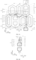
- FIG. 7 is a schematic diagram of a display device according to an embodiment of the present disclosure.
- the display device 800 includes the display substrate 100 of any one of the above. Therefore, the display device has beneficial effects corresponding to the beneficial effects of the display substrate, for example, the display device has higher light transmittance.
- the display device can improve the stability and service life of the compensation thin film transistor, thereby improving the long-term light-emitting stability and service life of the display substrate.
- the display device can be electronic products with display functions such as televisions, computers, notebook computers, flat computers, mobile phones, navigators, and electronic photo frames, etc.
Landscapes
- Engineering & Computer Science (AREA)
- Microelectronics & Electronic Packaging (AREA)
- Physics & Mathematics (AREA)
- General Physics & Mathematics (AREA)
- Theoretical Computer Science (AREA)
- Optics & Photonics (AREA)
- Computer Hardware Design (AREA)
- Electroluminescent Light Sources (AREA)
- Devices For Indicating Variable Information By Combining Individual Elements (AREA)
Applications Claiming Priority (2)
| Application Number | Priority Date | Filing Date | Title |
|---|---|---|---|
| PCT/CN2020/086997 WO2021217295A1 (fr) | 2020-04-26 | 2020-04-26 | Substrat d'affichage et dispositif d'affichage |
| PCT/CN2020/114559 WO2021217993A1 (fr) | 2020-04-26 | 2020-09-10 | Substrat d'affichage et dispositif d'affichage |
Publications (2)
| Publication Number | Publication Date |
|---|---|
| EP4145519A1 true EP4145519A1 (fr) | 2023-03-08 |
| EP4145519A4 EP4145519A4 (fr) | 2023-10-18 |
Family
ID=78373223
Family Applications (2)
| Application Number | Title | Priority Date | Filing Date |
|---|---|---|---|
| EP20929680.5A Active EP4145526B1 (fr) | 2020-04-26 | 2020-04-26 | Substrat d'affichage et dispositif d'affichage |
| EP20904234.0A Pending EP4145519A4 (fr) | 2020-04-26 | 2020-09-10 | Substrat d'affichage et dispositif d'affichage |
Family Applications Before (1)
| Application Number | Title | Priority Date | Filing Date |
|---|---|---|---|
| EP20929680.5A Active EP4145526B1 (fr) | 2020-04-26 | 2020-04-26 | Substrat d'affichage et dispositif d'affichage |
Country Status (4)
| Country | Link |
|---|---|
| US (5) | US12101973B2 (fr) |
| EP (2) | EP4145526B1 (fr) |
| CN (3) | CN120018704A (fr) |
| WO (3) | WO2021217295A1 (fr) |
Families Citing this family (18)
| Publication number | Priority date | Publication date | Assignee | Title |
|---|---|---|---|---|
| CN119894297B (zh) | 2020-04-26 | 2026-03-27 | 京东方科技集团股份有限公司 | 显示基板及显示装置 |
| US12101973B2 (en) | 2020-04-26 | 2024-09-24 | Chengdu Boe Optoelectronics Technology Co., Ltd. | Display substrate and display device |
| CN116998245A (zh) * | 2022-02-28 | 2023-11-03 | 京东方科技集团股份有限公司 | 显示面板、显示装置 |
| CN114709234B (zh) * | 2022-03-31 | 2025-12-19 | 上海天马微电子有限公司 | 一种显示面板及显示装置 |
| CN114784073B (zh) * | 2022-04-18 | 2024-11-12 | 京东方科技集团股份有限公司 | 显示面板和显示装置 |
| US20240349550A1 (en) * | 2022-05-26 | 2024-10-17 | Chengdu Boe Optoelectronics Technology Co., Ltd. | Display substrate and display apparatus |
| WO2023230870A1 (fr) * | 2022-05-31 | 2023-12-07 | 京东方科技集团股份有限公司 | Substrat d'affichage et appareil d'affichage |
| CN117501343A (zh) * | 2022-05-31 | 2024-02-02 | 京东方科技集团股份有限公司 | 显示基板及显示装置 |
| CN115312569B (zh) * | 2022-07-18 | 2025-12-19 | 京东方科技集团股份有限公司 | 显示基板及其制造方法、显示面板、显示装置 |
| WO2024031240A1 (fr) * | 2022-08-08 | 2024-02-15 | 京东方科技集团股份有限公司 | Substrat d'affichage, son procédé de fabrication et appareil d'affichage |
| US20250098468A1 (en) * | 2022-08-09 | 2025-03-20 | Chengdu Boe Optoelectronics Technology Co., Ltd. | Display Substrate, Preparation Method Therefor, and Display Apparatus |
| US12190822B2 (en) * | 2022-09-30 | 2025-01-07 | Chengdu Boe Optoelectronics Technology Co., Ltd. | Array substrate and display apparatus |
| KR20240055970A (ko) * | 2022-10-20 | 2024-04-30 | 삼성디스플레이 주식회사 | 표시 장치 |
| CN116096171A (zh) * | 2022-12-07 | 2023-05-09 | 武汉华星光电半导体显示技术有限公司 | 显示面板及显示装置 |
| CN115909944A (zh) * | 2022-12-27 | 2023-04-04 | 武汉天马微电子有限公司 | 显示面板及显示装置 |
| CN115915835A (zh) * | 2023-01-30 | 2023-04-04 | 合肥维信诺科技有限公司 | 显示面板及显示装置 |
| CN116234363B (zh) * | 2023-01-30 | 2026-04-03 | 合肥维信诺科技有限公司 | 显示面板及显示装置 |
| CN119072165A (zh) * | 2023-05-30 | 2024-12-03 | 京东方科技集团股份有限公司 | 显示面板及显示装置 |
Family Cites Families (40)
| Publication number | Priority date | Publication date | Assignee | Title |
|---|---|---|---|---|
| JP4310984B2 (ja) * | 2002-02-06 | 2009-08-12 | 株式会社日立製作所 | 有機発光表示装置 |
| KR102119159B1 (ko) | 2013-08-14 | 2020-06-05 | 삼성디스플레이 주식회사 | 유기 발광 표시 장치 |
| KR102182953B1 (ko) | 2013-11-26 | 2020-11-25 | 엘지디스플레이 주식회사 | 유기발광표시패널 및 이를 이용한 유기발광표시장치 |
| KR102360788B1 (ko) * | 2014-08-29 | 2022-02-11 | 엘지디스플레이 주식회사 | 박막 트랜지스터 기판 및 이를 이용한 표시장치 |
| JP6654280B2 (ja) * | 2015-01-14 | 2020-02-26 | 天馬微電子有限公司 | 画素アレイ及び電気光学装置並びに電気機器並びに画素アレイの駆動方法 |
| KR20160099979A (ko) * | 2015-02-13 | 2016-08-23 | 삼성디스플레이 주식회사 | 유기 발광 표시 장치 및 유기 발광 표시 장치의 제조 방법 |
| KR102381288B1 (ko) | 2015-03-04 | 2022-03-31 | 삼성디스플레이 주식회사 | 유기 발광 표시 장치 |
| KR102326806B1 (ko) | 2015-04-24 | 2021-11-15 | 엘지디스플레이 주식회사 | 서브 픽셀 배열 구조를 갖는 표시장치 |
| KR102415753B1 (ko) | 2015-05-04 | 2022-07-01 | 삼성디스플레이 주식회사 | 유기 발광 표시 장치 |
| US10381381B1 (en) * | 2015-10-20 | 2019-08-13 | Apple Inc. | Display with light transmitting windows |
| JP6855004B2 (ja) * | 2015-12-25 | 2021-04-07 | 天馬微電子有限公司 | 表示装置及び表示装置の製造方法 |
| JP2017146463A (ja) | 2016-02-17 | 2017-08-24 | 株式会社ジャパンディスプレイ | 表示装置 |
| CN110137214B (zh) | 2018-02-09 | 2024-08-09 | 京东方科技集团股份有限公司 | 显示基板和显示装置 |
| US10854684B2 (en) * | 2016-02-18 | 2020-12-01 | Boe Technology Group Co., Ltd. | Pixel arrangement structure and driving method thereof, display substrate and display device |
| US11264430B2 (en) | 2016-02-18 | 2022-03-01 | Chengdu Boe Optoelectronics Technology Co., Ltd. | Pixel arrangement structure with misaligned repeating units, display substrate, display apparatus and method of fabrication thereof |
| KR102825974B1 (ko) | 2016-09-13 | 2025-06-30 | 삼성디스플레이 주식회사 | 표시 장치 |
| US10802927B2 (en) * | 2016-11-17 | 2020-10-13 | Vmware, Inc. | System and method for checking and characterizing snapshot metadata using snapshot metadata database |
| CN111799319B (zh) | 2016-12-05 | 2022-12-13 | 群创光电股份有限公司 | 显示装置 |
| KR102758391B1 (ko) | 2016-12-30 | 2025-01-24 | 삼성디스플레이 주식회사 | 표시 장치 |
| CN106910765B (zh) * | 2017-05-04 | 2020-02-18 | 京东方科技集团股份有限公司 | 一种电致发光显示面板、其制作方法及显示装置 |
| KR20180131679A (ko) | 2017-05-30 | 2018-12-11 | 삼성디스플레이 주식회사 | 표시 장치 및 그 제조 방법 |
| JP6935055B2 (ja) * | 2017-07-21 | 2021-09-15 | 天馬微電子有限公司 | Oled表示装置、その回路、及びその製造方法 |
| CN109427851B (zh) | 2017-08-31 | 2021-04-23 | 昆山国显光电有限公司 | 像素结构、oled显示屏以及蒸镀掩膜版 |
| KR102660313B1 (ko) * | 2017-09-12 | 2024-04-25 | 엘지디스플레이 주식회사 | 전계 발광 표시장치 |
| KR102361370B1 (ko) * | 2017-10-13 | 2022-02-10 | 엘지디스플레이 주식회사 | 전계 발광 표시장치와 그 구동 방법 |
| KR102532307B1 (ko) | 2017-11-02 | 2023-05-15 | 삼성디스플레이 주식회사 | 표시장치 |
| CN110133885B (zh) | 2018-02-09 | 2024-08-02 | 京东方科技集团股份有限公司 | 像素排列结构、显示基板和显示装置 |
| CN109188805B (zh) * | 2018-09-14 | 2021-08-13 | 上海中航光电子有限公司 | 像素阵列结构、显示面板及显示装置 |
| US11387283B2 (en) * | 2018-09-28 | 2022-07-12 | Sharp Kabushiki Kaisha | Display device for reducing driving load of data lines |
| KR102593534B1 (ko) * | 2018-10-10 | 2023-10-25 | 삼성디스플레이 주식회사 | 디스플레이 장치 |
| CN109301088B (zh) | 2018-10-23 | 2020-11-24 | 昆山国显光电有限公司 | 一种有机发光显示面板及有机发光显示装置 |
| CN111490068B (zh) | 2019-01-29 | 2022-07-26 | 京东方科技集团股份有限公司 | 显示面板及其制造方法、显示装置 |
| CN110265442B (zh) * | 2019-06-14 | 2021-04-02 | 京东方科技集团股份有限公司 | 显示基板及包含其的显示面板 |
| CN110265458B (zh) * | 2019-06-27 | 2021-12-03 | 京东方科技集团股份有限公司 | 阵列基板及其制作方法、显示面板及显示装置 |
| CN110379366A (zh) * | 2019-07-29 | 2019-10-25 | 京东方科技集团股份有限公司 | 像素补偿复用电路、背板、显示面板及显示设备 |
| CN110491911A (zh) * | 2019-07-31 | 2019-11-22 | 云谷(固安)科技有限公司 | 像素排列结构和显示面板 |
| CN110444569A (zh) | 2019-08-02 | 2019-11-12 | 云谷(固安)科技有限公司 | 像素排列结构及显示面板 |
| CN110492018B (zh) * | 2019-08-09 | 2024-06-18 | 武汉华星光电半导体显示技术有限公司 | 一种显示装置 |
| CN111063711A (zh) * | 2019-12-10 | 2020-04-24 | 深圳市华星光电半导体显示技术有限公司 | 双面显示面板及其制备方法 |
| US12101973B2 (en) | 2020-04-26 | 2024-09-24 | Chengdu Boe Optoelectronics Technology Co., Ltd. | Display substrate and display device |
-
2020
- 2020-04-26 US US17/428,402 patent/US12101973B2/en active Active
- 2020-04-26 CN CN202510184614.8A patent/CN120018704A/zh active Pending
- 2020-04-26 EP EP20929680.5A patent/EP4145526B1/fr active Active
- 2020-04-26 WO PCT/CN2020/086997 patent/WO2021217295A1/fr not_active Ceased
- 2020-04-26 CN CN202080000606.9A patent/CN114097089B/zh active Active
- 2020-09-10 CN CN202080002061.5A patent/CN114097090B/zh active Active
- 2020-09-10 WO PCT/CN2020/114559 patent/WO2021217993A1/fr not_active Ceased
- 2020-09-10 EP EP20904234.0A patent/EP4145519A4/fr active Pending
- 2020-09-10 WO PCT/CN2020/114623 patent/WO2021217994A1/fr not_active Ceased
- 2020-09-10 US US17/299,565 patent/US11903274B2/en active Active
-
2023
- 2023-12-14 US US18/539,847 patent/US12232384B2/en active Active
-
2024
- 2024-06-12 US US18/741,382 patent/US20240334772A1/en active Pending
-
2025
- 2025-01-15 US US19/021,651 patent/US20250160158A1/en active Pending
Also Published As
| Publication number | Publication date |
|---|---|
| EP4145526A1 (fr) | 2023-03-08 |
| US20240334772A1 (en) | 2024-10-03 |
| CN114097090A (zh) | 2022-02-25 |
| WO2021217295A1 (fr) | 2021-11-04 |
| US11903274B2 (en) | 2024-02-13 |
| US20220320226A1 (en) | 2022-10-06 |
| WO2021217993A1 (fr) | 2021-11-04 |
| CN114097090B (zh) | 2025-05-23 |
| US20250160158A1 (en) | 2025-05-15 |
| EP4145519A4 (fr) | 2023-10-18 |
| US20220320247A1 (en) | 2022-10-06 |
| US12232384B2 (en) | 2025-02-18 |
| EP4145526B1 (fr) | 2026-03-18 |
| CN114097089A (zh) | 2022-02-25 |
| US20240114736A1 (en) | 2024-04-04 |
| US12101973B2 (en) | 2024-09-24 |
| EP4145526A4 (fr) | 2023-08-23 |
| CN114097089B (zh) | 2025-07-15 |
| CN120018704A (zh) | 2025-05-16 |
| WO2021217994A1 (fr) | 2021-11-04 |
Similar Documents
| Publication | Publication Date | Title |
|---|---|---|
| US12232384B2 (en) | Display substrate and display device | |
| US11678546B2 (en) | Array substrate with sub-pixels including power-supplying wire portions having openings therebetween and manufacturing method thereof, and display panel | |
| US20250063912A1 (en) | Display Substrate and Manufacturing Method Therefor, and Display Apparatus | |
| US11961471B2 (en) | Display substrate and display device | |
| CN112967682B (zh) | 一种显示面板及显示装置 | |
| EP4113496A1 (fr) | Substrat à réseau, panneau d'affichage et dispositif d'affichage | |
| US20240153461A1 (en) | Display Apparatus with Compensation and Driving Method therefor | |
| US12230215B2 (en) | Display substrate, manufacturing method therefor, and display apparatus | |
| CN115066755A (zh) | 显示基板及显示装置 | |
| CN114783372B (zh) | 像素驱动电路、显示面板及显示装置 | |
| KR20250054024A (ko) | 디스플레이 기판 및 디스플레이 장치 | |
| CN110890408A (zh) | 一种显示面板、显示装置 | |
| US12315442B2 (en) | Display device and driving method therefor | |
| US12518698B2 (en) | Display substrate, pixel circuit, driving method and display apparatus | |
| US12581995B2 (en) | Light emitting display panel | |
| US20250017089A1 (en) | Display Panel, Manufacturing Method Therefor, and Display Device | |
| CN118411931A (zh) | 一种显示面板及显示装置 | |
| WO2022226994A1 (fr) | Panneau d'affichage et dispositif d'affichage | |
| CN114842802B (zh) | 像素驱动电路、显示面板及显示装置 | |
| WO2023016335A1 (fr) | Substrat d'affichage et appareil d'affichage | |
| CN116648751A (zh) | 显示基板及其制备方法、显示装置 | |
| US11887543B1 (en) | Pixel drive circuit, display panel, and display device | |
| US12538675B2 (en) | Display panel and display apparatus | |
| US12125437B2 (en) | Display substrate and preparation method thereof, and display apparatus | |
| CN119947477A (zh) | 显示面板和显示装置 |
Legal Events
| Date | Code | Title | Description |
|---|---|---|---|
| STAA | Information on the status of an ep patent application or granted ep patent |
Free format text: STATUS: UNKNOWN |
|
| STAA | Information on the status of an ep patent application or granted ep patent |
Free format text: STATUS: THE INTERNATIONAL PUBLICATION HAS BEEN MADE |
|
| PUAI | Public reference made under article 153(3) epc to a published international application that has entered the european phase |
Free format text: ORIGINAL CODE: 0009012 |
|
| STAA | Information on the status of an ep patent application or granted ep patent |
Free format text: STATUS: REQUEST FOR EXAMINATION WAS MADE |
|
| 17P | Request for examination filed |
Effective date: 20210628 |
|
| AK | Designated contracting states |
Kind code of ref document: A1 Designated state(s): AL AT BE BG CH CY CZ DE DK EE ES FI FR GB GR HR HU IE IS IT LI LT LU LV MC MK MT NL NO PL PT RO RS SE SI SK SM TR |
|
| DAV | Request for validation of the european patent (deleted) | ||
| DAX | Request for extension of the european patent (deleted) | ||
| REG | Reference to a national code |
Ref country code: DE Ref legal event code: R079 Free format text: PREVIOUS MAIN CLASS: H01L0027320000 Ipc: H10K0059126000 |
|
| A4 | Supplementary search report drawn up and despatched |
Effective date: 20230914 |
|
| RIC1 | Information provided on ipc code assigned before grant |
Ipc: H10K 59/131 20230101ALI20230908BHEP Ipc: G09G 3/3241 20160101ALI20230908BHEP Ipc: H01L 21/77 20170101ALI20230908BHEP Ipc: H10K 59/80 20230101ALI20230908BHEP Ipc: H10K 59/126 20230101AFI20230908BHEP |