EP4145520A1 - Module tactile, panneau d'affichage et dispositif d'affichage - Google Patents
Module tactile, panneau d'affichage et dispositif d'affichage Download PDFInfo
- Publication number
- EP4145520A1 EP4145520A1 EP20904259.7A EP20904259A EP4145520A1 EP 4145520 A1 EP4145520 A1 EP 4145520A1 EP 20904259 A EP20904259 A EP 20904259A EP 4145520 A1 EP4145520 A1 EP 4145520A1
- Authority
- EP
- European Patent Office
- Prior art keywords
- touch
- substrate
- dielectric layer
- display panel
- insulating dielectric
- Prior art date
- Legal status (The legal status is an assumption and is not a legal conclusion. Google has not performed a legal analysis and makes no representation as to the accuracy of the status listed.)
- Granted
Links
Images



Classifications
-
- G—PHYSICS
- G06—COMPUTING OR CALCULATING; COUNTING
- G06F—ELECTRIC DIGITAL DATA PROCESSING
- G06F3/00—Input arrangements for transferring data to be processed into a form capable of being handled by the computer; Output arrangements for transferring data from processing unit to output unit, e.g. interface arrangements
- G06F3/01—Input arrangements or combined input and output arrangements for interaction between user and computer
- G06F3/03—Arrangements for converting the position or the displacement of a member into a coded form
- G06F3/041—Digitisers, e.g. for touch screens or touch pads, characterised by the transducing means
- G06F3/044—Digitisers, e.g. for touch screens or touch pads, characterised by the transducing means by capacitive means
- G06F3/0448—Details of the electrode shape, e.g. for enhancing the detection of touches, for generating specific electric field shapes, for enhancing display quality
-
- G—PHYSICS
- G06—COMPUTING OR CALCULATING; COUNTING
- G06F—ELECTRIC DIGITAL DATA PROCESSING
- G06F3/00—Input arrangements for transferring data to be processed into a form capable of being handled by the computer; Output arrangements for transferring data from processing unit to output unit, e.g. interface arrangements
- G06F3/01—Input arrangements or combined input and output arrangements for interaction between user and computer
- G06F3/03—Arrangements for converting the position or the displacement of a member into a coded form
- G06F3/041—Digitisers, e.g. for touch screens or touch pads, characterised by the transducing means
- G06F3/0416—Control or interface arrangements specially adapted for digitisers
- G06F3/04164—Connections between sensors and controllers, e.g. routing lines between electrodes and connection pads
-
- G—PHYSICS
- G06—COMPUTING OR CALCULATING; COUNTING
- G06F—ELECTRIC DIGITAL DATA PROCESSING
- G06F3/00—Input arrangements for transferring data to be processed into a form capable of being handled by the computer; Output arrangements for transferring data from processing unit to output unit, e.g. interface arrangements
- G06F3/01—Input arrangements or combined input and output arrangements for interaction between user and computer
- G06F3/03—Arrangements for converting the position or the displacement of a member into a coded form
- G06F3/041—Digitisers, e.g. for touch screens or touch pads, characterised by the transducing means
- G06F3/044—Digitisers, e.g. for touch screens or touch pads, characterised by the transducing means by capacitive means
- G06F3/0443—Digitisers, e.g. for touch screens or touch pads, characterised by the transducing means by capacitive means using a single layer of sensing electrodes
-
- H—ELECTRICITY
- H10—SEMICONDUCTOR DEVICES; ELECTRIC SOLID-STATE DEVICES NOT OTHERWISE PROVIDED FOR
- H10K—ORGANIC ELECTRIC SOLID-STATE DEVICES
- H10K50/00—Organic light-emitting devices
- H10K50/80—Constructional details
- H10K50/805—Electrodes
-
- H—ELECTRICITY
- H10—SEMICONDUCTOR DEVICES; ELECTRIC SOLID-STATE DEVICES NOT OTHERWISE PROVIDED FOR
- H10K—ORGANIC ELECTRIC SOLID-STATE DEVICES
- H10K50/00—Organic light-emitting devices
- H10K50/80—Constructional details
- H10K50/84—Passivation; Containers; Encapsulations
- H10K50/844—Encapsulations
-
- H—ELECTRICITY
- H10—SEMICONDUCTOR DEVICES; ELECTRIC SOLID-STATE DEVICES NOT OTHERWISE PROVIDED FOR
- H10K—ORGANIC ELECTRIC SOLID-STATE DEVICES
- H10K59/00—Integrated devices, or assemblies of multiple devices, comprising at least one organic light-emitting element covered by group H10K50/00
- H10K59/10—OLED displays
- H10K59/12—Active-matrix OLED [AMOLED] displays
- H10K59/131—Interconnections, e.g. wiring lines or terminals
-
- H—ELECTRICITY
- H10—SEMICONDUCTOR DEVICES; ELECTRIC SOLID-STATE DEVICES NOT OTHERWISE PROVIDED FOR
- H10K—ORGANIC ELECTRIC SOLID-STATE DEVICES
- H10K59/00—Integrated devices, or assemblies of multiple devices, comprising at least one organic light-emitting element covered by group H10K50/00
- H10K59/40—OLEDs integrated with touch screens
-
- G—PHYSICS
- G06—COMPUTING OR CALCULATING; COUNTING
- G06F—ELECTRIC DIGITAL DATA PROCESSING
- G06F2203/00—Indexing scheme relating to G06F3/00 - G06F3/048
- G06F2203/041—Indexing scheme relating to G06F3/041 - G06F3/045
- G06F2203/04103—Manufacturing, i.e. details related to manufacturing processes specially suited for touch sensitive devices
-
- G—PHYSICS
- G06—COMPUTING OR CALCULATING; COUNTING
- G06F—ELECTRIC DIGITAL DATA PROCESSING
- G06F2203/00—Indexing scheme relating to G06F3/00 - G06F3/048
- G06F2203/041—Indexing scheme relating to G06F3/041 - G06F3/045
- G06F2203/04111—Cross over in capacitive digitiser, i.e. details of structures for connecting electrodes of the sensing pattern where the connections cross each other, e.g. bridge structures comprising an insulating layer, or vias through substrate
-
- G—PHYSICS
- G06—COMPUTING OR CALCULATING; COUNTING
- G06F—ELECTRIC DIGITAL DATA PROCESSING
- G06F3/00—Input arrangements for transferring data to be processed into a form capable of being handled by the computer; Output arrangements for transferring data from processing unit to output unit, e.g. interface arrangements
- G06F3/01—Input arrangements or combined input and output arrangements for interaction between user and computer
- G06F3/03—Arrangements for converting the position or the displacement of a member into a coded form
- G06F3/041—Digitisers, e.g. for touch screens or touch pads, characterised by the transducing means
- G06F3/044—Digitisers, e.g. for touch screens or touch pads, characterised by the transducing means by capacitive means
- G06F3/0446—Digitisers, e.g. for touch screens or touch pads, characterised by the transducing means by capacitive means using a grid-like structure of electrodes in at least two directions, e.g. using row and column electrodes
-
- H—ELECTRICITY
- H10—SEMICONDUCTOR DEVICES; ELECTRIC SOLID-STATE DEVICES NOT OTHERWISE PROVIDED FOR
- H10K—ORGANIC ELECTRIC SOLID-STATE DEVICES
- H10K59/00—Integrated devices, or assemblies of multiple devices, comprising at least one organic light-emitting element covered by group H10K50/00
- H10K59/10—OLED displays
- H10K59/12—Active-matrix OLED [AMOLED] displays
- H10K59/1201—Manufacture or treatment
Definitions
- the present disclosure relates to the field of touch technology, in particular to a touch module, a display panel and a display apparatus.
- the FMLOC touch technology (namely, the Y-octa technology, is a technology that forms Tx and Rx channels in the FMLOC technology by directly manufacturing Metal Mesh trace through processes on the display region of back panel circuit to achieve touch functions) also encounters such a problem.
- the FMLOC touch technology namely, the Y-octa technology, is a technology that forms Tx and Rx channels in the FMLOC technology by directly manufacturing Metal Mesh trace through processes on the display region of back panel circuit to achieve touch functions
- the FMLOC touch technology namely, the Y-octa technology, is a technology that forms Tx and Rx channels in the FMLOC technology by directly manufacturing Metal Mesh trace through processes on the display region of back panel circuit to achieve touch functions
- an object of the present disclosure is to provide a display panel.
- a touch electrode pattern of a touch module is not prone to break during folding and curling, so as to ensure good touch performances of the display apparatus.
- the present disclosure provides a display panel.
- the display panel includes a substrate, a driving circuit structure layer arranged on one surface of the substrate, a light-emitting layer arranged on a surface of the driving circuit layer away from the substrate, an encapsulation layer arranged on a surface of the light-emitting layer away from the substrate, an insulating dielectric layer, touch electrode patterns, and a plurality of touch signal lines distributed at intervals.
- the light-emitting layer includes a plurality of light-emitting regions and non-light-emitting regions between two adjacent light-emitting regions.
- the insulating dielectric layer is arranged on a surface of the encapsulation layer away from the substrate.
- the insulating dielectric layer is provided with a plurality of hollow patterns, and includes a touch region, a peripheral signal trace region around the touch region, and a frame region around the peripheral signal trace region.
- the touch electrode patterns are arranged on a surface of the insulating dielectric layer and in the touch region.
- the touch electrode patterns include a plurality of first touch electrodes distributed at intervals in a first direction, and a plurality of second touch electrodes distributed at intervals in a second direction, insulated and spaced apart from the first touch electrodes. The first direction intersects with the second direction.
- the plurality of touch signal lines are arranged on a surface of the insulating dielectric layer and in the peripheral signal trace region. The touch signal lines are electrically connected to the touch electrode patterns.
- the hollow patterns are arranged around the touch electrode patterns and/or the touch signal lines.
- An orthographic projection of at least part of the hollow patterns on the substrate does not overlap with orthographic projections of the touch electrode patterns, the touch signal lines and the light-emitting regions on the substrate.
- a plurality of hollow patterns are arranged in the insulating dielectric layer, so that the hollow patterns may effectively release the stress caused by curling and folding of the display panel or display screen with the touch module, thereby avoiding the breakage of the touch electrode patterns and the disconnection of the touch signal channels, namely effectively achieving the purpose of protecting the touch electrode patterns.
- the first touch electrodes and the second touch electrodes are arranged on the same surface of the insulating dielectric layer.
- the display panel further includes bridge electrodes arranged on another surface of the insulating dielectric layer away from the first touch electrodes.
- the first touch electrodes include a plurality of first touch sub-electrodes distributed at intervals along the second direction.
- the bridge electrodes are electrically connected to two adjacent first touch sub-electrodes through first via holes penetrating the insulating dielectric layer.
- the plurality of hollow patterns include a plurality of first strip-shaped grooves and/or a plurality of first via holes distributed at intervals.
- the first touch electrodes and the second touch electrodes both include a plurality of grid structures.
- the grid structures are polygonal, and an orthographic projection of the grid structures on the substrate does not overlap with the light-emitting regions.
- the hollow patterns are a plurality of first via holes distributed at intervals.
- the plurality of first via holes are substantially arranged along an edge of the grid structures.
- An orthographic projection of the plurality of first via holes on the substrate is located between an orthographic projection of the light-emitting regions on the substrate and an orthographic projection of the grid structures on the substrate.
- the first touch electrodes and the second touch electrodes both include a plurality of grid structures.
- the grid structures are polygonal, and the orthographic projection of the grid structures on the substrate does not overlap with the light-emitting regions.
- the hollow patterns are a plurality of first strip-shaped grooves substantially extending along at least one edge of the grid structures. At least part of an orthographic projection of the first strip-shaped grooves on the substrate is located between the orthographic projection of the light-emitting regions on the substrate and the orthographic projection of the grid structures on the substrate.
- each of the light-emitting regions is located in one of the grid structures.
- the first strip-shaped grooves intersect with the plurality of the grid structures. Two adjacent first strip-shaped grooves are respectively positioned on two sides opposite to each other of the light-emitting regions.
- the hollow patterns are further arranged on one side of the touch signal lines away from the touch region.
- the hollow patterns are a plurality of second strip-shaped grooves.
- the extending direction of the second strip-shaped grooves is parallel or perpendicular to extending direction of the touch signal lines.
- the touch signal lines include a first touch signal line arranged on one side of the insulating dielectric layer away from the substrate, and a second touch signal line arranged on one side of the insulating dielectric layer close to the substrate.
- the first touch signal line is electrically connected to the second touch signal line through a second via penetrating the insulating dielectric layer.
- depth of the hollow patterns is less than or equal to thickness of the insulating dielectric layer.
- At least part of the grid structures has second via holes penetrating the grid structures.
- the first via holes meet at least one of the following conditions: inner diameter of the first via holes being 3-5 microns; distance between two adjacent first via holes being 3-5 microns; distance between the first via holes and the first touch electrodes, and distance between the first via holes and the second touch electrodes being less than or equal to 5 microns respectively; distance between the first via holes and the touch signal lines being less than or equal to 5 microns.
- the first strip-shaped grooves meet at least one of the following conditions: width of the first strip-shaped grooves being 3-5 microns; distance between the first strip-shaped grooves and the first touch electrodes, and distance between the first strip-shaped grooves and the second touch electrodes being less than or equal to 5 microns respectively; distance between the first strip-shaped grooves and the touch signal lines being less than or equal to 5 microns.
- the width of the second strip-shaped grooves is 10-20 microns.
- the distance between two adjacent second strip-shaped grooves is 5-8 microns.
- the width of each of the grid structures is d
- the inner diameter of a second via hole is r
- d/4 ⁇ r ⁇ d/3 is d
- d is 10-15 microns, and the distance between two adjacent second via holes is 3-5 microns.
- the display panel includes a first electrode, a pixel defining layer, an organic light-emitting layer, and a second electrode.
- the pixel defining layer is arranged on a surface of the driving circuit structure layer, away from the substrate, and defines a plurality of pixel opening.
- the organic light-emitting layer is arranged in the plurality of pixel openings.
- the second electrode is arranged on one side of the organic light-emitting layer, away from the first electrodes
- An orthographic projection of the hollow patterns on the substrate is located within an orthographic projection of the pixel defining layer on the substrate.
- the present application provides a touch module.
- the touch module includes an insulating dielectric layer, and touch electrode patterns arranged on a surface of the insulating dielectric layer.
- the touch electrode patterns include a plurality of first touch electrodes distributed at intervals in a first direction, and a plurality of second touch electrodes distributed at intervals in a second direction, insulated and spaced apart from the first touch electrodes.
- the first direction intersects with the second direction.
- the first touch electrodes and the second touch electrodes both include a plurality of grid structures. At least a part of the grid structures have a plurality of second via holes penetrating the grid structures. Therefore, due to the arrangement of the second via holes, the stress caused by folding and curling of the touch electrode patterns may be directly released, so as to avoid the breakage of the touch electrode patterns and avoid affecting the signal transmission.
- the present application provides a touch module.
- the touch module includes an insulating dielectric layer with a plurality of hollow patterns, touch electrode patterns arranged on a surface of the insulating dielectric layer and in the touch region, and a plurality of touch signal lines distributed at intervals.
- the insulating dielectric layer includes a touch region, a peripheral signal trace region around the touch region, and a frame region around the peripheral signal trace region.
- the touch electrode patterns include a plurality of first touch electrodes distributed at intervals in a first direction, and a plurality of second touch electrodes distributed at intervals in a second direction, insulated and spaced apart from the first touch electrodes. The first direction intersects with the second direction.
- the touch signal lines are arranged on a surface of the insulating dielectric layer and in the peripheral signal trace region.
- the touch signal lines are electrically connected to the touch electrode patterns.
- the hollow patterns are arranged around the touch electrode patterns and/or the touch signal lines. At least part of the hollow patterns does not overlap with the touch electrode patterns and the touch signal lines.
- a plurality of hollow patterns are arranged in the insulating dielectric layer, so that during the processes of curling and folding of the display panel or display screen with the touch module, the hollow patterns may effectively allow the stress caused by curling and folding released, thereby avoiding the breakage of the touch electrode patterns and the disconnection of the touch signal channels, namely effectively achieving the purpose of protecting the touch electrode patterns.
- first and second are used for description purposes only, and cannot be construed as indicating or implying relative importance or implicitly indicating the quantity of technical features referred to.
- the features defined with “first” and “second” may include one or more of the features explicitly or implicitly.
- a plurality of means two or more.
- the present disclosure provides a display panel.
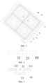
- FIG. 1 to FIG. 9 FIG. 3 , FIG. 6 and FIG. 7 are large version of the S region in FIG. 2 , in which the structure of the insulating dielectric layer in the touch region and peripheral signal trace region in FIG. 2 is not shown for ease of describing the touch electrode patterns; and
- FIG. 9 is a large version of the X region in FIG.
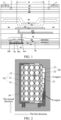
- the display panel includes a substrate 51; a driving circuit structure layer, arranged on one surface of the substrate 51; a light-emitting layer, arranged on a surface of the driving circuit layer away from the substrate 51 and includes a plurality of light-emitting regions AA and non-light-emitting regions BB between two adjacent light-emitting regions; an encapsulation layer, arranged on a surface of the light-emitting layer away from the substrate 51; an insulating dielectric layer 10, provided with a plurality of hollow patterns 11 (not shown in FIG.
- a touch electrode pattern 20 arranged on a surface of the insulating dielectric layer 10, located in the touch region 12, and including a plurality of first touch electrodes 21 distributed at intervals in a first direction, a plurality of second touch electrodes 22 distributed at intervals in a second direction, insulated and spaced apart from the first touch electrodes 21, herein, the first direction intersects with the second direction; and a plurality of touch signal lines 30, connected to the touch electrode patterns 20, distributed at intervals signal line arranged on a surface of the insulating dielectric layer 10 and located in the peripheral signal trace region 13.signal line.
- the hollow patterns 11 are arranged around the touch electrode patterns 20 and/or the touch signal lines 30.
- An orthographic projection of at least part of the hollow patterns 11 on the substrate 51 does not overlap with the orthographic projections of the touch electrode patterns 20, the touch signal lines 30 and the light-emitting regions AA on the substrate 10.
- a plurality of hollow patterns are arranged in the insulating dielectric layer, so that during the curling and folding processes of the display panel and display screen with the touch module, the hollow patterns may effectively allow the stress caused by the curling and folding released, thereby avoiding the breakage of the touch electrode patterns and/or the touch signal lines, and avoiding the disconnection of the touch signal channels, namely effectively achieving the purpose of protecting the touch electrode patterns and/or the touch signal lines.
- the hollow patterns may form a blocking force to further protect the touch electrode patterns and/or the touch signal lines.
- the display panel further includes a buffer layer 52 arranged between the substrate 51 and the driving circuit structure layer.
- the driving circuit structure layer includes, in the direction away from the substrate 51, an active layer 53, a first gate insulating layer 54, a gate electrode 541, a first interlayer dielectric layer 55, a first interlayer dielectric layer 56, a drain electrode 571, a source electrode 572, a second gate insulating layer 58, a first flat layer 59, a conductive connection layer 591 (the conductive connection layer is electrically connected to the drain electrode through a via hole), and a second flat layer 592, which are sequentially arranged.
- a display panel includes a first electrode 71, a pixel define layer 60 which is arranged on a surface of the driving circuit structure layer away from the substrate 51 (i. e., the surface of the second flat layer 592 away from the substrate) and defines a plurality of pixel openings 61, an organic light-emitting layer 72 arranged in the plurality of pixel openings 61, and a second electrode 73 arranged on a side of the organic light-emitting layer 72 away from the first electrode 71.
- An orthographic projection of the hollow patterns 11 on the substrate 10 is located within the orthographic projection of the pixel defining layer 60 on the substrate 10. Therefore, the FMLOC display screen with such a structure are provided with better folding and curling performances, and the touch electrode patterns are not prone to break.
- the specific structure of the touch module (including the insulating dielectric layer and the touch electrode patterns) is not particularly limited, thereby those skilled are provided flexibility of selection according to specific conditions.
- FIG. 5 is a cross-sectional diagram of the touch module at the bridge electrodes 23 in FIG. 2
- the first touch electrodes 21 include a plurality of first touch sub-electrodes 211 distributed at intervals along the second direction.
- the display panel further includes bridge electrodes 23 arranged on another surface of the insulating dielectric layer 10 away from the first touch electrodes 21, and electronically connected to two adjacent first touch sub-electrodes 211 through first vias penetrating the insulting dielectric layer 10.
- the first touch electrodes 21 and the second touch electrodes 22 are respectively arranged on two surfaces opposite to each other of the insulating dielectric layer 10, and in this case there is no need to arrange a bridge electrode.
- one of the first touch electrode 21 and the second touch electrode 22 serves as a driving electrode (Tx) and the other serves as a sensing electrode (Rx).
- the materials for forming the insulating dielectric layer include but are not limited to silicon nitride, silicon oxide, silicon oxynitride, and organic insulating materials, etc.
- the plurality of hollow patterns 11 include a plurality of first strip-shaped grooves 111 (as shown in FIG. 6 ) and/or a plurality of first via holes distributed at intervals (as shown in FIG. 2 ).
- both the first strip-shaped grooves 111 and the first via holes 112 may effectively make the stress caused by curling and folding released, and are also convenient for manufacturing and designing in terms of process.
- the hollow patterns are the first strip-shaped grooves
- the first strip-shaped grooves may make the stress released better.
- the specific shape of the first via holes may be any shape such as a circular shape, an oval shape, a rectangle shape, etc., which is not limited here.
- both the first touch electrodes 21 and the second touch electrodes 22 include a plurality of grid structures.
- the grid structures are polygonal (taking the quadrilateral shape as an example in FIG. 3 ), and an orthographic projection on the substrate does not overlap with the light-emitting regions AA.
- the hollow patterns 11 are a plurality of first via holes 112 distributed at intervals.
- the plurality of first via holes 112 are substantially arranged along the edge of the grid structures, and an orthographic projection of the first via holes 112 on the substrate 51 is located between an orthographic projection of the light-emitting regions AA on the substrate and an orthographic projection of the grid structures on the substrate 51.
- the arrangement of the first via holes does not negatively affect the light-emitting effect of the light-emitting regions and the image display of the display panel at the same time of making stress released.
- both the first touch electrodes 21 and the second touch electrodes 22 include a plurality of grid structures.
- the grid structures are polygonal (taking the quadrilateral shape as an example in FIG. 6 ), and an orthographic projection on the substrate does not overlap with the light-emitting regions AA.
- the hollow patterns 11 are a plurality of first strip-shaped grooves 111.
- the first strip-shaped grooves 111 extend along at least one edge of the grid structures substantially.
- At least part of the orthographic projection of the first strip-shaped grooves 111 on the substrate is located between an orthographic projection of the light-emitting regions AA on the substrate and an orthographic projection of the grid structures on the substrate.
- each of the light-emitting regions AA is located within one of the grid structures.
- the first strip-shaped grooves 111 intersect with a plurality of the grid structures.
- Two adjacent first strip-shaped grooves 111 i.e., two adjacent first strip-shaped grooves spanning the grid structures of the same column or row
- the stress may still be well released to protect the touch electrode patterns, without negatively affecting the light-emitting effect of the light-emitting regions and the image display of the display panel.
- the first via hole 112 meet at least one of the following conditions: the inner diameter D1 of a first via hole 112 being 3-5 microns (such as 3 microns, 3.5 microns, 4 microns, 4.5 microns or 5 microns); the distance D2 between two adjacent first via holes being 3-5 microns (such as 3 microns, 3.5 microns, 4 microns, 4.5 microns or 5 microns); the distances D3 between the first via holes 112 and the first touch electrodes 21, or between the first via holes 112 and the second touch electrodes 22 being less than or equal to 5 microns (for example, 5 microns, 4 microns, 3 microns, 2 microns, 1 micron or 0) respectively; the distance D4 between the first via hole 112 and the touch signal line 30 being less than or equal to 5 microns (such as 5 microns, 4 microns, 3 microns, 2 micro
- the first via holes 112 may allow the stress caused by folding and curling of the insulating dielectric layer, the touch electrode patterns and the touch signal lines released in a better way, without affecting the service performances of the touch module.
- the first strip-shaped grooves 111 meet at least one of the following conditions: the width D5 of a first strip-shaped groove 111 being 3-5 microns (such as 3 microns, 3.5 microns, 4 microns, 4.5 microns or 5 microns); the distances D6 between the first strip-shaped grooves 111 and the first touch electrodes 21, and between the first strip-shaped grooves 111 and the second touch electrodes 22 being less than or equal to 5 microns, respectively; the distance between the first strip-shaped grooves and the touch signal lines (not shown in the figure) being less than or equal to 5 microns (such as 5 microns, 4 microns, 3 microns, 2 microns, 1 micron or 0).
- the first strip-shaped grooves 111 may allow the stress caused by folding and curling of the insulating dielectric layer, the touch electrode patterns and the touch signal lines released in a better way, without affecting the service performances of the touch module.
- the distances D3 between the first via hole 112 (or the first strip-shaped groove 111) and the first touch electrodes 21, or between the first via hole 112 (or the first strip-shaped grooves 111) and the second touch electrodes 22 are less than or equal to 5 microns respectively, which means that the distance between the first via hole 112 (or the first strip-shaped groove 111) and the nearest first touch electrode forming the grid structures is less than or equal to 5 microns, and the distance between the first via hole 112 (or the first strip-shaped groove111) and the nearest second touch electrode forming the grid structures is less than or equal to 5 microns.
- the distance between the first via hole 112 (or the first strip-shaped groove 111) and the touch signal line 30 is less than or equal to 5 microns, which means that the distance between the first via hotel 12 (or the first strip-shaped groove 111) distributed on at least one side of the touch signal lines 30 in the direction along the width of the touch signal lines 30 and the touch signal lines 30 is less than or equal to 5 microns signal line.
- the hollow patterns 11 are further arranged on one side of the touch signal lines 30 away from the touch region 12 (i.e., the hollow patterns 11 are also arranged in the frame region 14 of the insulating dielectric layer 10). Therefore, arranging the hollow patterns in the frame region may further allow the stress caused by folding and curling of the insulating dielectric layer released, and thereby avoiding the adverse phenomenon of the touch electrode patterns and the touch signal lines breakage due to the unreleased stress of the insulating dielectric layer.
- the hollow patterns 11 in the frame region 14 are a plurality of second strip-shaped grooves 113.
- the extending direction of the plurality of second strip-shaped grooves 113 is parallel or perpendicular to the extending direction of the touch signal lines 30. Therefore, the second strip-shaped grooves 113 being parallel to the extending direction of the touch signal lines 30 may better prevent the touch electrode patterns and the touch signal lines from breaking due to the stress caused by folding of the display panel; the second strip-shaped groove 113 being perpendicular to the extending direction of the touch signal lines 30 may better allow the stress caused by folding released, thereby alleviating the breakage phenomenon of the touch electrode patterns and touch signal lines occurs due to being folded.
- the width D8 of the second strip-shaped grooves is 10-20 microns (such as 10 microns, 12 microns, 14 microns, 15 microns, 16 microns, 18 microns or 20 microns).
- the distance D7 between two adjacent second strip-shaped grooves is 5-8 microns (such as 5 microns, 6 microns, 7 microns, 8 microns or 9 microns). Therefore, the second strip-shaped grooves with the above size may effectively allow the stress caused by folding and curling of the insulating dielectric layer released, without affecting the service performances of the touch module.
- the width of the second strip-shaped grooves is less than 10 microns, the effect of stress release is relatively poor. If the width of the second strip-shaped groove is greater than 20 microns, the manufacturing cost of the second strip-shaped groove may be increased, and overall performances of the touch module may be negatively affected to some extent. If the distance D7 between two adjacent second strip-shaped grooves is less than 5 microns, the insulating dielectric layer between the adjacent second strip-shaped grooves is prone to break when the display screen is folded and curled, accordingly affecting the performances of the touch module.
- the distance D7 between two adjacent second strip-shaped grooves is larger than 8 microns, on the premise of a fixed frame region size, if the quantity of second strip-shaped grooves is less, the effect of stress release of the insulating dielectric layer will be relatively reduced then.
- the touch signal line 30 include a first touch signal line arranged on one side of the insulating dielectric layer 10 away from the substrate 51, and a second touch signal line arranged on one side of the insulating dielectric layer 10 close to the substrate 51.
- the first touch signal line is electrically connected to the second touch signal line through a second via penetrating the insulating dielectric layer.
- the first touch signal line is electrically connected to the first touch electrodes.
- the second touch signal line is electrically connected to the second touch electrodes.
- the first touch signal line is electrically connected to the second touch signal line through a second via penetrating through the insulating dielectric layer to achieve a parallel connection between the first touch signal line and the second touch signal line.
- hollow depth of the hollow patterns is less than or equal to thickness of the insulating dielectric layer. According to some embodiments of the present disclosure, hollow depth of the hollow patterns is equal to thickness of the insulating dielectric layer. That is, the hollow patterns penetrate the insulating dielectric layer. Therefore, the stress caused by curling and folding may be released in a better way.
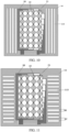
- the grid structures has second via holes 201 penetrating the grid structures (taking the grid structures formed by the first touch electrodes as an example in FIG. 12 ). Therefore, due to the arrangement of the second via holes 201, the stress caused by folding and curling of the touch electrode patterns 20 (i.e., the grid structures) may be directly released, so as to avoid the breakage of the touch electrode patterns 20 affecting the signal transmission.
- the width of each of the grid structures is d
- the inner diameter of a second via hole is r
- d/4 ⁇ r ⁇ d/3 the width of each of the grid structures.
- the second via holes with the above size may effectively allow the stress released without affecting the signal transmission of touch electrode patterns, ensure good impedance of the touch electrode patterns, and ensure that when being folded and curled, the touch electrode patterns may not break due to a larger inner diameter of the second via holes relative to the width of the touch electrode patterns.
- d is 10-15 microns (such as 10 microns, 11 microns, 12 microns, 13 microns, 14 microns or 15 microns).
- the second via holes with smaller inner diameter may be made in order to avoid that the width of part of the grid structures of the second via holes is not too small, thus the effect of stress release is relatively reduced; or alternatively, on the premise of making the second via holes with suitable inner diameter, the width of the corresponding grid structures of the second via holes may be too small, and the part with too small size of the grid structures may easily break when being folded or curled. If d is larger than 15 microns, the width of the grid structures is too large, which firstly wastes raw materials and increases the cost, and secondly affects the light transmittance of the display screen with the touch module.
- the distance S between two adjacent second via holes 201 is 3-5 microns (such as 3 microns, 3.5 microns, 4 microns, 4.5 microns or 5 microns). Therefore, the density of the second via holes is set appropriately, which may not only allow the stress caused by folding and curling of the touch electrode patterns released better, but also not affect the performances of the touch electrode patterns. If the distance S between two adjacent second via holes 201 is less than 3 microns, then the density of the second via holes is large, which may affect the service performances of the touch module. If the distance S between two adjacent second via holes 201 is larger than 5 microns, the effect of stress release may be reduced relatively.
- the present application provides a display apparatus.
- the display apparatus includes the aforementioned display panel. Therefore, when being folded or curled, the touch electrode patterns are not prone to break, which accordingly maintains good, sensitive and stable touch performances.
- the display apparatus is provided with all the features and advantages of the display panel and the touch module described above, which will not be described in detail here.
- the specific products of the above display apparatus do not need to meet specific requirement, and may be flexibly selected by those skilled in the art according to actual situations.
- the specific products of the above display apparatus include, but are not limited to, a mobile phone, a notebook, an iPad, a kindle, a game console or any other foldable display devices with display functions.
- the present application provides a touch module.
- the touch module includes an insulating dielectric layer 10, and touch electrode patterns 20 arranged on a surface of the insulating dielectric layer 10.
- the touch electrode patterns 10 include a plurality of first touch electrodes 21 distributed at intervals in a first direction, and a plurality of second touch electrodes 22 distributed at intervals in a second direction intersecting with the first direction and insulated and spaced apart from the first touch electrodes 21.
- the first touch electrodes 21 and the second touch electrodes 22 both include a plurality of grid structures. At least a part of the grid structures has a plurality of second via holes 201 penetrating the grid structures. Therefore, due to the arrangement of the second via holes 201, the stress caused by folding and curling of the touch electrode patterns 20 may be directly released, so as to avoid breaking when the display screen is folded or curled and affecting the signal transmission.
- the second via holes 201 are distributed in a row along the direction of the length extension of the grid structures.
- the specific structure of the touch module (including the insulating dielectric layer and the touch electrode patterns) is not particularly limited and may be flexibly selected by technicians according to specific conditions.
- FIG. 5 is a cross-sectional diagram of the touch module at the bridge electrodes 23 in FIG. 2
- the first touch electrodes 21 and the second touch electrodes 22 are arranged on the same surface of the insulating dielectric layer 10.
- the first touch electrodes 21 include a plurality of first touch sub-electrodes 211 distributed at intervals along the second direction.
- the touch module further includes bridge electrodes 23.
- the bridge electrodes 23 are arranged on another surface of the insulating dielectric layer 10 away from the first touch electrodes 21.
- the first touch electrodes 21 include a plurality of first touch sub-electrodes 211 distributed at intervals along the second direction.
- the bridge electrodes 23 are electronically connected to two adjacent first touch sub-electrodes 211 through first via holes penetrating the insulting dielectric layer 10.
- the first touch electrodes 21 and the second touch electrodes 22 are respectively arranged on two surfaces opposite to each other of the insulating dielectric layer 10, and in this case there is no need to arrange a bridge electrode.
- the width of each of the grid structures is d
- the inner diameter of a second via hole is r
- d/4 ⁇ r ⁇ d/3 the second via holes with the above size may effectively allow stress released without affecting the signal transmission of touch electrode patterns, ensuring good impedance of the touch electrode patterns, and simultaneously ensuring that when being folded and curled, the touch electrode patterns may not break due to a larger inner diameter of the second via holes relative to the width of the touch electrode patterns.
- d is 10-15 microns (such as 10 microns, 11 microns, 12 microns, 13 microns, 14 microns or 15 microns).
- the second via holes with smaller inner diameter may be made in order to avoid that the width of part of the grid structures of the second via holes is not too small, thus the effect of stress release is relatively reduced; or alternatively, on the premise of making the second via holes with suitable inner diameter, the width of the corresponding grid structures of the second via holes may be too small, and the part with a narrow size of the grid structures may easily break when being folded and curled. If d is larger than 15 microns, the width of the grid structures is too large, which wastes raw materials and increases the cost on the one hand, and affects the light transmittance of the display screen with the touch module on the other hand.
- the distance S between two adjacent second via holes 201 is 3-5 microns (such as 3 microns, 3.5 microns, 4 microns, 4.5 microns or 5 microns). Therefore, the density of the second via holes is set appropriately, which may not only allow stress caused by folding and curling of the grid structures released better, but also not affect the performances of the grid structures. If the distance S between two adjacent second via holes is less than 3 microns, the density of the second via holes is high, which may affect the service performances of the touch module. If the distance S between two adjacent second via holes is larger than 5 microns, the effect of stress release may be reduced relatively.
- the insulating dielectric layer in the touch module may be further provided with hollow patterns penetrating the insulating dielectric layer.
- the requirements for the hollow patterns are consistent with those for the hollow patterns in the aforementioned display panel, which will not be described in detail here.
- the stress caused by bending of the touch electrode patterns may be further relieved and released, which consequently avoid the breakage of the touch electrode patterns.
- the present application provides a touch module.
- the touch module includes an insulating dielectric layer 10 with a plurality of hollow patterns 11, touch electrode patterns 20, and a plurality of touch signal wires 30 distributed at intervals.
- the insulating dielectric layer 10 includes a touch region 12, a peripheral signal trace region 13 around the touch region 12, and a frame region 14 around the peripheral signal trace region 13.
- the plurality of touch electrode patterns 20 are arranged on a surface of the insulating dielectric layer 10 and located in the touch region 12.
- the touch electrode patterns include a plurality of first touch electrodes distributed at intervals in a first direction, and a plurality of second touch electrodes 22 distributed at intervals in a second direction intersecting with the first direction and insulated and spaced apart from the first touch electrodes 21.
- the touch signal lines 30 are arranged on a surface of the insulating dielectric layer 10 and located in the peripheral signal trace region 13.
- the touch signal lines 30 are electrically connected to the touch electrode patterns 20.
- the hollow patterns 11 are arranged around the touch electrode patterns 20 and/or the touch signal lines 30. At least part of the hollow patterns 11 does not overlap with the touch electrode patterns 20 and the touch signal lines 30.
- a plurality of hollow patterns are arranged in the insulating dielectric layer, so that during the curling and folding of the display panel or display screen with the touch module, the hollow patterns may effectively allow the stress caused by the curling and folding, thereby avoiding the breakage of the touch electrode patterns and the disconnection of the touch signal channels, namely effectively achieving the purpose of protecting the touch electrode patterns.
- the specific structure of the touch module (including the insulating dielectric layer and the touch electrode patterns) is not particularly limited and may be flexibly selected by technicians according to specific conditions.
- FIG. 5 is a cross-sectional diagram of the touch module at the bridge electrodes 23 in FIG. 2
- the first touch electrodes 21 and the second touch electrodes 22 are arranged on the same surface of the insulating dielectric layer 10.
- the first touch electrodes 21 include a plurality of first touch sub-electrodes 211 distributed at intervals along the second direction.
- the touch module further includes bridge electrodes 23.
- the bridge electrodes 23 are arranged on another surface of the insulating dielectric layer 10 away from the first touch electrodes 22.
- the first touch electrodes 21 include a plurality of first touch sub-electrodes 211 distributed at intervals along the second direction.
- the bridge electrodes 23 are electronically connected to two adjacent first touch sub-electrodes 211 through the first via holes penetrating the insulting dielectric layer 10.
- the first touch electrodes 21 and the second touch electrodes 22 are respectively arranged on two surfaces opposite to each other of the insulating dielectric layer 10, and in this case there is no need to arrange a bridge electrode.
- first touch electrode 21 and a second touch electrode 22 serves as a driving electrode (Tx) and the other serves as a sensing electrode (Rx).
- the plurality of hollow patterns 11 include a plurality of first strip-shaped grooves 111 (as shown in FIG. 6 ) and/or a plurality of first via holes distributed at intervals (as shown in FIG. 2 ).
- both the first strip-shaped grooves 111 and the first via holes 112 may effectively allow the stress caused by bending released, and are also convenient for manufacturing and designing in terms of process.
- the hollow patterns are the first strip-shaped grooves, if the extension direction along the length of the first strip-shaped grooves is consistent with the folding direction of the display panel, the first strip-shaped grooves may provide a better stress release.
- the specific shape of the first via holes may be any shape such as a circular shape, an oval shape, a rectangle shape, etc., which is not limited here.
- both the first touch electrodes 21 and the second touch electrodes 22 (taking the first touch electrodes 21 as an example in the figures) include a plurality of grid structures.
- the grid structures are polygonal (taking the quadrilateral shape as an example in FIG. 3 ), and an orthographic projection of which on the substrate does not overlap with the light-emitting regions AA.
- the hollow patterns 11 are a plurality of first via holes 112 distributed at intervals.
- the plurality of first via holes 112 are substantially arranged along the edge of the grid structures, and an orthographic projection of the plurality of first via holes 112 on the substrate 51 is located between an orthographic projection of the light-emitting regions AA on the substrate and an orthographic projection of the grid structures on the substrate 51.
- the arrangement of the first via holes will not negatively affect the light-emitting effect of the light-emitting regions and the image display of the display panel at the same time of achieving releasing stress.
- both the first touch electrodes 21 and the second touch electrodes 22 (taking the first touch electrodes 21 as an example in the figures) include a plurality of grid structures.
- the grid structures are polygonal (taking the quadrilateral shape as an example in FIG. 6 ), and an orthographic projection of which on the substrate does not overlap with the light-emitting regions AA.
- the hollow patterns 11 are a plurality of first strip-shaped grooves 111.
- the plurality of first strip-shaped grooves 111 are substantially arranged along at least one edge of the grid structures.
- At least part of the orthographic projection of the first strip-shaped grooves 111 on the substrate is located between an orthographic projection of the light-emitting regions AA on the substrate and an orthographic projection of the grid structures on the substrate.
- each of the light-emitting regions AA is located within one of the grid structures.
- the first strip-shaped grooves 111 intersect with a plurality of grid structures. Two adjacent first strip-shaped grooves 111 (i.e., two adjacent first strip-shaped grooves spanning the grid structures of the same column or same row) are respectively located on two sides opposite to each other of the light-emitting regions AA.
- the stress may still be well released to protect the touch electrode pattern, without negatively affecting the light-emitting effect of the light-emitting regions and the image display of the display panel.
- requirements for the size of the first via holes and the first strip-shaped grooves are consistent with those for the size of the first via holes and the first strip-shaped grooves in the aforementioned display panel, which will not be described in detail here.
- the hollow patterns 11 are further arranged on one side of the touch signal lines 30 away from the touch region 12 (i.e., the hollow patterns 11 are also arranged in the frame region 14 of the insulating dielectric layer 10). Therefore, the arrangement of the hollow patterns in the frame region may better allow the stress caused by folding and curling of the insulating dielectric layer released, and further avoids the adverse phenomenon of breakage of the touch electrode patterns and the touch signal lines due to the unreleased stress of the insulating dielectric layer.
- the hollow patterns 11 are a plurality of second strip-shaped grooves 113.
- the extending direction of the second strip-shaped grooves 113 is parallel or perpendicular to the extending direction of the touch signal lines 30. Therefore, the second strip-shaped groove 113 being parallel to the extending direction of the touch signal lines 30 may better prevent the touch electrode patterns and the touch signal lines from breaking due to the stress caused by folding of the display panel; the second strip-shaped groove 113 being perpendicular to the extending direction of the touch signal lines 30 may better allow the stress caused by folding released, thereby alleviating the phenomenon of breakage of the touch electrode patterns and touch signal lines because of folding.
- requirements for size of the second strip-shaped groove are consistent with those for size of the second strip-shaped groove in the aforementioned display panel, which will not be described in detail here.
- the present application provides a display apparatus.
- the display apparatus includes the aforementioned touch module. Therefore, when being folded or curled, the touch electrode patterns are not prone to break, which consequently remains good, sensitive and stable touch performances.
- the display apparatus is provided with all the features and advantages of the display panel and the touch module described above, which will not be described in detail here.
- the specific products of the above display apparatus are not particularly limited, and may be flexibly selected by those skilled in the art according to actual situations.
- the specific products of the above display apparatus include, but are not limited to, a mobile phone, a notebook, an iPad, a kindle, a game console and any other foldable display devices with display functions.
Landscapes
- Engineering & Computer Science (AREA)
- Theoretical Computer Science (AREA)
- General Engineering & Computer Science (AREA)
- Physics & Mathematics (AREA)
- Human Computer Interaction (AREA)
- General Physics & Mathematics (AREA)
- Computer Networks & Wireless Communication (AREA)
- Quality & Reliability (AREA)
- Optics & Photonics (AREA)
- Microelectronics & Electronic Packaging (AREA)
- Devices For Indicating Variable Information By Combining Individual Elements (AREA)
- Position Input By Displaying (AREA)
- Electroluminescent Light Sources (AREA)
Applications Claiming Priority (1)
| Application Number | Priority Date | Filing Date | Title |
|---|---|---|---|
| PCT/CN2020/088409 WO2021217614A1 (fr) | 2020-04-30 | 2020-04-30 | Module tactile, panneau d'affichage et dispositif d'affichage |
Publications (3)
| Publication Number | Publication Date |
|---|---|
| EP4145520A1 true EP4145520A1 (fr) | 2023-03-08 |
| EP4145520A4 EP4145520A4 (fr) | 2023-06-21 |
| EP4145520B1 EP4145520B1 (fr) | 2025-06-18 |
Family
ID=78331636
Family Applications (1)
| Application Number | Title | Priority Date | Filing Date |
|---|---|---|---|
| EP20904259.7A Active EP4145520B1 (fr) | 2020-04-30 | 2020-04-30 | Module tactile, panneau d'affichage et dispositif d'affichage |
Country Status (5)
| Country | Link |
|---|---|
| US (1) | US11609656B2 (fr) |
| EP (1) | EP4145520B1 (fr) |
| JP (1) | JP7555971B2 (fr) |
| CN (1) | CN114026694A (fr) |
| WO (1) | WO2021217614A1 (fr) |
Families Citing this family (12)
| Publication number | Priority date | Publication date | Assignee | Title |
|---|---|---|---|---|
| KR102870875B1 (ko) | 2020-09-04 | 2025-10-15 | 삼성디스플레이 주식회사 | 디지타이저 및 이를 포함한 전자 장치 |
| CN113687737B (zh) * | 2020-11-20 | 2024-07-19 | 合肥维信诺科技有限公司 | 触控面板、显示面板以及显示装置 |
| CN112905055B (zh) * | 2021-03-11 | 2024-07-02 | 京东方科技集团股份有限公司 | 显示基板及其制造方法、显示装置 |
| US11604548B2 (en) * | 2021-05-28 | 2023-03-14 | Microsoft Technology Licensing, Llc | Capacitive sensor mesh with discontinuities |
| US12229376B2 (en) | 2022-01-29 | 2025-02-18 | Chengdu Boe Optoelectronics Technology Co., Ltd. | Touch-control display panel, touch-control display apparatus and method for manufacturing touch-control layer |
| CN114779954B (zh) * | 2022-03-28 | 2025-03-25 | 京东方科技集团股份有限公司 | 一种触控面板和显示装置 |
| WO2023230967A1 (fr) | 2022-06-01 | 2023-12-07 | 京东方科技集团股份有限公司 | Écran d'affichage tactile et appareil d'affichage |
| US12481390B2 (en) * | 2022-06-24 | 2025-11-25 | Chengdu Boe Optoelectronics Technology Co., Ltd. | Touch display structure and display apparatus |
| JP2024033818A (ja) * | 2022-08-31 | 2024-03-13 | 富士フイルム株式会社 | 導電性フィルム、タッチセンサフィルム及び画像表示装置 |
| CN115424832B (zh) * | 2022-09-05 | 2025-09-12 | 京东方科技集团股份有限公司 | 线圈结构及电子设备 |
| CN115421618B (zh) * | 2022-11-04 | 2023-03-10 | 惠科股份有限公司 | 触控膜层和触控显示面板 |
| CN115963946A (zh) * | 2023-01-13 | 2023-04-14 | 昆山国显光电有限公司 | 触控显示面板和电子设备 |
Family Cites Families (16)
| Publication number | Priority date | Publication date | Assignee | Title |
|---|---|---|---|---|
| JP6698291B2 (ja) | 2014-08-13 | 2020-05-27 | 三星ディスプレイ株式會社Samsung Display Co.,Ltd. | タッチパネル及びこれを含む表示装置 |
| US9927939B2 (en) * | 2014-08-13 | 2018-03-27 | Samsung Display Co., Ltd. | Touch panel and display apparatus including the same |
| US10347702B2 (en) * | 2014-10-22 | 2019-07-09 | Lg Display Co., Ltd. | Flexible thin film transistor substrate and flexible organic light emitting display device |
| US10168844B2 (en) * | 2015-06-26 | 2019-01-01 | Samsung Display Co., Ltd. | Flexible display device |
| CN105742330A (zh) | 2016-03-16 | 2016-07-06 | 京东方科技集团股份有限公司 | 一种有机发光显示面板及其制作方法、显示装置 |
| CN106227380B (zh) | 2016-07-19 | 2019-07-02 | 上海天马微电子有限公司 | 一种触控传感器、柔性触控显示面板以及电子设备 |
| CN106952938B (zh) * | 2017-05-16 | 2020-06-02 | 上海天马微电子有限公司 | 一种柔性显示装置及其制造方法、以及柔性显示设备 |
| KR102325818B1 (ko) * | 2017-06-01 | 2021-11-12 | 엘지디스플레이 주식회사 | 터치 디스플레이 장치, 터치 디스플레이 패널 및 터치 디스플레이 패널의 제조 방법 |
| CN107315507B (zh) * | 2017-07-05 | 2020-06-30 | 京东方科技集团股份有限公司 | 一种柔性触控基板及其制备方法、触控显示装置 |
| CN109427818B (zh) * | 2017-08-31 | 2019-11-01 | 昆山国显光电有限公司 | 一种可折叠阵列基板和显示装置 |
| CN107977116B (zh) * | 2017-12-15 | 2020-02-07 | 武汉华星光电半导体显示技术有限公司 | 柔性触控面板、触控显示屏及触控显示装置 |
| CN108183121A (zh) | 2017-12-15 | 2018-06-19 | 武汉华星光电半导体显示技术有限公司 | 柔性显示面板及其制作方法 |
| KR102632590B1 (ko) * | 2018-10-16 | 2024-02-05 | 삼성디스플레이 주식회사 | 터치 센서 및 이를 포함한 표시 장치 |
| CN109460162B (zh) * | 2018-10-31 | 2022-05-24 | 上海天马微电子有限公司 | 一种触控显示面板以及电子设备 |
| CN209388283U (zh) * | 2019-01-08 | 2019-09-13 | 云谷(固安)科技有限公司 | 柔性触控显示面板及显示装置 |
| CN110568963B (zh) * | 2019-09-10 | 2023-10-24 | 京东方科技集团股份有限公司 | 一种显示面板、显示基板、显示装置 |
-
2020
- 2020-04-30 WO PCT/CN2020/088409 patent/WO2021217614A1/fr not_active Ceased
- 2020-04-30 CN CN202080000651.4A patent/CN114026694A/zh active Pending
- 2020-04-30 US US17/265,207 patent/US11609656B2/en active Active
- 2020-04-30 EP EP20904259.7A patent/EP4145520B1/fr active Active
- 2020-04-30 JP JP2021569529A patent/JP7555971B2/ja active Active
Also Published As
| Publication number | Publication date |
|---|---|
| JP2023531838A (ja) | 2023-07-26 |
| EP4145520B1 (fr) | 2025-06-18 |
| CN114026694A (zh) | 2022-02-08 |
| US20220113854A1 (en) | 2022-04-14 |
| US11609656B2 (en) | 2023-03-21 |
| WO2021217614A1 (fr) | 2021-11-04 |
| EP4145520A4 (fr) | 2023-06-21 |
| JP7555971B2 (ja) | 2024-09-25 |
Similar Documents
| Publication | Publication Date | Title |
|---|---|---|
| US11609656B2 (en) | Touch module, display panel and display apparatus | |
| US10529793B2 (en) | Display panel and display device | |
| US20250081797A1 (en) | Array substrate and display device | |
| CN110943114B (zh) | 一种可弯折显示面板及显示装置 | |
| CN106951125B (zh) | 一种触控显示面板及触控显示装置 | |
| CN110442259B (zh) | 触控基板及显示面板 | |
| CN104617106B (zh) | 一种阵列基板及显示装置 | |
| EP4057356B1 (fr) | Panneau d'affichage et appareil d'affichage | |
| WO2021190055A1 (fr) | Substrat d'affichage et son procédé de préparation, panneau d'affichage et dispositif d'affichage | |
| KR20120078293A (ko) | 트랜지스터와 그 제조방법 및 트랜지스터를 포함하는 전자소자 | |
| CN113809133B (zh) | 显示面板及显示装置 | |
| US11925061B2 (en) | Flexible display panel and electronic device | |
| US12236051B2 (en) | Touch module and display device | |
| CN111106153B (zh) | 一种显示面板、其制作方法及显示装置 | |
| CN110837321B (zh) | 显示面板及显示装置 | |
| CN110379841A (zh) | 一种显示面板及显示装置 | |
| US11847276B2 (en) | Touch substrate and touch display device | |
| CN113540124B (zh) | 一种阵列基板、显示面板及显示装置 | |
| CN116137119A (zh) | 显示面板及显示装置 | |
| US11169406B2 (en) | Touch and display driver integrated assembly including protective layers, method of manufacturing the same, and electronic apparatus | |
| CN114816122B (zh) | 一种触控显示面板和显示装置 | |
| CN115185120B (zh) | 一种显示面板、显示装置 | |
| CN112241223B (zh) | 显示屏及电子设备 | |
| WO2023184244A1 (fr) | Substrat d'affichage et dispositif d'affichage | |
| CN108847414B (zh) | 显示面板及显示装置 |
Legal Events
| Date | Code | Title | Description |
|---|---|---|---|
| STAA | Information on the status of an ep patent application or granted ep patent |
Free format text: STATUS: UNKNOWN |
|
| STAA | Information on the status of an ep patent application or granted ep patent |
Free format text: STATUS: THE INTERNATIONAL PUBLICATION HAS BEEN MADE |
|
| PUAI | Public reference made under article 153(3) epc to a published international application that has entered the european phase |
Free format text: ORIGINAL CODE: 0009012 |
|
| STAA | Information on the status of an ep patent application or granted ep patent |
Free format text: STATUS: REQUEST FOR EXAMINATION WAS MADE |
|
| 17P | Request for examination filed |
Effective date: 20210630 |
|
| AK | Designated contracting states |
Kind code of ref document: A1 Designated state(s): AL AT BE BG CH CY CZ DE DK EE ES FI FR GB GR HR HU IE IS IT LI LT LU LV MC MK MT NL NO PL PT RO RS SE SI SK SM TR |
|
| REG | Reference to a national code |
Ref country code: DE Ref legal event code: R079 Free format text: PREVIOUS MAIN CLASS: H01L0027320000 Ipc: H10K0059400000 Ref document number: 602020053094 Country of ref document: DE |
|
| A4 | Supplementary search report drawn up and despatched |
Effective date: 20230524 |
|
| RIC1 | Information provided on ipc code assigned before grant |
Ipc: G06F 3/041 20060101ALI20230517BHEP Ipc: H10K 59/40 20230101AFI20230517BHEP |
|
| DAV | Request for validation of the european patent (deleted) | ||
| DAX | Request for extension of the european patent (deleted) | ||
| GRAP | Despatch of communication of intention to grant a patent |
Free format text: ORIGINAL CODE: EPIDOSNIGR1 |
|
| STAA | Information on the status of an ep patent application or granted ep patent |
Free format text: STATUS: GRANT OF PATENT IS INTENDED |
|
| RIC1 | Information provided on ipc code assigned before grant |
Ipc: G06F 3/041 20060101ALI20250214BHEP Ipc: G06F 3/044 20060101ALI20250214BHEP Ipc: H10K 59/131 20230101ALI20250214BHEP Ipc: H10K 59/40 20230101AFI20250214BHEP |
|
| INTG | Intention to grant announced |
Effective date: 20250226 |
|
| GRAS | Grant fee paid |
Free format text: ORIGINAL CODE: EPIDOSNIGR3 |
|
| GRAA | (expected) grant |
Free format text: ORIGINAL CODE: 0009210 |
|
| STAA | Information on the status of an ep patent application or granted ep patent |
Free format text: STATUS: THE PATENT HAS BEEN GRANTED |
|
| AK | Designated contracting states |
Kind code of ref document: B1 Designated state(s): AL AT BE BG CH CY CZ DE DK EE ES FI FR GB GR HR HU IE IS IT LI LT LU LV MC MK MT NL NO PL PT RO RS SE SI SK SM TR |
|
| REG | Reference to a national code |
Ref country code: GB Ref legal event code: FG4D |
|
| REG | Reference to a national code |
Ref country code: CH Ref legal event code: EP |
|
| REG | Reference to a national code |
Ref country code: DE Ref legal event code: R096 Ref document number: 602020053094 Country of ref document: DE |
|
| REG | Reference to a national code |
Ref country code: CH Ref legal event code: EP |
|
| REG | Reference to a national code |
Ref country code: IE Ref legal event code: FG4D |
|
| PG25 | Lapsed in a contracting state [announced via postgrant information from national office to epo] |
Ref country code: FI Free format text: LAPSE BECAUSE OF FAILURE TO SUBMIT A TRANSLATION OF THE DESCRIPTION OR TO PAY THE FEE WITHIN THE PRESCRIBED TIME-LIMIT Effective date: 20250618 |
|
| REG | Reference to a national code |
Ref country code: LT Ref legal event code: MG9D |
|
| PG25 | Lapsed in a contracting state [announced via postgrant information from national office to epo] |
Ref country code: GR Free format text: LAPSE BECAUSE OF FAILURE TO SUBMIT A TRANSLATION OF THE DESCRIPTION OR TO PAY THE FEE WITHIN THE PRESCRIBED TIME-LIMIT Effective date: 20250919 Ref country code: NO Free format text: LAPSE BECAUSE OF FAILURE TO SUBMIT A TRANSLATION OF THE DESCRIPTION OR TO PAY THE FEE WITHIN THE PRESCRIBED TIME-LIMIT Effective date: 20250918 |
|
| PG25 | Lapsed in a contracting state [announced via postgrant information from national office to epo] |
Ref country code: BG Free format text: LAPSE BECAUSE OF FAILURE TO SUBMIT A TRANSLATION OF THE DESCRIPTION OR TO PAY THE FEE WITHIN THE PRESCRIBED TIME-LIMIT Effective date: 20250618 |
|
| PG25 | Lapsed in a contracting state [announced via postgrant information from national office to epo] |
Ref country code: HR Free format text: LAPSE BECAUSE OF FAILURE TO SUBMIT A TRANSLATION OF THE DESCRIPTION OR TO PAY THE FEE WITHIN THE PRESCRIBED TIME-LIMIT Effective date: 20250618 |
|
| PG25 | Lapsed in a contracting state [announced via postgrant information from national office to epo] |
Ref country code: RS Free format text: LAPSE BECAUSE OF FAILURE TO SUBMIT A TRANSLATION OF THE DESCRIPTION OR TO PAY THE FEE WITHIN THE PRESCRIBED TIME-LIMIT Effective date: 20250918 |
|
| REG | Reference to a national code |
Ref country code: NL Ref legal event code: MP Effective date: 20250618 |
|
| PG25 | Lapsed in a contracting state [announced via postgrant information from national office to epo] |
Ref country code: LV Free format text: LAPSE BECAUSE OF FAILURE TO SUBMIT A TRANSLATION OF THE DESCRIPTION OR TO PAY THE FEE WITHIN THE PRESCRIBED TIME-LIMIT Effective date: 20250618 |
|
| PG25 | Lapsed in a contracting state [announced via postgrant information from national office to epo] |
Ref country code: NL Free format text: LAPSE BECAUSE OF FAILURE TO SUBMIT A TRANSLATION OF THE DESCRIPTION OR TO PAY THE FEE WITHIN THE PRESCRIBED TIME-LIMIT Effective date: 20250618 |
|
| PG25 | Lapsed in a contracting state [announced via postgrant information from national office to epo] |
Ref country code: PT Free format text: LAPSE BECAUSE OF FAILURE TO SUBMIT A TRANSLATION OF THE DESCRIPTION OR TO PAY THE FEE WITHIN THE PRESCRIBED TIME-LIMIT Effective date: 20251020 |
|
| REG | Reference to a national code |
Ref country code: AT Ref legal event code: MK05 Ref document number: 1805431 Country of ref document: AT Kind code of ref document: T Effective date: 20250618 |
|
| PG25 | Lapsed in a contracting state [announced via postgrant information from national office to epo] |
Ref country code: IS Free format text: LAPSE BECAUSE OF FAILURE TO SUBMIT A TRANSLATION OF THE DESCRIPTION OR TO PAY THE FEE WITHIN THE PRESCRIBED TIME-LIMIT Effective date: 20251018 |
|
| PG25 | Lapsed in a contracting state [announced via postgrant information from national office to epo] |
Ref country code: AT Free format text: LAPSE BECAUSE OF FAILURE TO SUBMIT A TRANSLATION OF THE DESCRIPTION OR TO PAY THE FEE WITHIN THE PRESCRIBED TIME-LIMIT Effective date: 20250618 Ref country code: SM Free format text: LAPSE BECAUSE OF FAILURE TO SUBMIT A TRANSLATION OF THE DESCRIPTION OR TO PAY THE FEE WITHIN THE PRESCRIBED TIME-LIMIT Effective date: 20250618 |
|
| PG25 | Lapsed in a contracting state [announced via postgrant information from national office to epo] |
Ref country code: CZ Free format text: LAPSE BECAUSE OF FAILURE TO SUBMIT A TRANSLATION OF THE DESCRIPTION OR TO PAY THE FEE WITHIN THE PRESCRIBED TIME-LIMIT Effective date: 20250618 |
|
| PG25 | Lapsed in a contracting state [announced via postgrant information from national office to epo] |
Ref country code: PL Free format text: LAPSE BECAUSE OF FAILURE TO SUBMIT A TRANSLATION OF THE DESCRIPTION OR TO PAY THE FEE WITHIN THE PRESCRIBED TIME-LIMIT Effective date: 20250618 |
|
| PG25 | Lapsed in a contracting state [announced via postgrant information from national office to epo] |
Ref country code: EE Free format text: LAPSE BECAUSE OF FAILURE TO SUBMIT A TRANSLATION OF THE DESCRIPTION OR TO PAY THE FEE WITHIN THE PRESCRIBED TIME-LIMIT Effective date: 20250618 |
|
| PG25 | Lapsed in a contracting state [announced via postgrant information from national office to epo] |
Ref country code: SK Free format text: LAPSE BECAUSE OF FAILURE TO SUBMIT A TRANSLATION OF THE DESCRIPTION OR TO PAY THE FEE WITHIN THE PRESCRIBED TIME-LIMIT Effective date: 20250618 |
|
| PG25 | Lapsed in a contracting state [announced via postgrant information from national office to epo] |
Ref country code: ES Free format text: LAPSE BECAUSE OF FAILURE TO SUBMIT A TRANSLATION OF THE DESCRIPTION OR TO PAY THE FEE WITHIN THE PRESCRIBED TIME-LIMIT Effective date: 20250618 |
|
| PGFP | Annual fee paid to national office [announced via postgrant information from national office to epo] |
Ref country code: GB Payment date: 20260323 Year of fee payment: 7 |
|
| PG25 | Lapsed in a contracting state [announced via postgrant information from national office to epo] |
Ref country code: DK Free format text: LAPSE BECAUSE OF FAILURE TO SUBMIT A TRANSLATION OF THE DESCRIPTION OR TO PAY THE FEE WITHIN THE PRESCRIBED TIME-LIMIT Effective date: 20250618 |
|
| PG25 | Lapsed in a contracting state [announced via postgrant information from national office to epo] |
Ref country code: IT Free format text: LAPSE BECAUSE OF FAILURE TO SUBMIT A TRANSLATION OF THE DESCRIPTION OR TO PAY THE FEE WITHIN THE PRESCRIBED TIME-LIMIT Effective date: 20250618 |
|
| PLBE | No opposition filed within time limit |
Free format text: ORIGINAL CODE: 0009261 |
|
| STAA | Information on the status of an ep patent application or granted ep patent |
Free format text: STATUS: NO OPPOSITION FILED WITHIN TIME LIMIT |
|
| REG | Reference to a national code |
Ref country code: CH Ref legal event code: L10 Free format text: ST27 STATUS EVENT CODE: U-0-0-L10-L00 (AS PROVIDED BY THE NATIONAL OFFICE) Effective date: 20260430 |