EP4148997A1 - Volumenschallwellenresonator, filter, elektronische vorrichtung und verfahren zur einstellung eines elektromechanischen kopplungskoeffizienten - Google Patents
Volumenschallwellenresonator, filter, elektronische vorrichtung und verfahren zur einstellung eines elektromechanischen kopplungskoeffizienten Download PDFInfo
- Publication number
- EP4148997A1 EP4148997A1 EP21800399.4A EP21800399A EP4148997A1 EP 4148997 A1 EP4148997 A1 EP 4148997A1 EP 21800399 A EP21800399 A EP 21800399A EP 4148997 A1 EP4148997 A1 EP 4148997A1
- Authority
- EP
- European Patent Office
- Prior art keywords
- frame
- edges
- electrode
- layer
- frame edges
- Prior art date
- Legal status (The legal status is an assumption and is not a legal conclusion. Google has not performed a legal analysis and makes no representation as to the accuracy of the status listed.)
- Pending
Links
Images


Classifications
-
- H—ELECTRICITY
- H03—ELECTRONIC CIRCUITRY
- H03H—IMPEDANCE NETWORKS, e.g. RESONANT CIRCUITS; RESONATORS
- H03H9/00—Networks comprising electromechanical or electro-acoustic elements; Electromechanical resonators
- H03H9/02—Details
-
- H—ELECTRICITY
- H03—ELECTRONIC CIRCUITRY
- H03H—IMPEDANCE NETWORKS, e.g. RESONANT CIRCUITS; RESONATORS
- H03H9/00—Networks comprising electromechanical or electro-acoustic elements; Electromechanical resonators
- H03H9/02—Details
- H03H9/02007—Details of bulk acoustic wave devices
- H03H9/02086—Means for compensation or elimination of undesirable effects
- H03H9/02118—Means for compensation or elimination of undesirable effects of lateral leakage between adjacent resonators
-
- H—ELECTRICITY
- H03—ELECTRONIC CIRCUITRY
- H03H—IMPEDANCE NETWORKS, e.g. RESONANT CIRCUITS; RESONATORS
- H03H9/00—Networks comprising electromechanical or electro-acoustic elements; Electromechanical resonators
- H03H9/02—Details
- H03H9/02007—Details of bulk acoustic wave devices
-
- H—ELECTRICITY
- H03—ELECTRONIC CIRCUITRY
- H03H—IMPEDANCE NETWORKS, e.g. RESONANT CIRCUITS; RESONATORS
- H03H9/00—Networks comprising electromechanical or electro-acoustic elements; Electromechanical resonators
- H03H9/02—Details
- H03H9/05—Holders or supports
-
- H—ELECTRICITY
- H03—ELECTRONIC CIRCUITRY
- H03H—IMPEDANCE NETWORKS, e.g. RESONANT CIRCUITS; RESONATORS
- H03H9/00—Networks comprising electromechanical or electro-acoustic elements; Electromechanical resonators
- H03H9/02—Details
- H03H9/125—Driving means, e.g. electrodes, coils
- H03H9/13—Driving means, e.g. electrodes, coils for networks consisting of piezoelectric or electrostrictive materials
- H03H9/131—Driving means, e.g. electrodes, coils for networks consisting of piezoelectric or electrostrictive materials consisting of a multilayered structure
-
- H—ELECTRICITY
- H03—ELECTRONIC CIRCUITRY
- H03H—IMPEDANCE NETWORKS, e.g. RESONANT CIRCUITS; RESONATORS
- H03H9/00—Networks comprising electromechanical or electro-acoustic elements; Electromechanical resonators
- H03H9/02—Details
- H03H9/125—Driving means, e.g. electrodes, coils
- H03H9/13—Driving means, e.g. electrodes, coils for networks consisting of piezoelectric or electrostrictive materials
- H03H9/132—Driving means, e.g. electrodes, coils for networks consisting of piezoelectric or electrostrictive materials characterized by a particular shape
-
- H—ELECTRICITY
- H03—ELECTRONIC CIRCUITRY
- H03H—IMPEDANCE NETWORKS, e.g. RESONANT CIRCUITS; RESONATORS
- H03H9/00—Networks comprising electromechanical or electro-acoustic elements; Electromechanical resonators
- H03H9/15—Constructional features of resonators consisting of piezoelectric or electrostrictive material
- H03H9/17—Constructional features of resonators consisting of piezoelectric or electrostrictive material having a single resonator
- H03H9/171—Constructional features of resonators consisting of piezoelectric or electrostrictive material having a single resonator implemented with thin-film techniques, i.e. of the film bulk acoustic resonator [FBAR] type
- H03H9/172—Means for mounting on a substrate, i.e. means constituting the material interface confining the waves to a volume
- H03H9/173—Air-gaps
-
- H—ELECTRICITY
- H03—ELECTRONIC CIRCUITRY
- H03H—IMPEDANCE NETWORKS, e.g. RESONANT CIRCUITS; RESONATORS
- H03H9/00—Networks comprising electromechanical or electro-acoustic elements; Electromechanical resonators
- H03H9/46—Filters
- H03H9/54—Filters comprising resonators of piezoelectric or electrostrictive material
- H03H9/58—Multiple crystal filters
- H03H9/582—Multiple crystal filters implemented with thin-film techniques
- H03H9/586—Means for mounting to a substrate, i.e. means constituting the material interface confining the waves to a volume
- H03H9/587—Air-gaps
-
- H—ELECTRICITY
- H03—ELECTRONIC CIRCUITRY
- H03H—IMPEDANCE NETWORKS, e.g. RESONANT CIRCUITS; RESONATORS
- H03H9/00—Networks comprising electromechanical or electro-acoustic elements; Electromechanical resonators
- H03H9/46—Filters
- H03H9/54—Filters comprising resonators of piezoelectric or electrostrictive material
- H03H9/58—Multiple crystal filters
- H03H9/60—Electric coupling means therefor
- H03H9/605—Electric coupling means therefor consisting of a ladder configuration
Definitions
- Embodiments of the present disclosure relate to the field of semiconductors, and in particular, to a bulk acoustic wave resonator method, a filter having the resonator, a method of adjusting an electromechanical coupling coefficient of the bulk acoustic wave resonator, and an electronic device having the filter or the resonator.
- a bulk acoustic wave filter has the advantages of low insertion loss, high rectangular coefficient, high power capacity and the like, and thus is widely applied to the current wireless communication system and is an important component for determining the quality of a radio-frequency signal for entering and exiting the communication system.
- each resonator needs to have different performance, therefore how to accurately regulate and control the performance of each resonator that forms the bulk acoustic wave filter is the direction of the subsequent key research for the bulk acoustic wave filter.
- the filter is composed of resonators with two functions, that is, series connection and parallel connection.
- the performance difference therebetween is not significant, which is unfavorable to improving the performance of the filter.
- An electromechanical coupling coefficient (kt 2 ) for the same frequency on the same substrate is not adjustable, and if the frequency of the resonator is determined, the electromechanical coupling coefficient of the resonator is generally determined.
- the current development demand requires resonators with different electromechanical coupling coefficients under the same frequency or specific frequency difference.
- resonators with the same frequency and different electromechanical coupling coefficients need to be used in practice.
- the present disclosure provides a new structural solution to improve the degree of freedom of an electromechanical coupling coefficient of a bulk acoustic wave resonator, such that the performance of a filter can be further improved.
- a bulk acoustic wave resonator includes a substrate, an acoustic mirror, a bottom electrode, a top electrode, and a piezoelectric layer.
- the top electrode is provided with bulge portions at both a top-electrode connection end and a non-top-electrode connection end, and top surfaces of the bulge portions are higher than a top surface of an inner side portion of the top electrode.
- the inner side portion is a convex polygonal region having edges, the bulge portions are arranged around the convex polygonal region to form an electrode frame with a polygonal shape, and the electrode frame includes a plurality of frame edges. The plurality of frame edges of the electrode frame has lateral width change within the acoustic mirror.
- the embodiments of the present disclosure further relate to a method of adjusting an electromechanical coupling coefficient of the above bulk acoustic wave resonator.
- the method includes a step of adjusting the electromechanical coupling coefficient by adjusting the widths of the plurality of frame edges of the electrode frame within the acoustic mirror in the lateral direction.
- the method further includes a step of adjusting the electromechanical coupling coefficient by selecting a ratio of a number of frame edges of the plurality of frame edges that have adjusted widths to a total number of the plurality of frame edges of the electrode frame.
- the embodiments of the present disclosure further relate to a filter.
- the filter includes a series branch including a plurality of series resonators and a plurality of parallel branch, and each of the plurality of parallel branches includes a parallel resonator.
- At least one resonator of the parallel resonators and the plurality of series resonators has an electromechanical coupling coefficient that is different from electromechanical coupling coefficients of other resonators of the parallel resonators and the plurality of series resonators, and the at least one resonator is the above bulk acoustic wave resonator.
- the embodiments of the present disclosure further relate to an electronic device including the above filter or the resonator.
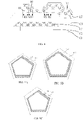
- FIG. 1 is a top view of a bulk acoustic wave resonator according to an exemplary embodiment of the present disclosure
- FIG. 2 is a schematic sectional view along line 1A-1A in FIG. 1
- FIG. 3A is a cross-sectional view for exemplarily illustrating an insertion layer in FIG. 1A.
- an effective region of the resonator has a convex pentagonal structure, but the present disclosure is not limited thereto and may be other convex polygonal structures.
- the resonator is only provided with a protrusion structure 105, but is not provided with an air gap structure (as shown later in FIG. 6 ).
- the protrusion structure 105 may have different widths on different edges of a pentagon, d21 and d22 in FIG. 2 .
- the width of an edge is a width within a boundary of an acoustic mirror along a lateral direction or radial direction of the resonator. That is, the width of the protrusion structure on each edge of the pentagon is different, and the difference in width herein means that the width of at least one edge is different from the widths of the remaining edges.
- An electromechanical coupling coefficient of the resonator can be adjusted by changing the width of the protrusion structure 105 on each edge and the proportion of each width for the five edges (i.e., the ratio of the number of edges with adjusted widths to the total number of edges of the polygon). Further, each edge is provided with the protrusion structure, such that the parallel impedance Rp (or a quality factor Qp) at a parallel resonance frequency may be kept at a relatively high level without a significant drop that may be caused by the adjustment of the width of the protrusion structure on each edge.
- the top electrode 107 is provided with bulge portions both at a top-electrode connection end (right side in FIG. 2 ) and a non-top-electrode connection end (left side in FIG. 2 ). It is evident from the figure that the bulge portion includes the wing structure 113 and a part of the bridge structure 114 in FIG. 6 . In FIG. 2 , a top surface of the bulge portion is higher than a top surface of an inner side portion M of the top electrode. As shown in FIG.
- the inner side portion M of the top electrode is a convex polygonal region having five edges, the bulge portion is arranged around the convex polygonal region to form a polygonal electrode frame, and the electrode frame includes a plurality of frame edges.
- the electrode frame is formed of the wing structure 113 and the bridge structure 114 that is located on an inner side of an acoustic mirror.
- the protrusion structure 105 is arranged below the electrode frame.
- the widths of the protrusion structures have a corresponding relationship with the electromechanical coupling coefficient kt 2 of the resonator.
- the electromechanical coupling coefficients of resonators with the same area decrease as the widths of the protrusion structures increase.
- the plurality of frame edges of the electrode frame of the resonator has different widths.
- the widths of the electrode frame may be determined by the widths of the protrusion structures 105.
- the five edges of the protrusion structure 105 are configured to have different protrusion structure widths, such that kt 2 of the resonator can be adjusted and other properties (e.g., a Q value at a parallel resonator frequency) are substantially unaffected.
- kt 2 can be further adjusted by selecting the number of edges of the protrusion structure of each width. For example, when the widths of five edges of the protrusion structure are all 2 ⁇ m, kt 2 is 8.0%; when the widths of four edges of the protrusion structure are all 2 ⁇ m and the width of another edge is 5 ⁇ m, kt 2 is 7.9%; when the widths of three edges of the protrusion structure are all 2 ⁇ m and the widths of other two edges are 5 ⁇ m, kt 2 is 7.8%; when the widths of two edges of the protrusion structure are both 2 ⁇ m and the widths of other three edges are 5 ⁇ m, kt 2 is 7.7%; when the width of one edge of the protrusion structure is 2 ⁇ m and the widths of other four edges are 5 ⁇ m, kt 2 is 7.6%; and when the widths of five edges of the protrusion structure are all 5 ⁇ m, kt 2 is 7.5%.
- FIG. 12 is a change graph of parallel impedance (Rp) of a resonator that is provided with a conventional protrusion structure versus the widths W of the protrusion structure.
- the traditional protrusion structure refers to a case where widths of all edges of the protrusion structures in one resonator are the same.
- the value of the parallel impedance Rp exhibits periodic characteristics with the increase in the width W, and each period has a peak point.
- the widths a1, a2, a3, a4, a5, and the like of the protrusion structure corresponding to local peak values approximately satisfy a proportional relationship of a1: a2: a3: a4: a5:...
- the electromechanical coupling coefficient monotonically decreases along with the increase in the widths of the protrusion structure. Therefore, in order to adjust kt 2 of a resonator and ensure that the value of the parallel impedance Rp of the resonator substantially remains unchanged, the widths of the protrusion structure corresponding to the peak values in different periods may be combined. For example, as described above, the width of the protrusion structure corresponding to the peak value of the first period is 2 ⁇ m, and the width of the protrusion structure corresponding to the peak value of the second period is 5 ⁇ m. In this embodiment, the protrusion structures with such two widths are combined on one resonator, so that the parallel impedance Rp can be maintained at a peak value level on the basis of adjusting kt 2 .
- the electromechanical coupling coefficient of the resonator is freely adjusted in a range without influence on other performance.
- the resonator for forming the filter can satisfy the above requirements by setting specific thicknesses of the bottom electrode, the piezoelectric layer, and the top electrode and the electromechanical coupling coefficient thereof is thus substantially determined.
- the electromechanical coupling coefficients of different resonators are different from each other.
- the electromechanical coupling coefficient can be adjusted in a range by providing different protrusion structures on each edge of the resonator and configuring different widths of the wing and the bridge structure. Therefore, the electromechanical coupling coefficient is flexibly adjusted by selecting widths of two or more protrusion structures or widths of two or more wings or bridges on different edges of the resonator and controlling the proportion of each width to the five edges.
- the bottom electrode, the piezoelectric layer and the top electrode may determine great adjustment of the electromechanical coupling coefficient of the resonator, and the solution provided by the present disclosure may realize slight adjustment of the electromechanical coupling coefficient.
- the boundary of the protrusion structure 105 is linear.
- an inner side boundary and an outer side boundary of the protrusion structure 105 are both straight lines.
- the present disclosure is not limited thereto.
- the inner sides of two edges of the protrusion structure 105 have concave-convex shapes.
- the concave-convex shape herein includes the concave-convex shapes in the claims, which not only include a zigzag shape in which a convex cross section or concave cross-section is rectangular as shown in FIG. 3A , but also include other shapes in which the convex cross sections or concave cross sections are nonlinear.
- the concave-convex shape is arranged on the inner side of the protrusion structure, but the present disclosure is not limited thereto, and the concave-convex shape may be arranged on the outer side of the protrusion structure.
- concave-convex shapes may be arranged on the inner side and the outer side of one edge of the protrusion structure, or a concave-convex shape is arranged on the outer side of one edge and another concave-convex shape is arranged on the inner side of another edge.
- the width of the frame edge of the insertion frame is determined by a maximum width thereof.
- the protrusion structure 105 is an insertion layer, which is located between the top electrode and the piezoelectric layer.
- the insertion layer is arranged between the top electrode 107 and the piezoelectric layer 104.
- the bulge portion includes a bridge portion or bridge structure 114 at the top-electrode connection end and a wing portion or wing structure 113 at the non-top-electrode connection end.
- the insertion layer includes an insertion frame that corresponds to the protrusion structure 105 in FIG. 3A or 3B and is located in the acoustic mirror in the lateral direction.
- the insertion frame and the electrode frame have the same inner side boundary and outer side boundary in the lateral direction.
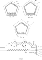
- FIG. 4 is a schematic sectional view of a bulk acoustic wave resonator according to an exemplary embodiment of the present disclosure, which is similarly taken along line 1A-1A in FIG. 1 .
- the cross section of the protrusion structure in FIG. 4 has a step shape.
- the protrusion structure includes a first protrusion structure 105 and a second protrusion structure 106.
- the first protrusion structure 105 is located on the outer side and the second protrusion structure 106 is located on the inner side.
- a side close to the center of the resonator in the lateral direction is an inner side
- a side away from the center of the resonator is an outer side.
- the first protrusion structure 105 and the second protrusion structure 106 form an insertion layer.
- the first protrusion structure 105 is a first insertion sub-layer
- the second protrusion structure 106 is a second insertion sub-layer.
- the frame edge of the insertion frame of the insertion layer which is located on the inner side of the boundary of the acoustic mirror, forms a step frame edge with a height increasing from the inner side to the outer side, and each insertion sub-layer forms a corresponding insertion sub-frame.
- FIGS. 5A-5C are respectively cross-sectional views for exemplarily illustrating the insertion layer in FIG. 4 , in which the frame edges of the insertion sub-frame are straight frame edges having straight inner side boundaries and straight outer side boundaries.
- FIGS. 5D-5F are respectively cross-sectional views for exemplarily illustrating the insertion layer in FIG. 4 .
- an inner side of a second insertion sub-frame corresponding to 106 has a concave-convex shape and a first insertion sub-frame corresponding to 105 has a straight edge, as shown in FIG. 5D .
- an outer side of the first insertion sub-frame corresponding to 105 has a concave-convex shape and the second insertion sub-frame corresponding to 106 has a straight edge, as shown in FIG. 5E .
- the outer side of the first insertion sub-frame corresponding to 105 has a concave-convex shape and the inner side of the second insertion sub-frame corresponding to 106 has a concave-convex shape, as shown in FIG. 5F .
- the present disclosure is not limited thereto, but includes the solution that an inner side boundary and/or an outer side boundary of at least one frame edge of at least one insertion sub-frame has a concave-convex shape.
- widths of the frame edges of the insertion frame may be configured in such a manner that, as shown in FIG. 5A , widths of the frame edges of the second insertion sub-frame corresponding to 106 are different (e.g., d31 is different from d32 in FIG. 4 ), and the widths of the frame edges of the first insertion sub-frame corresponding to 105 are the same.
- the widths of the frame edges of the insertion frame may be configured in such a manner that, as shown in FIG. 5B , the widths of the frame edges of the first insertion sub-frame corresponding to 105 are different (e.g., d21 is different from d22 in FIG.
- the widths of the frame edges of the insertion frame may be configured in such a manner that, as shown in FIG. 5C , the widths of the frame edges of the first insertion sub-frame are different, and the widths of the frame edges of the second insertion sub-frame are different.
- a total width of the frame edges of the insertion frame i.e. a sum of widths of the first insertion sub-frame and the second insertion sub-frame on the same frame edge, remains unchanged.
- a total width of the frame edges of the insertion frame changes.
- the insertion frame is formed by two insertion sub-frames, but the present disclosure is not limited thereto.
- the insertion frame may be formed by more insertion sub-frames connected to each other in the lateral direction.
- first insertion sub-frame and the second insertion sub-frame are shown separately in the lateral direction.
- the same thickness portions of the first insertion sub-frame and the second insertion sub-frame may be deposited and patterned, and a portion of the first insertion sub-frame within the same thickness portions, which is higher than the second insertion sub-frame, is then deposited and patterned.
- the insertion layer may not be made of a conductive material, and may be made of a non-conductive medium.
- FIG. 6 is a schematic sectional view of a bulk acoustic wave resonator according to an exemplary embodiment of the present disclosure, which is similarly taken along the line 1A-1A in FIG. 1 .
- an air gap 109 is arranged between a bulge portion of a top electrode and a top surface of a piezoelectric layer.
- FIG. 7A-7B are cross-sectional views for exemplarily illustrating an insertion layer in FIG. 6 , respectively.
- FIG. 7A illustrates change in widths of frame edges of an insertion frame formed by the air gap 109.
- FIG. 7B illustrates change in the widths of the frame edges of the insertion frame formed by the air gap 109 and concave-convex shapes of the boundaries of the frame edges.
- the description of the change in the width of the metal insertion frame as shown in FIG. 3 is also applicable to the air gap insertion frame in FIG. 7B .
- the non-conductive medium may be, for example, aluminum nitride, silicon dioxide, and silicon nitride.
- FIG. 8 is a schematic sectional view of a bulk acoustic wave resonator according to an exemplary embodiment of the present disclosure, which is similarly taken along line 1A-1A in FIG. 1 .
- an insertion layer includes a second insertion sub-layer corresponding to 106 and a first insertion sub-layer corresponding to 105, which are arranged in sequence from the inner side to the outer side in the lateral direction.
- Frame edges of the insertion layer form a step frame edge from the inner side to the outer side, and each insertion sub-layer is made of a conductive material and forms a corresponding insertion sub-frame.
- An air gap is formed between the insertion sub-layer located on the outermost side in the lateral direction and the top surface of the piezoelectric layer, and forms a non-conductive frame. It should be noted that the present disclosure is not limited thereto.
- the step frame edge may have a plurality of steps, may be a combination of the air gap and a conductive insertion sub-layer, or may be a combination of a non-conductive frame that is made of a non-conductive medium and an insertion sub-layer that is made of a conductive material.
- FIGS. 9A-9D are cross-sectional views for exemplarily illustrating the insertion layer in FIG. 8 , respectively.
- widths of a first insertion sub-frame corresponding to 105, a second insertion sub-frame corresponding to 106 and a non-conductive frame corresponding to 109 may change respectively or be different from each other, or may change simultaneously or be different from each other. That is, the widths of the frame edges of the insertion frame in FIG. 8 or the widths of the sub-frames may change.
- the widths of the frame edges of the second insertion sub-frame corresponding to 106 change, e.g., d31 is different from d32 in FIG. 8 .
- the widths of the first insertion sub-frame corresponding to 105 and the non-conductive frame corresponding to 109 do not vary, e.g., d21 is the same as d22 and d11 is the same as d12 in FIG. 8 .
- the widths of the frame edges of the insertion sub-frame formed by the protrusion structure 106 are different, that is, the width d31 of at least one frame edge is different from, for example, the width d32 of the remaining frame edges.
- the electromechanical coupling coefficient may be further adjusted or selected by changing the widths of the frame edges of the insertion sub-frame formed by the protrusion structure 106 and a proportion of the number of frame edges with each width to the number of five edges.
- the widths of the frame edges of the second insertion sub-frame corresponding to 106 do not change, e.g., d31 is the same as d32 in FIG. 8 .
- the widths of the frame edges of the non-conductive frame corresponding to 109 change, e.g., d11 is different from d12 in FIG. 8
- the widths of the frame edges of the insertion sub-frame formed by the air gap 109 are different. That is, the width d11 of at least one frame edge is different from, for example, the width d12 of the remaining frame edges.
- the electromechanical coupling coefficient can be further adjusted or selected by changing the widths of the frame edges of the insertion sub-frame formed by the air gap 109 and the proportion of the number of frame edges with each width to the number of five edges.
- the widths of the frame edges of the non-conductive frame corresponding to 109 do not change, e.g., d11 is the same as d12 in FIG. 8
- the widths of the frame edges of the second insertion sub-frame corresponding to 106 and the widths of the frame edges of the first insertion sub-frame corresponding to 105 change, e.g., d31 is different from d32 and d21 is different from d22 in FIG. 8 .
- the widths of the frame edges of the insertion sub-frame formed by the protrusion structure 105 are different, and the widths of the frame edges of the insertion sub-frame formed by the protrusion structure 106 are different, but the widths of the frame edges of the insertion sub-frame formed by the air gap 109 are the same.
- the electromechanical coupling coefficient can be further adjusted or selected by changing the widths of the frame edges of the insertion sub-frame formed by the protrusion structure 105, the widths of the frame edges of the insertion sub-frame formed by the protrusion structure 106, and the proportion of the number of frame edges with each width to the number of five edges.
- the widths of the frame edges of the second insertion sub-frame corresponding to 106 and the widths of the frame edges of the non-conductive frame corresponding to 109 change, e.g., d11 is different from d12 and d31 is different from d32 in FIG. 8 .
- the widths of the frame edges of the insertion sub-frame formed by the air gap 109 are different, the widths of the frame edges of the insertion sub-frame formed by the protrusion structure 105 on the corresponding edge are different, and the widths of the frame edges of the insertion sub-frame formed by the protrusion structure 106 are different.
- the electromechanical coupling coefficient can be further adjusted or selected by changing the widths of the frame edges of the insertion sub-frame formed by the protrusion structure 105 and the protrusion structure 106, the widths of the frame edges of the insertion sub-frame formed by the air gap 109, and a proportion of the number of frame edges with each width to the number of five edges.
- the frame edges of the insertion frame in FIGS. 9A-9D are straight lines. Although not shown, the frame edges of the insertion frame in FIGS. 9A-9D may have concave-convex shapes.
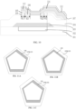
- FIG. 10 is a schematic sectional view of a bulk acoustic wave resonator according to an exemplary embodiment of the present disclosure, which is similarly taken along line 1A-1A in FIG. 1
- FIGS. 11A-11C are cross-sectional views for exemplarily illustrating an insertion layer in FIG. 10 , respectively.
- the widths of the frame edges of the insertion sub-frame formed by the protrusion structure 106 are different, that is, the width d21 of at least one frame edge is different from, for example, the width d22 of the remaining frame edges.
- the electromechanical coupling coefficient can be further adjusted or selected by changing the widths of the frame edges of the insertion sub-frame formed by the protrusion structure 106 and a proportion of the number of frame edges with each width to the number of five edges.
- the widths of the frame edges of the insertion sub-frame formed by the air gap 109 are different, that is, the width d11 of at least one frame edge is different from, for example, the width d12 of the remaining frame edges.
- the electromechanical coupling coefficient can be further adjusted or selected by changing the widths of the frame edges of the insertion sub-frame formed by the air gap 109 and s proportion of the number of frame edges with each width to the number of five edges.
- the widths of the frame edges of the insertion sub-frame formed by the protrusion structure 106 are different, and the widths of the frame edges of the insertion sub-frame formed by the air gap 109 are different.
- the electromechanical coupling coefficient can be further adjusted or selected by changing the widths of the frame edges of the insertion sub-frame formed by the protrusion structure 106, the widths of the frame edges of the insertion sub-frame formed by the air gap 109, and a proportion of the number of frame edges with each width to the number of five edges.
- the frame edges of the insertion frame in FIGS. 11A-11C are straight lines. Although not shown, the frame edges of the insertion frame in FIGS. 11A-11C may also have concave-convex shapes.
- the insertion layer is arranged between the piezoelectric layer and the top electrode, but the present disclosure is not limited thereto.
- the insertion layer may be arranged between the piezoelectric layer and the bottom electrode.
- the widths of the frame edges of the insertion frame of the insertion layer are different in the length direction of the frame edges, but a single frame edge of the insertion frame of the insertion layer may change in the length direction thereof.
- the thickness of the insertion layer is less than that of the top electrode.
- the electromechanical coupling coefficient of the resonator can be further adjusted by changing the width values of the insertion layer (e. g., corresponding to one or more of 105, 106, and 109) on different edges of the resonator, so that the design requirements can be satisfied and the design difficulty is reduced.
- the inventors have more choices during the development, and the limitation of the resonator frequency to the electromechanical coupling coefficient is removed.
- the electronic device herein includes, but is not limited to, intermediate products such as a radio-frequency front end and a filtering and amplifying module, and terminal products such as a mobile phone, WIFI and an unmanned aerial vehicle.
Landscapes
- Physics & Mathematics (AREA)
- Acoustics & Sound (AREA)
- Chemical & Material Sciences (AREA)
- Crystallography & Structural Chemistry (AREA)
- Piezo-Electric Or Mechanical Vibrators, Or Delay Or Filter Circuits (AREA)
Applications Claiming Priority (2)
| Application Number | Priority Date | Filing Date | Title |
|---|---|---|---|
| CN202010376103.3A CN111786645B (zh) | 2020-05-07 | 2020-05-07 | 体声波谐振器、滤波器、电子设备和调整机电耦合系数的方法 |
| PCT/CN2021/092059 WO2021223731A1 (zh) | 2020-05-07 | 2021-05-07 | 体声波谐振器、滤波器、电子设备和调整机电耦合系数的方法 |
Publications (2)
| Publication Number | Publication Date |
|---|---|
| EP4148997A1 true EP4148997A1 (de) | 2023-03-15 |
| EP4148997A4 EP4148997A4 (de) | 2024-04-03 |
Family
ID=72753119
Family Applications (1)
| Application Number | Title | Priority Date | Filing Date |
|---|---|---|---|
| EP21800399.4A Pending EP4148997A4 (de) | 2020-05-07 | 2021-05-07 | Volumenschallwellenresonator, filter, elektronische vorrichtung und verfahren zur einstellung eines elektromechanischen kopplungskoeffizienten |
Country Status (3)
| Country | Link |
|---|---|
| EP (1) | EP4148997A4 (de) |
| CN (1) | CN111786645B (de) |
| WO (1) | WO2021223731A1 (de) |
Cited By (3)
| Publication number | Priority date | Publication date | Assignee | Title |
|---|---|---|---|---|
| EP4333298A1 (de) * | 2022-08-30 | 2024-03-06 | Qorvo US, Inc. | Baw-resonator mit zweistufiger oxidrandringstruktur |
| US12081194B2 (en) | 2019-01-14 | 2024-09-03 | Qorvo Us, Inc. | Top electrodes and dielectric spacer layers for bulk acoustic wave resonators |
| WO2025211111A1 (ja) * | 2024-04-01 | 2025-10-09 | 株式会社村田製作所 | 弾性波フィルタ、マルチプレクサ、高周波フロントエンド回路及び通信装置 |
Families Citing this family (7)
| Publication number | Priority date | Publication date | Assignee | Title |
|---|---|---|---|---|
| CN111786645B (zh) * | 2020-05-07 | 2021-04-16 | 诺思(天津)微系统有限责任公司 | 体声波谐振器、滤波器、电子设备和调整机电耦合系数的方法 |
| US12483225B2 (en) | 2021-05-14 | 2025-11-25 | Skyworks Global Pte. Ltd. | Bulk acoustic wave resonator with oxide raised frame |
| KR20220163883A (ko) | 2021-06-03 | 2022-12-12 | 스카이워크스 글로벌 피티이. 엘티디. | 횡방향으로 분포된 반사기들을 갖는 라디오 주파수 음향 디바이스 |
| US20230006642A1 (en) * | 2021-07-02 | 2023-01-05 | Skyworks Global Pte. Ltd. | Radio frequency acoustic wave device with imbalanced raised frame |
| US12334908B2 (en) | 2021-12-10 | 2025-06-17 | Skyworks Solutions, Inc. | Bulk acoustic wave filters for improving noise factor |
| CN115622526A (zh) * | 2022-10-20 | 2023-01-17 | 北京芯溪半导体科技有限公司 | 一种体声波谐振器及其制备方法 |
| CN117081533B (zh) * | 2022-12-14 | 2024-06-04 | 北京芯溪半导体科技有限公司 | 一种体声波谐振器及其制备方法、滤波器和电子设备 |
Family Cites Families (24)
| Publication number | Priority date | Publication date | Assignee | Title |
|---|---|---|---|---|
| US5747705A (en) * | 1996-12-31 | 1998-05-05 | Honeywell Inc. | Method for making a thin film resonant microbeam absolute |
| FI108583B (fi) * | 1998-06-02 | 2002-02-15 | Nokia Corp | Resonaattorirakenteita |
| JP2006222562A (ja) * | 2005-02-08 | 2006-08-24 | Sony Corp | 微小共振器、バンドパスフィルタ、半導体装置、及び通信装置 |
| JP2006319796A (ja) * | 2005-05-13 | 2006-11-24 | Toshiba Corp | 薄膜バルク波音響共振器 |
| WO2007119556A1 (ja) * | 2006-04-05 | 2007-10-25 | Murata Manufacturing Co., Ltd. | 圧電共振子及び圧電フィルタ |
| US20120326807A1 (en) * | 2009-06-24 | 2012-12-27 | Avago Technologies Wireless Ip (Singapore) Pte. Ltd. | Acoustic resonator structure having an electrode with a cantilevered portion |
| US8384497B2 (en) * | 2009-12-18 | 2013-02-26 | Hao Zhang | Piezoelectric resonator structure having an interference structure |
| CN106209007B (zh) * | 2010-12-24 | 2019-07-05 | 株式会社村田制作所 | 弹性波装置 |
| US9991871B2 (en) * | 2011-02-28 | 2018-06-05 | Avago Technologies General Ip (Singapore) Pte. Ltd. | Bulk acoustic wave resonator comprising a ring |
| JP5994850B2 (ja) * | 2012-05-22 | 2016-09-21 | 株式会社村田製作所 | バルク波共振子 |
| KR101918031B1 (ko) * | 2013-01-22 | 2018-11-13 | 삼성전자주식회사 | 스퓨리어스 공진을 감소시키는 공진기 및 공진기 제작 방법 |
| EP3202034B1 (de) * | 2014-10-03 | 2020-05-06 | Teknologian Tutkimuskeskus VTT OY | Temperaturkompensierter zusammengesetzter resonator |
| US9571063B2 (en) * | 2014-10-28 | 2017-02-14 | Avago Technologies General Ip (Singapore) Pte. Ltd. | Acoustic resonator device with structures having different apodized shapes |
| JP5991566B1 (ja) * | 2015-01-28 | 2016-09-14 | 株式会社村田製作所 | 水晶振動子及びその製造方法並びに水晶振動デバイス |
| DE102015118437B4 (de) * | 2015-10-28 | 2017-11-16 | Snaptrack, Inc. | Schichtanordnung für ein Volumenwellenbauelement |
| DE102017118804B3 (de) * | 2017-08-17 | 2018-11-15 | RF360 Europe GmbH | Akustischer Resonator mit hohem Q |
| CN109889179A (zh) * | 2018-12-26 | 2019-06-14 | 天津大学 | 谐振器和梯形滤波器 |
| CN110061712B (zh) * | 2018-12-26 | 2023-10-20 | 天津大学 | 包括环形凸起梁檐结构的声学谐振器、滤波器和电子设备 |
| CN110120795B (zh) * | 2019-05-16 | 2022-11-22 | 西华大学 | 一种高品质因数的椭圆形谐振器 |
| CN111010128A (zh) * | 2019-06-05 | 2020-04-14 | 天津大学 | 带环形结构的谐振器、滤波器及电子设备 |
| CN111010119B (zh) * | 2019-08-15 | 2024-01-26 | 天津大学 | 带复合环形结构的谐振器、滤波器及电子设备 |
| CN111010120A (zh) * | 2019-09-20 | 2020-04-14 | 天津大学 | 具有调节层的体声波谐振器、滤波器和电子设备 |
| CN111010121A (zh) * | 2019-10-18 | 2020-04-14 | 天津大学 | 带不导电插入层的体声波谐振器、滤波器和电子设备 |
| CN111786645B (zh) * | 2020-05-07 | 2021-04-16 | 诺思(天津)微系统有限责任公司 | 体声波谐振器、滤波器、电子设备和调整机电耦合系数的方法 |
-
2020
- 2020-05-07 CN CN202010376103.3A patent/CN111786645B/zh active Active
-
2021
- 2021-05-07 EP EP21800399.4A patent/EP4148997A4/de active Pending
- 2021-05-07 WO PCT/CN2021/092059 patent/WO2021223731A1/zh not_active Ceased
Cited By (4)
| Publication number | Priority date | Publication date | Assignee | Title |
|---|---|---|---|---|
| US12081194B2 (en) | 2019-01-14 | 2024-09-03 | Qorvo Us, Inc. | Top electrodes and dielectric spacer layers for bulk acoustic wave resonators |
| US12425002B2 (en) | 2019-01-14 | 2025-09-23 | Qorvo Us, Inc. | Top electrodes and dielectric spacer layers for bulk acoustic wave resonators |
| EP4333298A1 (de) * | 2022-08-30 | 2024-03-06 | Qorvo US, Inc. | Baw-resonator mit zweistufiger oxidrandringstruktur |
| WO2025211111A1 (ja) * | 2024-04-01 | 2025-10-09 | 株式会社村田製作所 | 弾性波フィルタ、マルチプレクサ、高周波フロントエンド回路及び通信装置 |
Also Published As
| Publication number | Publication date |
|---|---|
| CN111786645A (zh) | 2020-10-16 |
| CN111786645B (zh) | 2021-04-16 |
| EP4148997A4 (de) | 2024-04-03 |
| WO2021223731A1 (zh) | 2021-11-11 |
Similar Documents
| Publication | Publication Date | Title |
|---|---|---|
| EP4148997A1 (de) | Volumenschallwellenresonator, filter, elektronische vorrichtung und verfahren zur einstellung eines elektromechanischen kopplungskoeffizienten | |
| EP4142152A1 (de) | Filter, volumenschallwellenresonatoranordnung und verfahren zur herstellung davon und elektronische vorrichtung | |
| EP4087132A1 (de) | Akustischer volumenresonator, filter, elektronische vorrichtung, verfahren zur einstellung des elektromechanischen kopplungskoeffizienten | |
| US6924717B2 (en) | Tapered electrode in an acoustic resonator | |
| US6812619B1 (en) | Resonator structure and a filter comprising such a resonator structure | |
| EP4033660A1 (de) | Volumenwellenresonator mit anpassungsschicht sowie filter und elektronische vorrichtung | |
| KR100489828B1 (ko) | Fbar 소자 및 그 제조방법 | |
| US7649304B2 (en) | Piezoelectric resonator and piezoelectric filter | |
| KR100698985B1 (ko) | 필터 및 필터의 제조 방법 | |
| US20130176085A1 (en) | Hybrid bulk acoustic wave resonator | |
| US20070080611A1 (en) | Aluminum nitride thin film, composite film containing the same and piezoelectric thin film resonator using the same | |
| EP1914888A1 (de) | Abzweigfilter | |
| US20040130847A1 (en) | Piezoelectric resonator device having detuning layer sequence | |
| JP2007036829A (ja) | 薄膜圧電共振器、フィルタ及び薄膜圧電共振器の製造方法 | |
| EP4027519A1 (de) | Volumenwellenresonator und verfahren zu seiner herstellung, filter und elektronische vorrichtung | |
| US8471435B2 (en) | Boundary acoustic wave device and method of manufacturing same | |
| CN113328714A (zh) | 压电结构及其制造方法以及包括该压电结构的压电谐振器 | |
| KR102691309B1 (ko) | 체적 음향 공진기 | |
| DE102016109829B4 (de) | Akustischer Resonator-Aufbau mit einer Mehrzahl von Kontakten an Verbindungsseiten | |
| WO2025236326A1 (zh) | 谐振器及其制备方法 | |
| CN112953447A (zh) | 谐振器及电子设备 | |
| CN217037147U (zh) | 声学谐振器、包括其的滤波器和包括其的双工器和多工器 | |
| CN116418311A (zh) | 体声波谐振器 | |
| CN116208114A (zh) | 一种体声波谐振器及其制备方法 | |
| CN115149920B (zh) | 谐振器及其形成方法、电子设备 |
Legal Events
| Date | Code | Title | Description |
|---|---|---|---|
| STAA | Information on the status of an ep patent application or granted ep patent |
Free format text: STATUS: THE INTERNATIONAL PUBLICATION HAS BEEN MADE |
|
| PUAI | Public reference made under article 153(3) epc to a published international application that has entered the european phase |
Free format text: ORIGINAL CODE: 0009012 |
|
| STAA | Information on the status of an ep patent application or granted ep patent |
Free format text: STATUS: REQUEST FOR EXAMINATION WAS MADE |
|
| 17P | Request for examination filed |
Effective date: 20221206 |
|
| AK | Designated contracting states |
Kind code of ref document: A1 Designated state(s): AL AT BE BG CH CY CZ DE DK EE ES FI FR GB GR HR HU IE IS IT LI LT LU LV MC MK MT NL NO PL PT RO RS SE SI SK SM TR |
|
| DAV | Request for validation of the european patent (deleted) | ||
| DAX | Request for extension of the european patent (deleted) | ||
| RIC1 | Information provided on ipc code assigned before grant |
Ipc: H03H 9/60 20060101ALI20231005BHEP Ipc: H03H 9/58 20060101ALI20231005BHEP Ipc: H03H 9/13 20060101ALI20231005BHEP Ipc: H03H 9/17 20060101ALI20231005BHEP Ipc: H03H 9/05 20060101ALI20231005BHEP Ipc: H03H 9/02 20060101AFI20231005BHEP |
|
| A4 | Supplementary search report drawn up and despatched |
Effective date: 20240301 |
|
| RIC1 | Information provided on ipc code assigned before grant |
Ipc: H03H 9/60 20060101ALI20240226BHEP Ipc: H03H 9/58 20060101ALI20240226BHEP Ipc: H03H 9/13 20060101ALI20240226BHEP Ipc: H03H 9/17 20060101ALI20240226BHEP Ipc: H03H 9/05 20060101ALI20240226BHEP Ipc: H03H 9/02 20060101AFI20240226BHEP |