EP4170730A1 - Elektronische vorrichtung mit transistoren - Google Patents
Elektronische vorrichtung mit transistoren Download PDFInfo
- Publication number
- EP4170730A1 EP4170730A1 EP22201739.4A EP22201739A EP4170730A1 EP 4170730 A1 EP4170730 A1 EP 4170730A1 EP 22201739 A EP22201739 A EP 22201739A EP 4170730 A1 EP4170730 A1 EP 4170730A1
- Authority
- EP
- European Patent Office
- Prior art keywords
- semiconductor
- region
- doped
- transistors
- contact
- Prior art date
- Legal status (The legal status is an assumption and is not a legal conclusion. Google has not performed a legal analysis and makes no representation as to the accuracy of the status listed.)
- Pending
Links
Images







Classifications
-
- H—ELECTRICITY
- H10—SEMICONDUCTOR DEVICES; ELECTRIC SOLID-STATE DEVICES NOT OTHERWISE PROVIDED FOR
- H10D—INORGANIC ELECTRIC SEMICONDUCTOR DEVICES
- H10D30/00—Field-effect transistors [FET]
- H10D30/01—Manufacture or treatment
- H10D30/021—Manufacture or treatment of FETs having insulated gates [IGFET]
- H10D30/028—Manufacture or treatment of FETs having insulated gates [IGFET] of double-diffused metal oxide semiconductor [DMOS] FETs
- H10D30/0291—Manufacture or treatment of FETs having insulated gates [IGFET] of double-diffused metal oxide semiconductor [DMOS] FETs of vertical DMOS [VDMOS] FETs
- H10D30/0297—Manufacture or treatment of FETs having insulated gates [IGFET] of double-diffused metal oxide semiconductor [DMOS] FETs of vertical DMOS [VDMOS] FETs using recessing of the gate electrodes, e.g. to form trench gate electrodes
-
- H—ELECTRICITY
- H10—SEMICONDUCTOR DEVICES; ELECTRIC SOLID-STATE DEVICES NOT OTHERWISE PROVIDED FOR
- H10D—INORGANIC ELECTRIC SEMICONDUCTOR DEVICES
- H10D30/00—Field-effect transistors [FET]
- H10D30/60—Insulated-gate field-effect transistors [IGFET]
- H10D30/64—Double-diffused metal-oxide semiconductor [DMOS] FETs
- H10D30/66—Vertical DMOS [VDMOS] FETs
- H10D30/668—Vertical DMOS [VDMOS] FETs having trench gate electrodes, e.g. UMOS transistors
-
- H—ELECTRICITY
- H10—SEMICONDUCTOR DEVICES; ELECTRIC SOLID-STATE DEVICES NOT OTHERWISE PROVIDED FOR
- H10D—INORGANIC ELECTRIC SEMICONDUCTOR DEVICES
- H10D62/00—Semiconductor bodies, or regions thereof, of devices having potential barriers
- H10D62/10—Shapes, relative sizes or dispositions of the regions of the semiconductor bodies; Shapes of the semiconductor bodies
- H10D62/124—Shapes, relative sizes or dispositions of the regions of semiconductor bodies or of junctions between the regions
- H10D62/126—Top-view geometrical layouts of the regions or the junctions
- H10D62/127—Top-view geometrical layouts of the regions or the junctions of cellular field-effect devices, e.g. multicellular DMOS transistors or IGBTs
-
- H—ELECTRICITY
- H10—SEMICONDUCTOR DEVICES; ELECTRIC SOLID-STATE DEVICES NOT OTHERWISE PROVIDED FOR
- H10D—INORGANIC ELECTRIC SEMICONDUCTOR DEVICES
- H10D62/00—Semiconductor bodies, or regions thereof, of devices having potential barriers
- H10D62/10—Shapes, relative sizes or dispositions of the regions of the semiconductor bodies; Shapes of the semiconductor bodies
- H10D62/13—Semiconductor regions connected to electrodes carrying current to be rectified, amplified or switched, e.g. source or drain regions
- H10D62/149—Source or drain regions of field-effect devices
- H10D62/151—Source or drain regions of field-effect devices of IGFETs
- H10D62/152—Source regions of DMOS transistors
- H10D62/153—Impurity concentrations or distributions
-
- H—ELECTRICITY
- H10—SEMICONDUCTOR DEVICES; ELECTRIC SOLID-STATE DEVICES NOT OTHERWISE PROVIDED FOR
- H10D—INORGANIC ELECTRIC SEMICONDUCTOR DEVICES
- H10D62/00—Semiconductor bodies, or regions thereof, of devices having potential barriers
- H10D62/10—Shapes, relative sizes or dispositions of the regions of the semiconductor bodies; Shapes of the semiconductor bodies
- H10D62/17—Semiconductor regions connected to electrodes not carrying current to be rectified, amplified or switched, e.g. channel regions
- H10D62/393—Body regions of DMOS transistors or IGBTs
-
- H—ELECTRICITY
- H10—SEMICONDUCTOR DEVICES; ELECTRIC SOLID-STATE DEVICES NOT OTHERWISE PROVIDED FOR
- H10D—INORGANIC ELECTRIC SEMICONDUCTOR DEVICES
- H10D64/00—Electrodes of devices having potential barriers
- H10D64/01—Manufacture or treatment
-
- H—ELECTRICITY
- H10—SEMICONDUCTOR DEVICES; ELECTRIC SOLID-STATE DEVICES NOT OTHERWISE PROVIDED FOR
- H10D—INORGANIC ELECTRIC SEMICONDUCTOR DEVICES
- H10D64/00—Electrodes of devices having potential barriers
- H10D64/111—Field plates
- H10D64/117—Recessed field plates, e.g. trench field plates or buried field plates
-
- H—ELECTRICITY
- H10—SEMICONDUCTOR DEVICES; ELECTRIC SOLID-STATE DEVICES NOT OTHERWISE PROVIDED FOR
- H10P—GENERIC PROCESSES OR APPARATUS FOR THE MANUFACTURE OR TREATMENT OF DEVICES COVERED BY CLASS H10
- H10P30/00—Ion implantation into wafers, substrates or parts of devices
- H10P30/20—Ion implantation into wafers, substrates or parts of devices into semiconductor materials, e.g. for doping
- H10P30/202—Ion implantation into wafers, substrates or parts of devices into semiconductor materials, e.g. for doping characterised by the semiconductor materials
- H10P30/204—Ion implantation into wafers, substrates or parts of devices into semiconductor materials, e.g. for doping characterised by the semiconductor materials into Group IV semiconductors
-
- H—ELECTRICITY
- H10—SEMICONDUCTOR DEVICES; ELECTRIC SOLID-STATE DEVICES NOT OTHERWISE PROVIDED FOR
- H10P—GENERIC PROCESSES OR APPARATUS FOR THE MANUFACTURE OR TREATMENT OF DEVICES COVERED BY CLASS H10
- H10P30/00—Ion implantation into wafers, substrates or parts of devices
- H10P30/20—Ion implantation into wafers, substrates or parts of devices into semiconductor materials, e.g. for doping
- H10P30/21—Ion implantation into wafers, substrates or parts of devices into semiconductor materials, e.g. for doping of electrically active species
-
- H—ELECTRICITY
- H10—SEMICONDUCTOR DEVICES; ELECTRIC SOLID-STATE DEVICES NOT OTHERWISE PROVIDED FOR
- H10P—GENERIC PROCESSES OR APPARATUS FOR THE MANUFACTURE OR TREATMENT OF DEVICES COVERED BY CLASS H10
- H10P30/00—Ion implantation into wafers, substrates or parts of devices
- H10P30/20—Ion implantation into wafers, substrates or parts of devices into semiconductor materials, e.g. for doping
- H10P30/28—Ion implantation into wafers, substrates or parts of devices into semiconductor materials, e.g. for doping characterised by an annealing step, e.g. for activation of dopants
-
- H—ELECTRICITY
- H10—SEMICONDUCTOR DEVICES; ELECTRIC SOLID-STATE DEVICES NOT OTHERWISE PROVIDED FOR
- H10D—INORGANIC ELECTRIC SEMICONDUCTOR DEVICES
- H10D62/00—Semiconductor bodies, or regions thereof, of devices having potential barriers
- H10D62/10—Shapes, relative sizes or dispositions of the regions of the semiconductor bodies; Shapes of the semiconductor bodies
- H10D62/13—Semiconductor regions connected to electrodes carrying current to be rectified, amplified or switched, e.g. source or drain regions
- H10D62/149—Source or drain regions of field-effect devices
- H10D62/151—Source or drain regions of field-effect devices of IGFETs
- H10D62/152—Source regions of DMOS transistors
- H10D62/154—Dispositions
-
- H—ELECTRICITY
- H10—SEMICONDUCTOR DEVICES; ELECTRIC SOLID-STATE DEVICES NOT OTHERWISE PROVIDED FOR
- H10D—INORGANIC ELECTRIC SEMICONDUCTOR DEVICES
- H10D62/00—Semiconductor bodies, or regions thereof, of devices having potential barriers
- H10D62/10—Shapes, relative sizes or dispositions of the regions of the semiconductor bodies; Shapes of the semiconductor bodies
- H10D62/13—Semiconductor regions connected to electrodes carrying current to be rectified, amplified or switched, e.g. source or drain regions
- H10D62/149—Source or drain regions of field-effect devices
- H10D62/151—Source or drain regions of field-effect devices of IGFETs
- H10D62/152—Source regions of DMOS transistors
- H10D62/155—Shapes
Definitions
- the present description generally relates to electronic devices, and more particularly to electronic devices comprising transistors.
- field-effect transistors are used in a non-conducting state to block high voltages, typically greater than 10 V, for example of the order of 40 V, or even greater than 100 V.
- Such transistors with field effect are generally adapted to block a high drain-source voltage only when the drain-source voltage is positive.
- An object of an embodiment is to provide an electronic device comprising transistors overcoming all or part of the drawbacks of existing transistor electronic devices.
- the surface occupied by the field effect transistors is reduced.
- the manufacturing cost of the field effect transistors is reduced.
- One embodiment provides an electronic device comprising a semiconductor substrate having a first face and transistors whose gates are contained in trenches extending in the substrate semiconductor, each transistor comprising, in the semiconductor substrate, a semiconductor box doped with a first type of conductivity, in which the channel of the transistor is formed in operation, the box being buried in the semiconductor substrate and in contact with two adjacent trenches among said trenches, a first semiconductor region doped with a second type of conductivity, opposite the first type of conductivity, covering the well, in contact with the well, and in contact with the two adjacent trenches, a second semiconductor region doped with the second type of conductivity more heavily doped than the first semiconductor region, extending into the first semiconductor region and exposed on the first side, and a third doped semiconductor region of the first conductivity type, more heavily doped than the well, covering the well, exposed on the first face, in contact with the first region, and extending into the semiconductor substrate in contact with the well.
- the second semiconductor region is in contact with the two adjacent trenches.
- the third semiconductor region is in contact with the two adjacent trenches.
- the first semiconductor region comprises a first semiconductor sub-region containing the second semiconductor region and at least one second semiconductor sub-region exposed on the first face and connecting the first semiconductor sub-region to the third semiconductor region, the maximum depth of the first semiconductor sub-region being greater than the maximum depth of the second semiconductor sub-region.
- the second semiconductor regions of the transistors are electrically connected together and the third semiconductor regions of the transistors are electrically connected together.
- the semiconductor substrate comprises a second face opposite the first face, each transistor further comprising, in the semiconductor substrate, a fourth semiconductor region doped with the second type of conductivity, covered by the well, in contact with the well , and a fifth semiconductor region doped with the second type of conductivity, more heavily doped than the fourth semiconductor region, and exposed on the second face.
- the electronic device comprises several transistors for each pair of adjacent trenches, at least some of the third semiconductor regions of the transistors being alternated with the second semiconductor regions of the transistors.
- the wells of two adjacent transistors are contiguous.
- An embodiment also provides a method of manufacturing the electronic device as defined previously, in which the formation of the first semiconductor region comprises a step of forming, by epitaxy, a doped semiconductor layer of the second type of conductivity, and a step of implanting dopants of the second type of conductivity in the semiconductor layer.
- FIG. 1A, 1B , 1C, and 1D represent, partially and schematically, sectional views and a top view respectively, and the figure 2 is a perspective view of one embodiment of a device 100 comprising several transistors T.
- Sectional views 1B and 1C have parallel planes 1B-1B and 1C-1C as their respective sectional planes.
- the transistors T are partially represented on the figures 1A to 1D And 2 .
- the device 100 is typically an integrated circuit electronic chip, defined by a semiconductor substrate 102 comprising a front face 104 and a rear face 106, not visible on the figures 1A to 1D And 2 and visible on the figures 3A and 3B described later, opposite the front face 104, and transistors T located in and on the substrate 102.
- the transistors T are delimited by trenches 110, four parallel trenches 110 being represented by way of example on the figures 1B to 1D And 2 .
- Each trench 110 extends into the substrate 102 from the front face 104 over part of the thickness of the substrate 102.
- Each transistor T defined by the elements described above thus constitutes a field-effect transistor, that is to say an electronic component capable, depending on a control voltage applied between the gate 120 and the source region 150, to form, in the well 130, a conductive channel electrically connecting the drain and source regions 140 and 150.
- the gate 120 of each transistor T comprises at least one electrically conductive region extending in one of the trenches 110, such as for example a metal and/or doped polycrystalline silicon, a side wall of the trench 110 constituting a side face well 130 of transistor T.
- Gate insulator 124 covering the side wall of trench 110, is in contact with well 130 and with the conductive region of gate 120.
- Gate insulator 124 is typically made of one or more dielectric layers, for example the gate insulator consists of a layer of silicon oxide.
- the thickness of gate insulator 124 is typically less than 15 nm, preferably between 20 nm and 40 nm.
- each trench 110 can have a width of between 0.1 ⁇ m and 1 ⁇ m, for example equal to 0.6 ⁇ m.
- the trenches 110 extend at least in part along directions parallel to the same direction, referred to as the longitudinal trench direction hereafter, and are regularly spaced.
- the direction perpendicular to the longitudinal direction of the trench is called the trench lateral direction.
- the pitch of the trenches in the lateral trench direction can be between 0.9 ⁇ m and 1.2 ⁇ m.
- the number of trenches 110 can vary from 1000 to 3000.
- the length of each trench 110 according to the longitudinal direction of the trench can vary from 0.5 ⁇ m to 3 ⁇ m.
- each trench 110 of a set of adjacent and parallel trenches 110 delimits transistors T on either side of the trench 110
- the gates 120 contained in the trench 110 are connected to each other and form a gate 120 common to the transistors T which are delimited by this trench 110.
- the wells semiconductors 130 of the transistors T which are delimited by this trench 110 and located on the same side of this trench 110 are contiguous and form a continuous semiconductor box 130.
- the substrate 102 consists of a semiconductor wafer, for example a silicon wafer.
- the substrate consists of a layer located on the surface of a semiconductor wafer, for example an epitaxial layer on a semiconductor wafer.
- substrate 102 is monocrystalline.
- each box 130 located between first and second adjacent trenches 110 extends from the first trench 110, in contact with the gate insulator 124 covering the side wall of the first trench 110, up to the second trench, in contact of the gate insulator 124 covering the side wall of the second trench 110.
- the depth, measured from the front face 104, of the contact making zone 132 can be between 0.4 ⁇ m and 0.8 ⁇ m.
- the maximum depth, measured from the front face 104, of the box 130 can be between 0.8 ⁇ m and 1.2 ⁇ m.
- the thickness, measured in a direction orthogonal to the front face 104, of the box 130 under the drift region 152 can be between 0.5 ⁇ m and 0.8 ⁇ m.
- the maximum thickness, measured in a direction orthogonal to the front face 104, of the box 130 can be between 1 ⁇ m and 1.3 ⁇ m.
- the dimension along the longitudinal trench direction of the contact zone 132 can be between 0.5 ⁇ m and 1.5 ⁇ m.
- each drift region 152 located between first and second adjacent trenches 110 extends from the first trench 110, in contact with the gate insulator 124 covering the side wall of the first trench 110, up to the second trench, in contact with the gate insulator 124 covering the side wall of the second trench 110.
- the drift region 152 comprises a first drift sub-region 154 and two second drift sub-regions 156, connected to the first sub-region first drift subregion 154 is less heavily doped than source region 150.
- Second drift subregions 156 are less heavily doped than source region 150, and preferably less heavily doped than source region 150.
- Each of the first drift sub-region 154 and second drift sub-regions 156 located between first and second adjacent trenches 110 extends from the first trench 110, in contact with the gate insulator 124 covering the side wall of the first trench 110, up to the second trench, in contact with the gate insulator 124 covering the side wall of the second trench 110.
- the source region 150 is contained in the first drift sub-region 154.
- the first sub-region 154 covers the entire bottom of the source region 150.
- the first sub-drift region 154 covers all of the side walls of the source region 150 between the first and second trenches 110.
- the second sub-drift regions 156 are located on either side of the first drift sub-region 154 in the longitudinal direction of the trench.
- Each second drift sub-region 156 extends, in the longitudinal direction of the trench, from the first drift sub-region 154 to the contact zone 132 adjacent to it.
- Each second sub-drift region 156 may be exposed on the front face 104 of the substrate 102.
- the source region 150 extends from the first trench 110, in contact with the gate insulator 124 covering the side wall from the first trench 110, to the second trench, in contact with the gate insulator 124 covering the side wall of the second trench 110
- the depth of the first drift sub-region 154 can be between 0.4 ⁇ m and 0.6 ⁇ m.
- the depth of each second drift sub-region 156 can be between 0.3 ⁇ m and 0.6 ⁇ m.
- the maximum dimension along the longitudinal trench direction of the drift region 152 can be between 2 ⁇ m and 5 ⁇ m.
- the dimension along the longitudinal trench direction of the first drift sub-region 154 can be between 1.5 ⁇ m and 4 ⁇ m.
- the dimension along the longitudinal trench direction of each second drift sub-region 156 can be between 0.5 ⁇ m and 1 ⁇ m.
- the depth, measured from the first face 104, of the source region 150 can be between 0.2 ⁇ m and 0.4 ⁇ m.
- transistor T is of the N-channel type.
- doped zones 140 and 150 are N-type doped.
- Well 130 is P-type doped.
- the types N and P conductivity, or doping types can be interchanged. Functionings similar to those described are then obtained by exchanging the signs of the voltages in the device.
- the doping levels of zones 140 and 150 are high, that is to say greater than 5*10 18 atoms/cm 3 , preferably greater than 10 19 atoms/cm 3 .
- Contact point 132 electrically connected to well 130, is a doped zone also having such a high doping level.
- the doping level of well 130 is preferably less than 10 18 atoms/cm 3 , more preferably less than 5*10 17 atoms/cm 3 .
- Each drift region 142, 152 has a doping level lower than that of the doped zone 150.
- each semiconductor region 142, 152 has a low doping level, that is to say less than 2*10 17 atoms/cm 3 .
- each first drift subregion 154 has a doping level of between 2*10 17 atoms/cm 3 and 6*10 17 atoms/cm 3 .
- each second drift sub-region 156 has a doping level of between 3*10 16 atoms/cm 3 and 1*10 17 atoms/cm 3 .
- the device 100 may further comprise, for each trench 110, an electrically conductive element 180 located in the trench 110.
- the conductive element 180 is connected to a terminal not shown on the figures 1A to 1D And 2 . This terminal is preferably connected to the zones of contact points 132.
- the conductive element 180 is located opposite at least a part of the semiconductor region 142, that is to say that the conductive element 180 is located against an insulator 184 covering the side face of at least a portion of the semiconductor region 142.
- the insulating layer 184 separates the conductive element 180 from the semiconductor region 142.
- the distance between the conductive element 180 and the semiconductor region 142, corresponding to the thickness of the insulating layer 184, is for example between 100 nm and 200 nm, preferably between 120 nm and 180 nm.
- Insulating layer 184 preferably has a thickness greater than that of gate insulator 124.
- insulating layer 184 is made of silicon oxide or silicon nitride.
- an insulating portion preferably a portion of the insulating layer 184, is located under the conductive element 180. This portion electrically insulates the conductive element 180 from the part of the substrate 102 located under the element conductor 180. Additionally, insulating layers 186, preferably of the same material or materials as gate insulator 124, electrically insulate conductive member 180 from gate 120.
- the conductive element 180 is constituted by a conductive wall located in a central part of the trench 110.
- the wall is elongated in the same direction as the trench.
- the wall extends into the substrate 102 orthogonal to the front face 104 of the substrate.
- the wall comprises, preferably consists of, a metallic material or, preferably, doped polysilicon.
- the width of the conductive wall, taken in the transverse trench direction, is for example between 30 nm and 200 nm.
- the device 100 further comprises conductive tracks and conductive vias, not shown on the figures 1A to 1D And 2 , at least one level of metallization formed on the front face 104 of the substrate 102 for the connections of the sources, the gates, and the wells of the transistors T.
- the source regions 150 of the set of MOS transistors are connected together.
- the gates 120 present in the trenches 110 are connected together.
- the contact zones 132 of the boxes 30 are connected together.
- FIGS. 3A and 3B are views analogous respectively to figures 1A and 1B illustrating an embodiment of the connections of the transistors T.
- the device 100 is represented on the figures 3A and 3B with two levels of metallization N1 and N2.
- the first level of metallization N1 comprises an insulating layer 190 covering the front face 104 of the substrate 102, metal tracks 192 extending over the insulating layer 190, and conductive vias 194 passing through the insulating layer 190 and connecting the metal tracks 192 in particular to the gates 120, to the source regions 150, and to the contact zones 132.
- the second level of metallization N2 comprises an insulating layer 200 covering the conductive tracks 192 and the insulating layer 190 between the conductive tracks 192, metal tracks 202 extending over the insulating layer 200, and conductive vias 204 passing through the insulating layer 200 and connecting the metal tracks 202 to at least some of the metal tracks 192.
- the device 100 comprises from 3*10 5 to 3*10 6 transistors T.
- FIG 4 is a top view of an embodiment illustrating an arrangement of conductive tracks 192 of the first metallization level which have the form of parallel strips and plates.
- the conductive vias 194 are further represented by squares possibly crossed by a horizontal line.
- the trenches 110 are parallel and extend without interruption over the entire region where the transistors are formed.
- the conductive tracks 192 are divided into conductive plates 192_S connected to the source regions 150 by conductive vias 194_S, into conductive tracks 192_B connected to the contact making zones 132 by vias 194_B, into a conductive track 192_G connected to the gates 120 by vias 194_G, and in a conductive track 192_M connected to the conductive elements 180 by vias 194_M.
- plates 192_S are alternated with strips 192_B.
- the conductive tracks 202 of the second metallization level can be used for the connection of 192_S conductor plates.
- FIG 5 is a top view of an embodiment illustrating another arrangement of the conductive tracks 192 of the first level of metallization which have the form of parallel strips and plates. We have also represented in figure 5 the boundaries of trenches 110, contact areas 132, and source regions 150.
- trenches 110 are parallel and extend and are distributed into sets 112 of trenches 110 over the region where the transistors are formed, each set 112 of trenches comprises first and second groups 114, 116 of trenches 110, the trenches of the first group 114 being offset in the transverse direction of the trench relative to the trenches 110 of the second group 116 by half the pitch of the trenches, the trenches of the first and second groups being connected at one end to a trench 118 extending in the direction trench cross section.
- the conductive vias 194 are represented by squares possibly crossed by a horizontal line.
- the conductive tracks 192 are divided into conductive plates 192_S connected to the source regions 150 by conductive vias 194_S, into conductive tracks 192_MB connected to the contact making zones 132 and to the conductive elements 180 by vias 194_MB.
- the connection of the grids 120 can be made in an area outside the figure 5 .
- the drain of the transistors T can be brought in operation to a potential of 40 V to 45 V.
- the voltage between the gate and the source of each transistor T is about 10 V and the potential at the source is about 40 V-45 V.
- the voltage between the gate and source of each transistor T is approximately 0 V and the source potential is approximately 0 V. 0V.
- conductive elements 180 advantageously makes it possible to reduce the intensity of the electric field present in operation at the level of the PN junctions. This makes it possible to increase the concentration of dopants of the drift region 142 and 152 while ensuring that the transistor is not damaged during the application of maximum voltages.
- THE figures 6 to 14 are sectional, partial and schematic views of structures obtained at stages of an embodiment of a method of manufacturing the device 100 of the figures 1A to 1D .
- FIG 12 , 13 , And 14 there are shown three sectional views A, B, and C similar to sectional views 1A, 1B, and 1C.
- FIG 6 represents the structure obtained after the formation in the substrate 102 of the heavily doped drain region 140 of the second type of conductivity, for example N-type doped, and of a semiconductor layer 210 more lightly doped than the drain region 140, of which the dopant concentration substantially corresponds to the desired dopant concentration for the drift region 142.
- the substrate 102 can be fabricated by forming, on a highly doped silicon wafer, which corresponds to the drain region 140, the silicon semiconductor 210 more weakly doped, for example by epitaxy.
- FIG. 7 represents the structure obtained after the formation of the trenches 110 in the layer 310 of the substrate 102.
- the trenches 110 can be produced by an etching step.
- FIG 8 represents the structure obtained after the formation, on the walls and the bottom of each trench 110, of an insulating layer 212.
- the method can comprise a conformal deposition of an insulating layer covering the structure resulting from the etching of the trenches 110.
- the composition and thickness of insulating layer 212 correspond to the composition and thickness desired for insulating layer 184.
- insulating layer 212 may be formed by a thermal oxidation step.
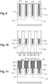
- FIG 9 represents the structure obtained after the formation in each trench 110 of a conductive core 214.
- the method may comprise the deposition of a conductive layer, for example in polycrystalline silicon, covering the insulating layer 212 and filling the remaining space of each trench 110, and the removal, for example by etching, of the parts of the conductive layer located outside the trenches 110.
- the composition of the conductive cores 214 corresponds to the desired composition of the conductive elements 180.
- FIG 10 represents the structure obtained after the etching, over part of the depth of each trench 110, of the insulating layer 212 and of the conductive core 214.
- the conductive elements 180 and the insulating layers 184 of the transistors are thus formed.
- FIG 11 represents the structure obtained after the formation, in each trench 110, of the insulating layer 186, of the gate insulator 124 and of the gate 120.
- the gate insulator 124 can be formed by thermal oxidation.
- the method may include depositing a conductive layer covering the insulating layer and filling the remaining space of each trench 110, and removing, for example by etching, the parts of the conductive layer located outside the trenches 110.
- FIG. 12 represents, in sectional views 12A, 12B, and 12C, the structure obtained after a step of implanting dopants of the first type of conductivity, for example of type P, to form the wells 130 of the transistors, buried in the substrate 102 .
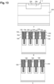
- FIG. 13 represents, in sectional views 13A, 13B, and 13C, the structure obtained after a first step of implanting dopants of the second type of conductivity, to form, for each transistor T, the first drift sub-region 154, and a second step of implanting dopants of the second type of conductivity, to form, for each transistor T, the source region 150.
- FIG. 14 represents, in cross-sectional views 14A, 14B, and 14C, the structure obtained after a step of implanting dopants of a first conductivity type to form the contact making zones 132. This further delimits, for each transistor T, the second drift sub-regions 156 of the drift regions 152. The transistors T are thus formed.
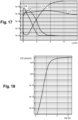
- THE figures 15 and 16 are perspective views with section along two different directions illustrating the evolution of the concentration of dopants in gray levels in the device 100 of the figures 1A to 1D manufactured according to the embodiment of the manufacturing method described above in relation to the figures 6 to 14 with the dopant concentration profiles illustrated on the figure 17 .
- the shade of gray is all the darker as the concentration of N- or P-type dopants is high.
- the semiconductor substrate 102 is shown and the elements of a single transistor T are partially shown.
- the contours of the gate 120, of the conductive element 180, and of the vias 194 connected to the source region 150 and the contact area 132 of the transistor T are also partially represented.
- the curves C1, C2, C3, and C4 are dopant concentration profiles, expressed in atoms/cm 3 , in the substrate 102 as a function of the depth measured from the front face 104 at the level of a source region 150
- the substrate 102 can be fabricated by forming, on a silicon wafer heavily doped with arsenic (N-type dopant), which corresponds to the drain region 140, and the semiconductor layer 210 of silicon more weakly doped with phosphorus (N-type dopant), for example by epitaxy.
- the curve C1 is the curve of evolution of the concentration of arsenic (present in the substrate 102) and the curve C2 is the curve of evolution of the concentration of phosphorus resulting from the formation of the layer 210.
- the curve C3 is the curve of evolution of the concentration of boron (type P dopant) obtained after the step of implantation for the formation of the box 130.
- the curve C4 is the curve of evolution of the concentration of phosphorus obtained after the step implantation for the formation of the first drift sub-region 154.
- the evolution curve, not represented in figure 5 of the phosphorus concentration obtained after the phosphorus implantation step for the formation of the source region 150 shows a peak at approximately 2*10 19 atoms/cm 3 at a depth of approximately 50 nm and drops to less than of 1*10 15 atoms/cm 3 at a depth greater than 350 nm.
- the concentration of N-type dopants changes continuously between the first and second drift sub-regions 154, 156 and the source region 150.
- Simulations have been carried out for the device 100 represented on the figures 1A to 1D to highlight the properties of the transistors T.
- the device 100 included the concentrations of dopants described previously in relation to the figures 15 to 17 .
- the simulations correspond to normal operating situations of transistor T and unfavorable potential conditions for the PN junctions of transistor T.
- the simulations were carried out for a temperature of 25°C.
- FIG 18 represents a curve of evolution of the current density CD, expressed in A/cm 2 , as a function of the drain voltage Vd, expressed in volts, circulating in the drain region 140 of transistor T in the on state.
- the figure 19 , 21 , And 23 are side sectional views of part of a transistor T and the figure 20 , 22 , And 24 are perspective views with section of part of a transistor T.
- the figures 19, 20 , 22 , And 24 illustrate the evolution of the current density in gray levels in different configurations of use of the transistor T.
- the current density CD is expressed in A/cm 2 and the shade of gray is all the darker as the current density takes on extreme high or extreme low values.
- the current density CD is expressed in A/cm 2 .
- THE figure 21 And 23 represent equipotentials in different configurations of use of the transistor T.
- the concentration of dopants is also represented in gray levels, the shade of gray is all the darker as the concentration of N- or P-type dopants is high.
- THE figures 18 to 20 illustrate a first simulation in which the transistor T is in the on state.
- the drain of transistor T was at a potential of about 40 V
- the voltage between the gate and the source of transistor T was about 10 V
- the potential at the source of transistor T was about 40 V.
- on-state resistance Ron substantially equal to 6.3 mohms.mm 2 was determined. The presence of contact zones 132 does not lead to excessive degradation of the on-state resistance Ron compared to a structure in which the source region would extend all along the trench.
- THE figures 21 and 22 illustrate a second simulation in which the transistor T is in the off state and the bias conditions of the PN junction between the well 130 and the drift region 142 are the most unfavorable.
- the drain of transistor T is at a potential about 40 V
- the voltage between the gate and the source of the transistor T was about 0 V
- the potential at the source of the transistor T was about 0 V.
- the PN junction formed between the well 130 and the drift region 142 is reverse biased and holds the applied potentials.
- THE figures 23 and 24 illustrate a third simulation in which the transistors T are in the off state and the bias conditions of the junction between the well 130 and the drift region 152 are the most unfavorable.
- the drain of each transistor T was at a potential of about 0 V
- the voltage between the gate and the source of each transistor T was about 0 V
- the potential at the source of each transistor T was about 17 V.
- the PN junction formed between well 130 and drift region 152 is reverse biased and holds the applied potentials.
- the transistors T described above advantageously allow voltage withstand in the off state both for a positive drain-source voltage and a negative drain-source voltage.
- transistors T have been described with a drain region 140 located on the rear face side.
- the drift region 142 can be in contact with a more doped contacting zone located on the side of the front face.
Landscapes
- Insulated Gate Type Field-Effect Transistor (AREA)
- Metal-Oxide And Bipolar Metal-Oxide Semiconductor Integrated Circuits (AREA)
- Engineering & Computer Science (AREA)
- Manufacturing & Machinery (AREA)
Applications Claiming Priority (1)
| Application Number | Priority Date | Filing Date | Title |
|---|---|---|---|
| FR2111151A FR3128312B1 (fr) | 2021-10-20 | 2021-10-20 | Dispositif électronique comprenant des transistors |
Publications (1)
| Publication Number | Publication Date |
|---|---|
| EP4170730A1 true EP4170730A1 (de) | 2023-04-26 |
Family
ID=80595289
Family Applications (1)
| Application Number | Title | Priority Date | Filing Date |
|---|---|---|---|
| EP22201739.4A Pending EP4170730A1 (de) | 2021-10-20 | 2022-10-14 | Elektronische vorrichtung mit transistoren |
Country Status (4)
| Country | Link |
|---|---|
| US (1) | US12593482B2 (de) |
| EP (1) | EP4170730A1 (de) |
| CN (2) | CN115995489A (de) |
| FR (1) | FR3128312B1 (de) |
Families Citing this family (1)
| Publication number | Priority date | Publication date | Assignee | Title |
|---|---|---|---|---|
| FR3128312B1 (fr) * | 2021-10-20 | 2025-02-28 | St Microelectronics Srl | Dispositif électronique comprenant des transistors |
Citations (3)
| Publication number | Priority date | Publication date | Assignee | Title |
|---|---|---|---|---|
| US20150263146A1 (en) * | 2014-03-13 | 2015-09-17 | Kabushiki Kaisha Toshiba | Semiconductor device |
| US20190288103A1 (en) * | 2018-03-16 | 2019-09-19 | Kabushiki Kaisha Toshiba | Semiconductor device |
| US20190305079A1 (en) * | 2018-03-27 | 2019-10-03 | Ablic Inc. | Semiconductor device and method of manufacturing the same |
Family Cites Families (18)
| Publication number | Priority date | Publication date | Assignee | Title |
|---|---|---|---|---|
| JP4097417B2 (ja) | 2001-10-26 | 2008-06-11 | 株式会社ルネサステクノロジ | 半導体装置 |
| US7719054B2 (en) * | 2006-05-31 | 2010-05-18 | Advanced Analogic Technologies, Inc. | High-voltage lateral DMOS device |
| JP3927111B2 (ja) * | 2002-10-31 | 2007-06-06 | 株式会社東芝 | 電力用半導体装置 |
| US8039892B2 (en) | 2007-04-26 | 2011-10-18 | Infineon Technologies Ag | Semiconductor device and a method for manufacturing a semiconductor device |
| US8779510B2 (en) | 2010-06-01 | 2014-07-15 | Alpha And Omega Semiconductor Incorporated | Semiconductor power devices manufactured with self-aligned processes and more reliable electrical contacts |
| US9048282B2 (en) * | 2013-03-14 | 2015-06-02 | Alpha And Omega Semiconductor Incorporated | Dual-gate trench IGBT with buried floating P-type shield |
| US8564047B2 (en) | 2011-09-27 | 2013-10-22 | Force Mos Technology Co., Ltd. | Semiconductor power devices integrated with a trenched clamp diode |
| US9401355B2 (en) | 2011-12-16 | 2016-07-26 | Infineon Technologies Ag | Semiconductor device including a diode arranged in a trench |
| US8772865B2 (en) | 2012-09-26 | 2014-07-08 | Semiconductor Components Industries, Llc | MOS transistor structure |
| US9230851B2 (en) * | 2013-02-07 | 2016-01-05 | Texas Instruments Incorporated | Reduction of polysilicon residue in a trench for polysilicon trench filling processes |
| CN103887342B (zh) | 2014-04-10 | 2018-11-02 | 矽力杰半导体技术(杭州)有限公司 | 沟槽mosfet及其制作方法 |
| US9472662B2 (en) | 2015-02-23 | 2016-10-18 | Freescale Semiconductor, Inc. | Bidirectional power transistor with shallow body trench |
| JP6822088B2 (ja) | 2016-11-15 | 2021-01-27 | 富士電機株式会社 | 炭化珪素半導体装置および炭化珪素半導体装置の製造方法 |
| DE102017108048A1 (de) | 2017-04-13 | 2018-10-18 | Infineon Technologies Austria Ag | Halbleitervorrichtung mit einer grabenstruktur |
| JP7324603B2 (ja) * | 2019-03-29 | 2023-08-10 | ローム株式会社 | 半導体装置 |
| FR3106697A1 (fr) | 2020-01-23 | 2021-07-30 | Stmicroelectronics (Rousset) Sas | Structure de transistor |
| FR3128312B1 (fr) * | 2021-10-20 | 2025-02-28 | St Microelectronics Srl | Dispositif électronique comprenant des transistors |
| FR3128823B1 (fr) * | 2021-10-29 | 2024-09-20 | St Microelectronics Rousset | Dispositif électronique comprenant des transistors |
-
2021
- 2021-10-20 FR FR2111151A patent/FR3128312B1/fr active Active
-
2022
- 2022-10-04 US US17/960,064 patent/US12593482B2/en active Active
- 2022-10-14 EP EP22201739.4A patent/EP4170730A1/de active Pending
- 2022-10-19 CN CN202211280672.3A patent/CN115995489A/zh active Pending
- 2022-10-19 CN CN202222753179.0U patent/CN219497802U/zh active Active
Patent Citations (3)
| Publication number | Priority date | Publication date | Assignee | Title |
|---|---|---|---|---|
| US20150263146A1 (en) * | 2014-03-13 | 2015-09-17 | Kabushiki Kaisha Toshiba | Semiconductor device |
| US20190288103A1 (en) * | 2018-03-16 | 2019-09-19 | Kabushiki Kaisha Toshiba | Semiconductor device |
| US20190305079A1 (en) * | 2018-03-27 | 2019-10-03 | Ablic Inc. | Semiconductor device and method of manufacturing the same |
Also Published As
| Publication number | Publication date |
|---|---|
| FR3128312A1 (fr) | 2023-04-21 |
| US20230121961A1 (en) | 2023-04-20 |
| CN115995489A (zh) | 2023-04-21 |
| US12593482B2 (en) | 2026-03-31 |
| FR3128312B1 (fr) | 2025-02-28 |
| CN219497802U (zh) | 2023-08-08 |
Similar Documents
| Publication | Publication Date | Title |
|---|---|---|
| KR100257412B1 (ko) | 집적회로 장치 | |
| US4980306A (en) | Method of making a CMOS device with trench isolation device | |
| FR2593640A1 (fr) | Dispositif semi-conducteur monolithique integre comportant des transistors a jonction bipolaire, des transistors cmos et dmos, des diodes a faible fuite et procede pour sa fabrication | |
| EP3629380A1 (de) | Diodenstruktur | |
| EP4174946A1 (de) | Elektronische vorrichtung mit transistoren | |
| FR2692402A1 (fr) | Dispositif à semiconducteurs comportant des couches semiconductrices de différents types de conductivité et procédé de fabrication. | |
| EP0581625B1 (de) | Multifunktionale elektronische Vorrichtung, insbesondere Element mit dynamischem, negativem Widerstandsverhalten und Zugehöriges Herstellungsverfahren | |
| EP3855506A1 (de) | Transistorkonstruktion | |
| FR3042907A1 (fr) | Procede de fabrication d'un dispositif a transistors mos | |
| FR2739976A1 (fr) | Structure de terminaison, dispositif a semi-conducteur, et leurs procedes de fabrication | |
| EP3745468A1 (de) | Transistorkonstruktion | |
| EP4170730A1 (de) | Elektronische vorrichtung mit transistoren | |
| FR3121780A1 (fr) | Cellule mémoire programmable et effaçable | |
| FR3114686A1 (fr) | Transistor MOS à triple grille et procédé de fabrication d’un tel transistor | |
| FR3005787A1 (fr) | Montage cascode de transistors pour l'amplification de signaux hautes frequences | |
| FR3068507A1 (fr) | Realisation de regions semiconductrices dans une puce electronique | |
| FR3080948A1 (fr) | Circuit integre comprenant un element capacitif, et procede de fabrication | |
| FR3054373A1 (fr) | Dispositif de protection contre des surtensions | |
| FR3067516A1 (fr) | Realisation de regions semiconductrices dans une puce electronique | |
| FR3095891A1 (fr) | Circuit électronique | |
| FR3109838A1 (fr) | Transistors contraints et mémoire à changement de phase | |
| EP3758053A1 (de) | Verfahren zur herstellung einer abstimmdiode und eines bipolartransistors | |
| EP4287263A1 (de) | Lateraler bipolartransistor | |
| EP0146430B1 (de) | Feldeffekttransistor mit regelbarer Schwellenspannung und integrierte Schaltung mit solchem Transistor | |
| FR3083367A1 (fr) | Circuit electronique |
Legal Events
| Date | Code | Title | Description |
|---|---|---|---|
| PUAI | Public reference made under article 153(3) epc to a published international application that has entered the european phase |
Free format text: ORIGINAL CODE: 0009012 |
|
| STAA | Information on the status of an ep patent application or granted ep patent |
Free format text: STATUS: REQUEST FOR EXAMINATION WAS MADE |
|
| 17P | Request for examination filed |
Effective date: 20221014 |
|
| AK | Designated contracting states |
Kind code of ref document: A1 Designated state(s): AL AT BE BG CH CY CZ DE DK EE ES FI FR GB GR HR HU IE IS IT LI LT LU LV MC ME MK MT NL NO PL PT RO RS SE SI SK SM TR |