EP4177934B1 - Procédé de préparation de structure semi-conductrice, structure semi-conductrice et mémoire semi-conductrice - Google Patents
Procédé de préparation de structure semi-conductrice, structure semi-conductrice et mémoire semi-conductrice Download PDFInfo
- Publication number
- EP4177934B1 EP4177934B1 EP21948687.5A EP21948687A EP4177934B1 EP 4177934 B1 EP4177934 B1 EP 4177934B1 EP 21948687 A EP21948687 A EP 21948687A EP 4177934 B1 EP4177934 B1 EP 4177934B1
- Authority
- EP
- European Patent Office
- Prior art keywords
- dielectric layer
- layer
- etching
- peripheral area
- isolation wall
- Prior art date
- Legal status (The legal status is an assumption and is not a legal conclusion. Google has not performed a legal analysis and makes no representation as to the accuracy of the status listed.)
- Active
Links
Images


Classifications
-
- H—ELECTRICITY
- H10—SEMICONDUCTOR DEVICES; ELECTRIC SOLID-STATE DEVICES NOT OTHERWISE PROVIDED FOR
- H10B—ELECTRONIC MEMORY DEVICES
- H10B12/00—Dynamic random access memory [DRAM] devices
- H10B12/01—Manufacture or treatment
- H10B12/09—Manufacture or treatment with simultaneous manufacture of the peripheral circuit region and memory cells
-
- H—ELECTRICITY
- H10—SEMICONDUCTOR DEVICES; ELECTRIC SOLID-STATE DEVICES NOT OTHERWISE PROVIDED FOR
- H10B—ELECTRONIC MEMORY DEVICES
- H10B12/00—Dynamic random access memory [DRAM] devices
- H10B12/30—DRAM devices comprising one-transistor - one-capacitor [1T-1C] memory cells
- H10B12/31—DRAM devices comprising one-transistor - one-capacitor [1T-1C] memory cells having a storage electrode stacked over the transistor
-
- H—ELECTRICITY
- H10—SEMICONDUCTOR DEVICES; ELECTRIC SOLID-STATE DEVICES NOT OTHERWISE PROVIDED FOR
- H10B—ELECTRONIC MEMORY DEVICES
- H10B12/00—Dynamic random access memory [DRAM] devices
- H10B12/30—DRAM devices comprising one-transistor - one-capacitor [1T-1C] memory cells
- H10B12/34—DRAM devices comprising one-transistor - one-capacitor [1T-1C] memory cells the transistor being at least partially in a trench in the substrate
-
- H—ELECTRICITY
- H10—SEMICONDUCTOR DEVICES; ELECTRIC SOLID-STATE DEVICES NOT OTHERWISE PROVIDED FOR
- H10B—ELECTRONIC MEMORY DEVICES
- H10B12/00—Dynamic random access memory [DRAM] devices
- H10B12/50—Peripheral circuit region structures
-
- H—ELECTRICITY
- H10—SEMICONDUCTOR DEVICES; ELECTRIC SOLID-STATE DEVICES NOT OTHERWISE PROVIDED FOR
- H10D—INORGANIC ELECTRIC SEMICONDUCTOR DEVICES
- H10D84/00—Integrated devices formed in or on semiconductor substrates that comprise only semiconducting layers, e.g. on Si wafers or on GaAs-on-Si wafers
- H10D84/80—Integrated devices formed in or on semiconductor substrates that comprise only semiconducting layers, e.g. on Si wafers or on GaAs-on-Si wafers characterised by the integration of at least one component covered by groups H10D12/00 or H10D30/00, e.g. integration of IGFETs
- H10D84/82—Integrated devices formed in or on semiconductor substrates that comprise only semiconducting layers, e.g. on Si wafers or on GaAs-on-Si wafers characterised by the integration of at least one component covered by groups H10D12/00 or H10D30/00, e.g. integration of IGFETs of only field-effect components
- H10D84/83—Integrated devices formed in or on semiconductor substrates that comprise only semiconducting layers, e.g. on Si wafers or on GaAs-on-Si wafers characterised by the integration of at least one component covered by groups H10D12/00 or H10D30/00, e.g. integration of IGFETs of only field-effect components of only insulated-gate FETs [IGFET]
- H10D84/8314—Integrated devices formed in or on semiconductor substrates that comprise only semiconducting layers, e.g. on Si wafers or on GaAs-on-Si wafers characterised by the integration of at least one component covered by groups H10D12/00 or H10D30/00, e.g. integration of IGFETs of only field-effect components of only insulated-gate FETs [IGFET] the IGFETs characterised by having gate insulating layers with different properties
-
- H—ELECTRICITY
- H10—SEMICONDUCTOR DEVICES; ELECTRIC SOLID-STATE DEVICES NOT OTHERWISE PROVIDED FOR
- H10P—GENERIC PROCESSES OR APPARATUS FOR THE MANUFACTURE OR TREATMENT OF DEVICES COVERED BY CLASS H10
- H10P50/00—Etching of wafers, substrates or parts of devices
- H10P50/20—Dry etching; Plasma etching; Reactive-ion etching
- H10P50/28—Dry etching; Plasma etching; Reactive-ion etching of insulating materials
-
- H—ELECTRICITY
- H10—SEMICONDUCTOR DEVICES; ELECTRIC SOLID-STATE DEVICES NOT OTHERWISE PROVIDED FOR
- H10D—INORGANIC ELECTRIC SEMICONDUCTOR DEVICES
- H10D84/00—Integrated devices formed in or on semiconductor substrates that comprise only semiconducting layers, e.g. on Si wafers or on GaAs-on-Si wafers
- H10D84/01—Manufacture or treatment
- H10D84/0123—Integrating together multiple components covered by H10D12/00 or H10D30/00, e.g. integrating multiple IGBTs
- H10D84/0126—Integrating together multiple components covered by H10D12/00 or H10D30/00, e.g. integrating multiple IGBTs the components including insulated gates, e.g. IGFETs
- H10D84/0128—Manufacturing their channels
-
- H—ELECTRICITY
- H10—SEMICONDUCTOR DEVICES; ELECTRIC SOLID-STATE DEVICES NOT OTHERWISE PROVIDED FOR
- H10D—INORGANIC ELECTRIC SEMICONDUCTOR DEVICES
- H10D84/00—Integrated devices formed in or on semiconductor substrates that comprise only semiconducting layers, e.g. on Si wafers or on GaAs-on-Si wafers
- H10D84/01—Manufacture or treatment
- H10D84/0123—Integrating together multiple components covered by H10D12/00 or H10D30/00, e.g. integrating multiple IGBTs
- H10D84/0126—Integrating together multiple components covered by H10D12/00 or H10D30/00, e.g. integrating multiple IGBTs the components including insulated gates, e.g. IGFETs
- H10D84/0144—Manufacturing their gate insulating layers
-
- H—ELECTRICITY
- H10—SEMICONDUCTOR DEVICES; ELECTRIC SOLID-STATE DEVICES NOT OTHERWISE PROVIDED FOR
- H10D—INORGANIC ELECTRIC SEMICONDUCTOR DEVICES
- H10D84/00—Integrated devices formed in or on semiconductor substrates that comprise only semiconducting layers, e.g. on Si wafers or on GaAs-on-Si wafers
- H10D84/01—Manufacture or treatment
- H10D84/0123—Integrating together multiple components covered by H10D12/00 or H10D30/00, e.g. integrating multiple IGBTs
- H10D84/0126—Integrating together multiple components covered by H10D12/00 or H10D30/00, e.g. integrating multiple IGBTs the components including insulated gates, e.g. IGFETs
- H10D84/0165—Integrating together multiple components covered by H10D12/00 or H10D30/00, e.g. integrating multiple IGBTs the components including insulated gates, e.g. IGFETs the components including complementary IGFETs, e.g. CMOS devices
- H10D84/0167—Manufacturing their channels
-
- H—ELECTRICITY
- H10—SEMICONDUCTOR DEVICES; ELECTRIC SOLID-STATE DEVICES NOT OTHERWISE PROVIDED FOR
- H10D—INORGANIC ELECTRIC SEMICONDUCTOR DEVICES
- H10D84/00—Integrated devices formed in or on semiconductor substrates that comprise only semiconducting layers, e.g. on Si wafers or on GaAs-on-Si wafers
- H10D84/01—Manufacture or treatment
- H10D84/0123—Integrating together multiple components covered by H10D12/00 or H10D30/00, e.g. integrating multiple IGBTs
- H10D84/0126—Integrating together multiple components covered by H10D12/00 or H10D30/00, e.g. integrating multiple IGBTs the components including insulated gates, e.g. IGFETs
- H10D84/0165—Integrating together multiple components covered by H10D12/00 or H10D30/00, e.g. integrating multiple IGBTs the components including insulated gates, e.g. IGFETs the components including complementary IGFETs, e.g. CMOS devices
- H10D84/0172—Manufacturing their gate conductors
- H10D84/0177—Manufacturing their gate conductors the gate conductors having different materials or different implants
-
- H—ELECTRICITY
- H10—SEMICONDUCTOR DEVICES; ELECTRIC SOLID-STATE DEVICES NOT OTHERWISE PROVIDED FOR
- H10D—INORGANIC ELECTRIC SEMICONDUCTOR DEVICES
- H10D84/00—Integrated devices formed in or on semiconductor substrates that comprise only semiconducting layers, e.g. on Si wafers or on GaAs-on-Si wafers
- H10D84/01—Manufacture or treatment
- H10D84/02—Manufacture or treatment characterised by using material-based technologies
- H10D84/03—Manufacture or treatment characterised by using material-based technologies using Group IV technology, e.g. silicon technology or silicon-carbide [SiC] technology
- H10D84/038—Manufacture or treatment characterised by using material-based technologies using Group IV technology, e.g. silicon technology or silicon-carbide [SiC] technology using silicon technology, e.g. SiGe
-
- H—ELECTRICITY
- H10—SEMICONDUCTOR DEVICES; ELECTRIC SOLID-STATE DEVICES NOT OTHERWISE PROVIDED FOR
- H10D—INORGANIC ELECTRIC SEMICONDUCTOR DEVICES
- H10D84/00—Integrated devices formed in or on semiconductor substrates that comprise only semiconducting layers, e.g. on Si wafers or on GaAs-on-Si wafers
- H10D84/80—Integrated devices formed in or on semiconductor substrates that comprise only semiconducting layers, e.g. on Si wafers or on GaAs-on-Si wafers characterised by the integration of at least one component covered by groups H10D12/00 or H10D30/00, e.g. integration of IGFETs
- H10D84/82—Integrated devices formed in or on semiconductor substrates that comprise only semiconducting layers, e.g. on Si wafers or on GaAs-on-Si wafers characterised by the integration of at least one component covered by groups H10D12/00 or H10D30/00, e.g. integration of IGFETs of only field-effect components
- H10D84/83—Integrated devices formed in or on semiconductor substrates that comprise only semiconducting layers, e.g. on Si wafers or on GaAs-on-Si wafers characterised by the integration of at least one component covered by groups H10D12/00 or H10D30/00, e.g. integration of IGFETs of only field-effect components of only insulated-gate FETs [IGFET]
- H10D84/85—Complementary IGFETs, e.g. CMOS
Definitions
- the present disclosure relates, but is not limited, to a method for preparing a semiconductor structure, a semiconductor structure and a semiconductor memory.
- Embodiments of the present disclosure are expected to provide a method for preparing a semiconductor structure.
- the same substrate is often divided into areas with different functions as required, and longitudinal structures of each area are different. Therefore, there is a height difference between semiconductor structures in each area.
- the thickness of a gate oxide layer of a thin gate structure is less than that of a thick gate structure, and the thickness difference there between may be 30 ⁇ 40 ⁇ (Angstrom).
- the height of the thin gate structure may be 20 ⁇ 30 ⁇ less than that of the thick gate structure.
- HKMG high-k metal gate
- FIG. 1 is an optional flowchart of a method for preparing a semiconductor structure according to an embodiment of the disclosure, which will be described with reference to the steps shown in FIG. 1 .
- an initial semiconductor structure is formed in a substrate.
- the initial semiconductor structure may be firstly form on the substrate by a semiconductor device.
- the substrate is a wafer made of a semiconductor single crystal material, and usually is a single crystal silicon material.
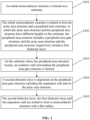
- FIG. 2 is a diagrammatic cross-section of the initial semiconductor structure according to an embodiment of the disclosure.
- the initial semiconductor structure 200 is formed on the substrate 20.
- the substrate 20 is divided into an array area 21, an NMOS thin peripheral area 22, a PMOS thin peripheral area 23, an NMOS thick peripheral area 24 and a PMOS thick peripheral area 25.
- the initial semiconductor structure on the array area 21 includes a third dielectric layer 211, a conductive layer 212 and a first dielectric layer 213.
- the initial semiconductor structure on the NMOS thin peripheral area 22 includes a gate oxide layer 221, a high-k material layer 222, a conductive layer 223 and a first dielectric layer 224.
- the structures or the materials of the conductive layers 212, 223, 235, 243, and 254 in different areas may be different, which will also result in differences of heights of the initial semiconductor structures in different areas.
- the operation that the initial semiconductor structure 200 is formed on the substrate 20 by a semiconductor device may be completed through the following processes.
- the second dielectric layers, the first dielectric layers and the isolation wall are etched to form a semiconductor structure with a flat surface.
- thinning processing to the second dielectric layers is also performed in a semiconductor device to reduce the thickness of the second dielectric layer.
- the thinning processing is completed with a chemical mechanical polishing (CMP) process, which makes the surface of the second dielectric layer flatter.
- CMP chemical mechanical polishing
- FIG. 9 is a diagrammatic cross-section after the thinning processing on the basis of FIG. 6 . Taking FIG. 9 as an example, the thicknesses of the second dielectric layers 611, 621, 631, 641 and 651 is reduced in FIG. 9 compared with FIG. 6 .
- the mask layer may be formed on the initial semiconductor structure first.
- the mask layer is configured to cooperate with the formation of the photoresist layer, such as increasing the adhesion of photoresist and preventing photoresist from penetrating downward.
- the patterned photoresist layer is formed on the mask layer.
- the patterned photoresist layer on the mask layer may be formed by a photo masking process by a semiconductor device.
- the photoresist layer is patterned and includes all desired pattern information of the semiconductor structures to be formed in subsequent processes, so that the needed semiconductor structure can be manufactured in subsequent processes.
- the second dielectric layer, the first dielectric layer and the isolation wall are etched at an etching rate ratio of silicon oxide to silicon nitride.
- the first gas includes carbon tetrafluoride, and the first flow rate is 80-120 standard milliliter/minute; the second gas includes nitrogen, and the second flow rate is 180-220 standard milliliter/minute; the first pressure is 3-7 torr, the first temperature is 20-50 degrees centigrade and shows a downward trend in the first time, which is 20-40 seconds.
Landscapes
- Engineering & Computer Science (AREA)
- Manufacturing & Machinery (AREA)
- Insulated Gate Type Field-Effect Transistor (AREA)
- Element Separation (AREA)
Claims (9)
- Procédé de préparation d'une structure semi-conductrice, comprenant :former une structure semi-conductrice initiale (200) sur un substrat (20) ;graver la structure semi-conductrice initiale (200) pour former une structure de zone de réseau (411) et une structure de zone périphérique, des hauteurs de la structure de zone de réseau (411) et de la structure de zone périphérique sur le substrat (20) étant différentes, la structure de zone périphérique comprenant une structure de grille de zone périphérique (400), et la structure de zone de réseau (411) et la structure de zone périphérique comprenant respectivement une première couche diélectrique (213, 224, 236, 244, 255), un matériau de la première couche diélectrique (213, 224, 236, 244, 255) comprenant du nitrure de silicium ;former une paroi d'isolation entourant la structure de grille de zone périphérique (400) sur le substrat où se trouve la structure de zone périphérique, lorsque la paroi d'isolation comprend une structure de nitrure de silicium-oxyde de silicium-nitrure de silicium ;déposer une deuxième couche diélectrique (611, 621, 631, 641, 651) sur la structure de grille de zone périphérique (400) comprenant la paroi d'isolation et sur la structure de zone de réseau (411), un matériau de la deuxième couche diélectrique (611, 621, 631, 641, 651) comprenant de l'oxyde de silicium ;caractérisé en l'exécution d'un traitement d'amincissement de la deuxième couche diélectrique (611, 621, 631, 641, 651) pour réduire une épaisseur de la deuxième couche diélectrique (611, 621, 631, 641, 651) en utilisant un procédé de polissage mécanique chimique ;graver ultérieurement la deuxième couche diélectrique (611, 621, 631, 641, 651), la première couche diélectrique (213, 224, 236, 244, 255) et la paroi d'isolation avec un rapport de vitesse de gravure d'oxyde de silicium à nitrure de silicium, dans lequel le rapport de vitesse de gravure est de 1: 1 pour former la structure semi-conductrice avec une surface plane.
- Procédé de la revendication 1, dans lequel la gravure de la structure semi-conductrice initiale (200) pour former la structure de zone de réseau (411) et la structure de zone périphérique comprend :former une couche de masque (31, 321, 331, 341, 351) sur la structure semi-conductrice initiale (200) ;former une couche de résine photosensible (312, 322, 332, 342, 352) structurée sur la couche de masque ; etgraver la couche de masque (31, 321, 331, 341,351) sur la base de la couche de résine photosensible (312, 322, 332, 342, 352) structurée pour former la structure de zone de réseau (411) et la structure de zone périphérique.
- Procédé de la revendication 1, dans lequel la structure de grille de zone périphérique (400) comprend au moins une première structure NMOS (421), une première structure PMOS (431), une deuxième structure NMOS (441) et une deuxième structure PMOS (451) ; et
des hauteurs de la structure de zone de réseau (411), de la première structure NMOS (421), de la première structure PMOS (431), de la deuxième structure NMOS (441) et de la deuxième structure PMOS (451) sur le substrat (20) sont différentes. - Procédé de la revendication 3, dans lequel la gravure de la deuxième couche diélectrique (611, 621, 631, 641, 651), de la première couche diélectrique (213, 224, 236, 244, 255) et de la paroi d'isolation pour former la structure semi-conductrice avec une surface plane comprend :
prendre une hauteur la plus basse sur le substrat parmi des hauteurs de la structure de zone de réseau (411), de la première structure NMOS (421) comprenant la paroi d'isolation, de la première structure PMOS (431) comprenant la paroi d'isolation, de la deuxième structure NMOS (441) comprenant la paroi d'isolation et de la deuxième structure PMOS (451) comprenant la paroi d'isolation en tant que point final de gravure pour former la structure semi-conductrice avec une surface plane. - Procédé de la revendication 1, dans lequel la gravure de la deuxième couche diélectrique (611, 621, 631, 641, 651), de la première couche diélectrique (213, 224, 236, 244, 255) et de la paroi d'isolation pour former la structure semi-conductrice avec une surface plane comprend en outre :
prendre une surface de la première couche diélectrique (213, 224, 236, 244, 255) dans la structure de zone de réseau (411) comme point final de gravure pour former la structure semi-conductrice avec une surface plane. - Procédé de la revendication 1, dans lequel la gravure de la deuxième couche diélectrique (611, 621, 631, 641, 651), de la première couche diélectrique (213, 224, 236, 244, 255) et de la paroi d'isolation avec le rapport de vitesse de gravure d'oxyde de silicium sur nitrure de silicium comprend :graver la deuxième couche diélectrique (611, 621, 631, 641, 651), la première couche diélectrique (213, 224, 236, 244, 255) et la paroi d'isolation pendant une première durée dans un environnement d'une première pression et d'une première température en utilisant un gaz de gravure comprenant un premier gaz et un deuxième gaz ;dans lequel le premier gaz est introduit dans une chambre de réaction à un premier débit, et le deuxième gaz est introduit dans la chambre de réaction à un deuxième débit,de préférence dans lequelle premier gaz comprend du tétrafluorure de carbone, et le premier débit est de 80-120 millilitres standard/minute ;le deuxième gaz comprend de l'azote, et le deuxième débit est de 180-220 millilitres standard/minute ;la première pression est de 3-7 torr ;la première température est de 20 à 50 degrés centigrades et la première température diminue pendant la première durée ; etla première durée est de 20 à 40 secondes.
- Procédé de la revendication 3, dans lequella structure de zone de réseau (411) comprend en outre une troisième couche diélectrique (211) ;la structure de zone périphérique comprend en outre une couche high-k (222, 233, 242, 252) et une couche d'oxyde de grille (221, 232, 241, 251) ; etla structure de zone de réseau (411) et la structure de zone périphérique comprennent en outre respectivement une couche conductrice (212, 223, 235, 243, 254).
- Procédé de la revendication 7, dans lequel la première structure PMOS (431) comprend en outre une couche de fonction de travail (234) et une couche tendue (231), et la deuxième structure PMOS (451) comprend en outre une couche de fonction de travail (253),
de préférence dans lequelun matériau de la couche conductrice (212, 223, 235, 243, 254) comprend du tungstène, du nitrure de titane, du polysilicium ou de l'oxyde de lanthane ;un matériau de la troisième couche diélectrique (211) comprend du nitrure de silicium ;un matériau de la couche d'oxyde de grille (221, 232, 241, 251) comprend de l'oxyde de silicium ;un matériau de la couche de fonction de travail (234, 253) comprend de l'alumine ; etun matériau de la couche tendue (231) comprend du silicium-germanium. - Procédé de la revendication 1, dans lequella première couche diélectrique (213, 224, 236, 244, 255) est déposée par un processus de traitement thermique ; etla deuxième couche diélectrique (611, 621, 631, 641, 651) est une couche diélectrique de revêtement par centrifugation.
Applications Claiming Priority (2)
| Application Number | Priority Date | Filing Date | Title |
|---|---|---|---|
| CN202110853063.1A CN115692321B (zh) | 2021-07-27 | 2021-07-27 | 一种半导体结构的制备方法、半导体结构和半导体存储器 |
| PCT/CN2021/112845 WO2023004893A1 (fr) | 2021-07-27 | 2021-08-16 | Procédé de préparation de structure semi-conductrice, structure semi-conductrice et mémoire semi-conductrice |
Publications (3)
| Publication Number | Publication Date |
|---|---|
| EP4177934A1 EP4177934A1 (fr) | 2023-05-10 |
| EP4177934A4 EP4177934A4 (fr) | 2024-02-28 |
| EP4177934B1 true EP4177934B1 (fr) | 2025-04-02 |
Family
ID=85039374
Family Applications (1)
| Application Number | Title | Priority Date | Filing Date |
|---|---|---|---|
| EP21948687.5A Active EP4177934B1 (fr) | 2021-07-27 | 2021-08-16 | Procédé de préparation de structure semi-conductrice, structure semi-conductrice et mémoire semi-conductrice |
Country Status (2)
| Country | Link |
|---|---|
| US (1) | US12262525B2 (fr) |
| EP (1) | EP4177934B1 (fr) |
Family Cites Families (13)
| Publication number | Priority date | Publication date | Assignee | Title |
|---|---|---|---|---|
| US6355524B1 (en) * | 2000-08-15 | 2002-03-12 | Mosel Vitelic, Inc. | Nonvolatile memory structures and fabrication methods |
| US8822287B2 (en) | 2010-12-10 | 2014-09-02 | Samsung Electronics Co., Ltd. | Methods of manufacturing semiconductor devices |
| JP2013051250A (ja) * | 2011-08-30 | 2013-03-14 | Elpida Memory Inc | 半導体装置及びその製造方法 |
| CN103390625B (zh) | 2012-05-10 | 2016-03-23 | 台湾积体电路制造股份有限公司 | 用于bsi图像传感器的背面结构和方法 |
| US8709854B2 (en) | 2012-05-10 | 2014-04-29 | Taiwan Semiconductor Manufacturing Company, Ltd. | Backside structure and methods for BSI image sensors |
| JP6029989B2 (ja) | 2013-01-25 | 2016-11-24 | ルネサスエレクトロニクス株式会社 | 半導体装置の製造方法 |
| KR20140108982A (ko) * | 2013-03-04 | 2014-09-15 | 삼성전자주식회사 | 메모리 장치 및 그 제조 방법 |
| US9812569B2 (en) * | 2014-01-15 | 2017-11-07 | Taiwan Semiconductor Manufacturing Co., Ltd. | Semiconductor device and fabricating method thereof |
| JP5861069B2 (ja) * | 2014-03-27 | 2016-02-16 | パナソニックIpマネジメント株式会社 | 可搬型決済端末装置 |
| US9425206B2 (en) | 2014-12-23 | 2016-08-23 | Taiwan Semiconductor Manufacturing Co., Ltd. | Boundary scheme for embedded poly-SiON CMOS or NVM in HKMG CMOS technology |
| CN108598081B (zh) | 2018-04-25 | 2019-12-10 | 长江存储科技有限责任公司 | 三维存储器件及其制造方法 |
| CN111968911A (zh) | 2020-08-26 | 2020-11-20 | 上海华虹宏力半导体制造有限公司 | 铜制程平坦化的方法 |
| CN111968985B (zh) | 2020-08-26 | 2023-08-15 | 长江存储科技有限责任公司 | 三维存储器的制造方法 |
-
2021
- 2021-08-16 EP EP21948687.5A patent/EP4177934B1/fr active Active
-
2022
- 2022-02-10 US US17/668,661 patent/US12262525B2/en active Active
Also Published As
| Publication number | Publication date |
|---|---|
| EP4177934A4 (fr) | 2024-02-28 |
| EP4177934A1 (fr) | 2023-05-10 |
| US20230031509A1 (en) | 2023-02-02 |
| US12262525B2 (en) | 2025-03-25 |
Similar Documents
| Publication | Publication Date | Title |
|---|---|---|
| US6780708B1 (en) | Method of forming core and periphery gates including two critical masking steps to form a hard mask in a core region that includes a critical dimension less than achievable at a resolution limit of lithography | |
| US8637406B1 (en) | Image transfer process employing a hard mask layer | |
| CN103227101B (zh) | 半导体器件及其制造方法 | |
| JP5105824B2 (ja) | マスク構造物の形成方法及びこれを利用した微細パターン形成方法 | |
| WO2023104455A1 (fr) | Métal à fonction de travail multicouche dans des empilements de nanofeuilles utilisant un matériau d'oxyde sacrificiel | |
| EP4177934B1 (fr) | Procédé de préparation de structure semi-conductrice, structure semi-conductrice et mémoire semi-conductrice | |
| US20070048920A1 (en) | Methods for dual metal gate CMOS integration | |
| US11450659B2 (en) | On-chip decoupling capacitor | |
| KR100728959B1 (ko) | 반도체 소자의 캐패시터 형성방법 | |
| US20080113515A1 (en) | Methods of Forming Semiconductor Devices | |
| US12034034B2 (en) | Method of manufacturing capacitor array | |
| CN115692321B (zh) | 一种半导体结构的制备方法、半导体结构和半导体存储器 | |
| JP7801500B2 (ja) | Dramのキャパシタモールドパターニング用炭化ルテニウム | |
| US6365487B2 (en) | Method of manufacturing a capacitor in a semiconductor device | |
| US20130285202A1 (en) | Semiconductor device | |
| US12080561B2 (en) | Method of processing substrate | |
| US7037777B2 (en) | Process for producing an etching mask on a microstructure, in particular a semiconductor structure with trench capacitors, and corresponding use of the etching mask | |
| US12506033B2 (en) | Method of manufacturing semiconductor device | |
| US20120012979A1 (en) | Semiconductor capacitor | |
| US12094720B2 (en) | Semiconductor structure and manufacturing method thereof | |
| CN112825300A (zh) | 半导体器件及其制备方法 | |
| US20250287562A1 (en) | Semiconductor structure having dielectric liner and method of manufacturing the same | |
| KR20060016269A (ko) | 금속 실리사이드막 형성 방법 및 이를 이용한 반도체소자의 금속배선 형성 방법 | |
| KR20260025076A (ko) | 고종횡비(har) 특징부의 증착 방법 | |
| CN121751736A (zh) | 半导体器件的制备方法 |
Legal Events
| Date | Code | Title | Description |
|---|---|---|---|
| STAA | Information on the status of an ep patent application or granted ep patent |
Free format text: STATUS: UNKNOWN |
|
| STAA | Information on the status of an ep patent application or granted ep patent |
Free format text: STATUS: THE INTERNATIONAL PUBLICATION HAS BEEN MADE |
|
| PUAI | Public reference made under article 153(3) epc to a published international application that has entered the european phase |
Free format text: ORIGINAL CODE: 0009012 |
|
| STAA | Information on the status of an ep patent application or granted ep patent |
Free format text: STATUS: REQUEST FOR EXAMINATION WAS MADE |
|
| 17P | Request for examination filed |
Effective date: 20230110 |
|
| AK | Designated contracting states |
Kind code of ref document: A1 Designated state(s): AL AT BE BG CH CY CZ DE DK EE ES FI FR GB GR HR HU IE IS IT LI LT LU LV MC MK MT NL NO PL PT RO RS SE SI SK SM TR |
|
| REG | Reference to a national code |
Ref country code: DE Ref legal event code: R079 Free format text: PREVIOUS MAIN CLASS: H01L0021320500 Ipc: H01L0021311000 Ref country code: DE Ref legal event code: R079 Ref document number: 602021028715 Country of ref document: DE Free format text: PREVIOUS MAIN CLASS: H01L0021320500 Ipc: H01L0021311000 |
|
| A4 | Supplementary search report drawn up and despatched |
Effective date: 20240129 |
|
| RIC1 | Information provided on ipc code assigned before grant |
Ipc: H01L 27/092 20060101ALI20240123BHEP Ipc: H01L 27/088 20060101ALI20240123BHEP Ipc: H01L 21/8238 20060101ALI20240123BHEP Ipc: H01L 21/8234 20060101ALI20240123BHEP Ipc: H10B 12/00 20230101ALI20240123BHEP Ipc: H01L 21/311 20060101AFI20240123BHEP |
|
| DAV | Request for validation of the european patent (deleted) | ||
| DAX | Request for extension of the european patent (deleted) | ||
| GRAP | Despatch of communication of intention to grant a patent |
Free format text: ORIGINAL CODE: EPIDOSNIGR1 |
|
| STAA | Information on the status of an ep patent application or granted ep patent |
Free format text: STATUS: GRANT OF PATENT IS INTENDED |
|
| INTG | Intention to grant announced |
Effective date: 20241204 |
|
| P01 | Opt-out of the competence of the unified patent court (upc) registered |
Free format text: CASE NUMBER: APP_1889/2025 Effective date: 20250111 |
|
| GRAS | Grant fee paid |
Free format text: ORIGINAL CODE: EPIDOSNIGR3 |
|
| GRAA | (expected) grant |
Free format text: ORIGINAL CODE: 0009210 |
|
| STAA | Information on the status of an ep patent application or granted ep patent |
Free format text: STATUS: THE PATENT HAS BEEN GRANTED |
|
| AK | Designated contracting states |
Kind code of ref document: B1 Designated state(s): AL AT BE BG CH CY CZ DE DK EE ES FI FR GB GR HR HU IE IS IT LI LT LU LV MC MK MT NL NO PL PT RO RS SE SI SK SM TR |
|
| REG | Reference to a national code |
Ref country code: GB Ref legal event code: FG4D |
|
| REG | Reference to a national code |
Ref country code: CH Ref legal event code: EP |
|
| REG | Reference to a national code |
Ref country code: IE Ref legal event code: FG4D |
|
| REG | Reference to a national code |
Ref country code: DE Ref legal event code: R096 Ref document number: 602021028715 Country of ref document: DE |
|
| REG | Reference to a national code |
Ref country code: NL Ref legal event code: MP Effective date: 20250402 |
|
| PG25 | Lapsed in a contracting state [announced via postgrant information from national office to epo] |
Ref country code: NL Free format text: LAPSE BECAUSE OF FAILURE TO SUBMIT A TRANSLATION OF THE DESCRIPTION OR TO PAY THE FEE WITHIN THE PRESCRIBED TIME-LIMIT Effective date: 20250402 |
|
| REG | Reference to a national code |
Ref country code: AT Ref legal event code: MK05 Ref document number: 1782174 Country of ref document: AT Kind code of ref document: T Effective date: 20250402 |
|
| PG25 | Lapsed in a contracting state [announced via postgrant information from national office to epo] |
Ref country code: FI Free format text: LAPSE BECAUSE OF FAILURE TO SUBMIT A TRANSLATION OF THE DESCRIPTION OR TO PAY THE FEE WITHIN THE PRESCRIBED TIME-LIMIT Effective date: 20250402 Ref country code: ES Free format text: LAPSE BECAUSE OF FAILURE TO SUBMIT A TRANSLATION OF THE DESCRIPTION OR TO PAY THE FEE WITHIN THE PRESCRIBED TIME-LIMIT Effective date: 20250402 Ref country code: PT Free format text: LAPSE BECAUSE OF FAILURE TO SUBMIT A TRANSLATION OF THE DESCRIPTION OR TO PAY THE FEE WITHIN THE PRESCRIBED TIME-LIMIT Effective date: 20250804 |
|
| PGFP | Annual fee paid to national office [announced via postgrant information from national office to epo] |
Ref country code: DE Payment date: 20250820 Year of fee payment: 5 |
|
| REG | Reference to a national code |
Ref country code: LT Ref legal event code: MG9D |
|
| PG25 | Lapsed in a contracting state [announced via postgrant information from national office to epo] |
Ref country code: GR Free format text: LAPSE BECAUSE OF FAILURE TO SUBMIT A TRANSLATION OF THE DESCRIPTION OR TO PAY THE FEE WITHIN THE PRESCRIBED TIME-LIMIT Effective date: 20250703 Ref country code: NO Free format text: LAPSE BECAUSE OF FAILURE TO SUBMIT A TRANSLATION OF THE DESCRIPTION OR TO PAY THE FEE WITHIN THE PRESCRIBED TIME-LIMIT Effective date: 20250702 |
|
| PG25 | Lapsed in a contracting state [announced via postgrant information from national office to epo] |
Ref country code: PL Free format text: LAPSE BECAUSE OF FAILURE TO SUBMIT A TRANSLATION OF THE DESCRIPTION OR TO PAY THE FEE WITHIN THE PRESCRIBED TIME-LIMIT Effective date: 20250402 |
|
| PG25 | Lapsed in a contracting state [announced via postgrant information from national office to epo] |
Ref country code: BG Free format text: LAPSE BECAUSE OF FAILURE TO SUBMIT A TRANSLATION OF THE DESCRIPTION OR TO PAY THE FEE WITHIN THE PRESCRIBED TIME-LIMIT Effective date: 20250402 |
|
| PGFP | Annual fee paid to national office [announced via postgrant information from national office to epo] |
Ref country code: GB Payment date: 20250820 Year of fee payment: 5 |
|
| PG25 | Lapsed in a contracting state [announced via postgrant information from national office to epo] |
Ref country code: HR Free format text: LAPSE BECAUSE OF FAILURE TO SUBMIT A TRANSLATION OF THE DESCRIPTION OR TO PAY THE FEE WITHIN THE PRESCRIBED TIME-LIMIT Effective date: 20250402 |
|
| PG25 | Lapsed in a contracting state [announced via postgrant information from national office to epo] |
Ref country code: AT Free format text: LAPSE BECAUSE OF FAILURE TO SUBMIT A TRANSLATION OF THE DESCRIPTION OR TO PAY THE FEE WITHIN THE PRESCRIBED TIME-LIMIT Effective date: 20250402 |
|
| PG25 | Lapsed in a contracting state [announced via postgrant information from national office to epo] |
Ref country code: RS Free format text: LAPSE BECAUSE OF FAILURE TO SUBMIT A TRANSLATION OF THE DESCRIPTION OR TO PAY THE FEE WITHIN THE PRESCRIBED TIME-LIMIT Effective date: 20250702 |
|
| PG25 | Lapsed in a contracting state [announced via postgrant information from national office to epo] |
Ref country code: IS Free format text: LAPSE BECAUSE OF FAILURE TO SUBMIT A TRANSLATION OF THE DESCRIPTION OR TO PAY THE FEE WITHIN THE PRESCRIBED TIME-LIMIT Effective date: 20250802 |
|
| PG25 | Lapsed in a contracting state [announced via postgrant information from national office to epo] |
Ref country code: LV Free format text: LAPSE BECAUSE OF FAILURE TO SUBMIT A TRANSLATION OF THE DESCRIPTION OR TO PAY THE FEE WITHIN THE PRESCRIBED TIME-LIMIT Effective date: 20250402 |
|
| REG | Reference to a national code |
Ref country code: DE Ref legal event code: R097 Ref document number: 602021028715 Country of ref document: DE |
|
| PG25 | Lapsed in a contracting state [announced via postgrant information from national office to epo] |
Ref country code: SM Free format text: LAPSE BECAUSE OF FAILURE TO SUBMIT A TRANSLATION OF THE DESCRIPTION OR TO PAY THE FEE WITHIN THE PRESCRIBED TIME-LIMIT Effective date: 20250402 Ref country code: DK Free format text: LAPSE BECAUSE OF FAILURE TO SUBMIT A TRANSLATION OF THE DESCRIPTION OR TO PAY THE FEE WITHIN THE PRESCRIBED TIME-LIMIT Effective date: 20250402 |
|
| PG25 | Lapsed in a contracting state [announced via postgrant information from national office to epo] |
Ref country code: CZ Free format text: LAPSE BECAUSE OF FAILURE TO SUBMIT A TRANSLATION OF THE DESCRIPTION OR TO PAY THE FEE WITHIN THE PRESCRIBED TIME-LIMIT Effective date: 20250402 |
|
| PG25 | Lapsed in a contracting state [announced via postgrant information from national office to epo] |
Ref country code: EE Free format text: LAPSE BECAUSE OF FAILURE TO SUBMIT A TRANSLATION OF THE DESCRIPTION OR TO PAY THE FEE WITHIN THE PRESCRIBED TIME-LIMIT Effective date: 20250402 |
|
| PG25 | Lapsed in a contracting state [announced via postgrant information from national office to epo] |
Ref country code: SK Free format text: LAPSE BECAUSE OF FAILURE TO SUBMIT A TRANSLATION OF THE DESCRIPTION OR TO PAY THE FEE WITHIN THE PRESCRIBED TIME-LIMIT Effective date: 20250402 |
|
| PG25 | Lapsed in a contracting state [announced via postgrant information from national office to epo] |
Ref country code: IT Free format text: LAPSE BECAUSE OF FAILURE TO SUBMIT A TRANSLATION OF THE DESCRIPTION OR TO PAY THE FEE WITHIN THE PRESCRIBED TIME-LIMIT Effective date: 20250402 |
|
| PLBE | No opposition filed within time limit |
Free format text: ORIGINAL CODE: 0009261 |
|
| STAA | Information on the status of an ep patent application or granted ep patent |
Free format text: STATUS: NO OPPOSITION FILED WITHIN TIME LIMIT |
|
| REG | Reference to a national code |
Ref country code: CH Ref legal event code: L10 Free format text: ST27 STATUS EVENT CODE: U-0-0-L10-L00 (AS PROVIDED BY THE NATIONAL OFFICE) Effective date: 20260211 |
|
| PG25 | Lapsed in a contracting state [announced via postgrant information from national office to epo] |
Ref country code: RO Free format text: LAPSE BECAUSE OF FAILURE TO SUBMIT A TRANSLATION OF THE DESCRIPTION OR TO PAY THE FEE WITHIN THE PRESCRIBED TIME-LIMIT Effective date: 20250402 |
|
| 26N | No opposition filed |
Effective date: 20260105 |
|
| REG | Reference to a national code |
Ref country code: CH Ref legal event code: H13 Free format text: ST27 STATUS EVENT CODE: U-0-0-H10-H13 (AS PROVIDED BY THE NATIONAL OFFICE) Effective date: 20260324 |
|
| PG25 | Lapsed in a contracting state [announced via postgrant information from national office to epo] |
Ref country code: MC Free format text: LAPSE BECAUSE OF FAILURE TO SUBMIT A TRANSLATION OF THE DESCRIPTION OR TO PAY THE FEE WITHIN THE PRESCRIBED TIME-LIMIT Effective date: 20250402 |
|
| PG25 | Lapsed in a contracting state [announced via postgrant information from national office to epo] |
Ref country code: LU Free format text: LAPSE BECAUSE OF NON-PAYMENT OF DUE FEES Effective date: 20250816 |
|
| PG25 | Lapsed in a contracting state [announced via postgrant information from national office to epo] |
Ref country code: CH Free format text: LAPSE BECAUSE OF NON-PAYMENT OF DUE FEES Effective date: 20250831 |