EP4202141A1 - Funkwellenabsorber - Google Patents
Funkwellenabsorber Download PDFInfo
- Publication number
- EP4202141A1 EP4202141A1 EP21861386.7A EP21861386A EP4202141A1 EP 4202141 A1 EP4202141 A1 EP 4202141A1 EP 21861386 A EP21861386 A EP 21861386A EP 4202141 A1 EP4202141 A1 EP 4202141A1
- Authority
- EP
- European Patent Office
- Prior art keywords
- radio wave
- dielectric layer
- layer
- wave absorber
- absorber according
- Prior art date
- Legal status (The legal status is an assumption and is not a legal conclusion. Google has not performed a legal analysis and makes no representation as to the accuracy of the status listed.)
- Pending
Links
Images


Classifications
-
- H—ELECTRICITY
- H05—ELECTRIC TECHNIQUES NOT OTHERWISE PROVIDED FOR
- H05K—PRINTED CIRCUITS; CASINGS OR CONSTRUCTIONAL DETAILS OF ELECTRIC APPARATUS; MANUFACTURE OF ASSEMBLAGES OF ELECTRICAL COMPONENTS
- H05K9/00—Screening of apparatus or components against electric or magnetic fields
- H05K9/0073—Shielding materials
- H05K9/0094—Shielding materials being light-transmitting, e.g. transparent, translucent
-
- B—PERFORMING OPERATIONS; TRANSPORTING
- B32—LAYERED PRODUCTS
- B32B—LAYERED PRODUCTS, i.e. PRODUCTS BUILT-UP OF STRATA OF FLAT OR NON-FLAT, e.g. CELLULAR OR HONEYCOMB, FORM
- B32B17/00—Layered products essentially comprising sheet glass, or glass, slag, or like fibres
- B32B17/06—Layered products essentially comprising sheet glass, or glass, slag, or like fibres comprising glass as the main or only constituent of a layer, next to another layer of a specific material
- B32B17/10—Layered products essentially comprising sheet glass, or glass, slag, or like fibres comprising glass as the main or only constituent of a layer, next to another layer of a specific material of synthetic resin
- B32B17/10005—Layered products essentially comprising sheet glass, or glass, slag, or like fibres comprising glass as the main or only constituent of a layer, next to another layer of a specific material of synthetic resin laminated safety glass or glazing
- B32B17/10009—Layered products essentially comprising sheet glass, or glass, slag, or like fibres comprising glass as the main or only constituent of a layer, next to another layer of a specific material of synthetic resin laminated safety glass or glazing characterized by the number, the constitution or treatment of glass sheets
- B32B17/10036—Layered products essentially comprising sheet glass, or glass, slag, or like fibres comprising glass as the main or only constituent of a layer, next to another layer of a specific material of synthetic resin laminated safety glass or glazing characterized by the number, the constitution or treatment of glass sheets comprising two outer glass sheets
-
- B—PERFORMING OPERATIONS; TRANSPORTING
- B32—LAYERED PRODUCTS
- B32B—LAYERED PRODUCTS, i.e. PRODUCTS BUILT-UP OF STRATA OF FLAT OR NON-FLAT, e.g. CELLULAR OR HONEYCOMB, FORM
- B32B17/00—Layered products essentially comprising sheet glass, or glass, slag, or like fibres
- B32B17/06—Layered products essentially comprising sheet glass, or glass, slag, or like fibres comprising glass as the main or only constituent of a layer, next to another layer of a specific material
- B32B17/10—Layered products essentially comprising sheet glass, or glass, slag, or like fibres comprising glass as the main or only constituent of a layer, next to another layer of a specific material of synthetic resin
- B32B17/10005—Layered products essentially comprising sheet glass, or glass, slag, or like fibres comprising glass as the main or only constituent of a layer, next to another layer of a specific material of synthetic resin laminated safety glass or glazing
- B32B17/10165—Functional features of the laminated safety glass or glazing
- B32B17/10174—Coatings of a metallic or dielectric material on a constituent layer of glass or polymer
- B32B17/10183—Coatings of a metallic or dielectric material on a constituent layer of glass or polymer being not continuous, e.g. in edge regions
-
- B—PERFORMING OPERATIONS; TRANSPORTING
- B32—LAYERED PRODUCTS
- B32B—LAYERED PRODUCTS, i.e. PRODUCTS BUILT-UP OF STRATA OF FLAT OR NON-FLAT, e.g. CELLULAR OR HONEYCOMB, FORM
- B32B17/00—Layered products essentially comprising sheet glass, or glass, slag, or like fibres
- B32B17/06—Layered products essentially comprising sheet glass, or glass, slag, or like fibres comprising glass as the main or only constituent of a layer, next to another layer of a specific material
- B32B17/10—Layered products essentially comprising sheet glass, or glass, slag, or like fibres comprising glass as the main or only constituent of a layer, next to another layer of a specific material of synthetic resin
- B32B17/10005—Layered products essentially comprising sheet glass, or glass, slag, or like fibres comprising glass as the main or only constituent of a layer, next to another layer of a specific material of synthetic resin laminated safety glass or glazing
- B32B17/10165—Functional features of the laminated safety glass or glazing
- B32B17/10174—Coatings of a metallic or dielectric material on a constituent layer of glass or polymer
- B32B17/10201—Dielectric coatings
-
- B—PERFORMING OPERATIONS; TRANSPORTING
- B32—LAYERED PRODUCTS
- B32B—LAYERED PRODUCTS, i.e. PRODUCTS BUILT-UP OF STRATA OF FLAT OR NON-FLAT, e.g. CELLULAR OR HONEYCOMB, FORM
- B32B17/00—Layered products essentially comprising sheet glass, or glass, slag, or like fibres
- B32B17/06—Layered products essentially comprising sheet glass, or glass, slag, or like fibres comprising glass as the main or only constituent of a layer, next to another layer of a specific material
- B32B17/10—Layered products essentially comprising sheet glass, or glass, slag, or like fibres comprising glass as the main or only constituent of a layer, next to another layer of a specific material of synthetic resin
- B32B17/10005—Layered products essentially comprising sheet glass, or glass, slag, or like fibres comprising glass as the main or only constituent of a layer, next to another layer of a specific material of synthetic resin laminated safety glass or glazing
- B32B17/10165—Functional features of the laminated safety glass or glazing
- B32B17/10174—Coatings of a metallic or dielectric material on a constituent layer of glass or polymer
- B32B17/1022—Metallic coatings
-
- B—PERFORMING OPERATIONS; TRANSPORTING
- B32—LAYERED PRODUCTS
- B32B—LAYERED PRODUCTS, i.e. PRODUCTS BUILT-UP OF STRATA OF FLAT OR NON-FLAT, e.g. CELLULAR OR HONEYCOMB, FORM
- B32B17/00—Layered products essentially comprising sheet glass, or glass, slag, or like fibres
- B32B17/06—Layered products essentially comprising sheet glass, or glass, slag, or like fibres comprising glass as the main or only constituent of a layer, next to another layer of a specific material
- B32B17/10—Layered products essentially comprising sheet glass, or glass, slag, or like fibres comprising glass as the main or only constituent of a layer, next to another layer of a specific material of synthetic resin
- B32B17/10005—Layered products essentially comprising sheet glass, or glass, slag, or like fibres comprising glass as the main or only constituent of a layer, next to another layer of a specific material of synthetic resin laminated safety glass or glazing
- B32B17/10165—Functional features of the laminated safety glass or glazing
- B32B17/10376—Laminated safety glass or glazing containing metal wires
- B32B17/10403—Laminated safety glass or glazing containing metal wires for radiation shielding
-
- H—ELECTRICITY
- H01—ELECTRIC ELEMENTS
- H01Q—ANTENNAS, i.e. RADIO AERIALS
- H01Q17/00—Devices for absorbing waves radiated from an antenna; Combinations of such devices with active antenna elements or systems
-
- H—ELECTRICITY
- H01—ELECTRIC ELEMENTS
- H01Q—ANTENNAS, i.e. RADIO AERIALS
- H01Q17/00—Devices for absorbing waves radiated from an antenna; Combinations of such devices with active antenna elements or systems
- H01Q17/002—Devices for absorbing waves radiated from an antenna; Combinations of such devices with active antenna elements or systems using short elongated elements as dissipative material, e.g. metallic threads or flake-like particles
-
- B—PERFORMING OPERATIONS; TRANSPORTING
- B32—LAYERED PRODUCTS
- B32B—LAYERED PRODUCTS, i.e. PRODUCTS BUILT-UP OF STRATA OF FLAT OR NON-FLAT, e.g. CELLULAR OR HONEYCOMB, FORM
- B32B17/00—Layered products essentially comprising sheet glass, or glass, slag, or like fibres
- B32B17/06—Layered products essentially comprising sheet glass, or glass, slag, or like fibres comprising glass as the main or only constituent of a layer, next to another layer of a specific material
- B32B17/10—Layered products essentially comprising sheet glass, or glass, slag, or like fibres comprising glass as the main or only constituent of a layer, next to another layer of a specific material of synthetic resin
- B32B17/10005—Layered products essentially comprising sheet glass, or glass, slag, or like fibres comprising glass as the main or only constituent of a layer, next to another layer of a specific material of synthetic resin laminated safety glass or glazing
- B32B17/10009—Layered products essentially comprising sheet glass, or glass, slag, or like fibres comprising glass as the main or only constituent of a layer, next to another layer of a specific material of synthetic resin laminated safety glass or glazing characterized by the number, the constitution or treatment of glass sheets
- B32B17/10036—Layered products essentially comprising sheet glass, or glass, slag, or like fibres comprising glass as the main or only constituent of a layer, next to another layer of a specific material of synthetic resin laminated safety glass or glazing characterized by the number, the constitution or treatment of glass sheets comprising two outer glass sheets
- B32B17/10045—Layered products essentially comprising sheet glass, or glass, slag, or like fibres comprising glass as the main or only constituent of a layer, next to another layer of a specific material of synthetic resin laminated safety glass or glazing characterized by the number, the constitution or treatment of glass sheets comprising two outer glass sheets with at least one intermediate layer consisting of a glass sheet
-
- B—PERFORMING OPERATIONS; TRANSPORTING
- B32—LAYERED PRODUCTS
- B32B—LAYERED PRODUCTS, i.e. PRODUCTS BUILT-UP OF STRATA OF FLAT OR NON-FLAT, e.g. CELLULAR OR HONEYCOMB, FORM
- B32B17/00—Layered products essentially comprising sheet glass, or glass, slag, or like fibres
- B32B17/06—Layered products essentially comprising sheet glass, or glass, slag, or like fibres comprising glass as the main or only constituent of a layer, next to another layer of a specific material
- B32B17/10—Layered products essentially comprising sheet glass, or glass, slag, or like fibres comprising glass as the main or only constituent of a layer, next to another layer of a specific material of synthetic resin
- B32B17/10005—Layered products essentially comprising sheet glass, or glass, slag, or like fibres comprising glass as the main or only constituent of a layer, next to another layer of a specific material of synthetic resin laminated safety glass or glazing
- B32B17/1055—Layered products essentially comprising sheet glass, or glass, slag, or like fibres comprising glass as the main or only constituent of a layer, next to another layer of a specific material of synthetic resin laminated safety glass or glazing characterized by the resin layer, i.e. interlayer
- B32B17/10761—Layered products essentially comprising sheet glass, or glass, slag, or like fibres comprising glass as the main or only constituent of a layer, next to another layer of a specific material of synthetic resin laminated safety glass or glazing characterized by the resin layer, i.e. interlayer containing vinyl acetal
-
- B—PERFORMING OPERATIONS; TRANSPORTING
- B32—LAYERED PRODUCTS
- B32B—LAYERED PRODUCTS, i.e. PRODUCTS BUILT-UP OF STRATA OF FLAT OR NON-FLAT, e.g. CELLULAR OR HONEYCOMB, FORM
- B32B17/00—Layered products essentially comprising sheet glass, or glass, slag, or like fibres
- B32B17/06—Layered products essentially comprising sheet glass, or glass, slag, or like fibres comprising glass as the main or only constituent of a layer, next to another layer of a specific material
- B32B17/10—Layered products essentially comprising sheet glass, or glass, slag, or like fibres comprising glass as the main or only constituent of a layer, next to another layer of a specific material of synthetic resin
- B32B17/10005—Layered products essentially comprising sheet glass, or glass, slag, or like fibres comprising glass as the main or only constituent of a layer, next to another layer of a specific material of synthetic resin laminated safety glass or glazing
- B32B17/1055—Layered products essentially comprising sheet glass, or glass, slag, or like fibres comprising glass as the main or only constituent of a layer, next to another layer of a specific material of synthetic resin laminated safety glass or glazing characterized by the resin layer, i.e. interlayer
- B32B17/1077—Layered products essentially comprising sheet glass, or glass, slag, or like fibres comprising glass as the main or only constituent of a layer, next to another layer of a specific material of synthetic resin laminated safety glass or glazing characterized by the resin layer, i.e. interlayer containing polyurethane
-
- B—PERFORMING OPERATIONS; TRANSPORTING
- B32—LAYERED PRODUCTS
- B32B—LAYERED PRODUCTS, i.e. PRODUCTS BUILT-UP OF STRATA OF FLAT OR NON-FLAT, e.g. CELLULAR OR HONEYCOMB, FORM
- B32B17/00—Layered products essentially comprising sheet glass, or glass, slag, or like fibres
- B32B17/06—Layered products essentially comprising sheet glass, or glass, slag, or like fibres comprising glass as the main or only constituent of a layer, next to another layer of a specific material
- B32B17/10—Layered products essentially comprising sheet glass, or glass, slag, or like fibres comprising glass as the main or only constituent of a layer, next to another layer of a specific material of synthetic resin
- B32B17/10005—Layered products essentially comprising sheet glass, or glass, slag, or like fibres comprising glass as the main or only constituent of a layer, next to another layer of a specific material of synthetic resin laminated safety glass or glazing
- B32B17/1055—Layered products essentially comprising sheet glass, or glass, slag, or like fibres comprising glass as the main or only constituent of a layer, next to another layer of a specific material of synthetic resin laminated safety glass or glazing characterized by the resin layer, i.e. interlayer
- B32B17/10788—Layered products essentially comprising sheet glass, or glass, slag, or like fibres comprising glass as the main or only constituent of a layer, next to another layer of a specific material of synthetic resin laminated safety glass or glazing characterized by the resin layer, i.e. interlayer containing ethylene vinylacetate
-
- B—PERFORMING OPERATIONS; TRANSPORTING
- B32—LAYERED PRODUCTS
- B32B—LAYERED PRODUCTS, i.e. PRODUCTS BUILT-UP OF STRATA OF FLAT OR NON-FLAT, e.g. CELLULAR OR HONEYCOMB, FORM
- B32B2307/00—Properties of the layers or laminate
- B32B2307/20—Properties of the layers or laminate having particular electrical or magnetic properties, e.g. piezoelectric
- B32B2307/212—Electromagnetic interference shielding
-
- B—PERFORMING OPERATIONS; TRANSPORTING
- B32—LAYERED PRODUCTS
- B32B—LAYERED PRODUCTS, i.e. PRODUCTS BUILT-UP OF STRATA OF FLAT OR NON-FLAT, e.g. CELLULAR OR HONEYCOMB, FORM
- B32B2307/00—Properties of the layers or laminate
- B32B2307/70—Other properties
- B32B2307/732—Dimensional properties
- B32B2307/737—Dimensions, e.g. volume or area
- B32B2307/7375—Linear, e.g. length, distance or width
-
- B—PERFORMING OPERATIONS; TRANSPORTING
- B32—LAYERED PRODUCTS
- B32B—LAYERED PRODUCTS, i.e. PRODUCTS BUILT-UP OF STRATA OF FLAT OR NON-FLAT, e.g. CELLULAR OR HONEYCOMB, FORM
- B32B27/00—Layered products comprising a layer of synthetic resin
- B32B27/36—Layered products comprising a layer of synthetic resin comprising polyesters
- B32B27/365—Layered products comprising a layer of synthetic resin comprising polyesters comprising polycarbonates
-
- E—FIXED CONSTRUCTIONS
- E04—BUILDING
- E04B—GENERAL BUILDING CONSTRUCTIONS; WALLS, e.g. PARTITIONS; ROOFS; FLOORS; CEILINGS; INSULATION OR OTHER PROTECTION OF BUILDINGS
- E04B1/00—Constructions in general; Structures which are not restricted either to walls, e.g. partitions, or floors or ceilings or roofs
- E04B1/62—Insulation or other protection; Elements or use of specified material therefor
- E04B1/92—Protection against other undesired influences or dangers
- E04B2001/925—Protection against harmful electro-magnetic or radio-active radiations, e.g. X-rays
Definitions
- the present invention relates to a radio wave absorber.
- the radio wave absorber disclosed in Patent Document 1 is a laminate which absorbs radio waves for wireless LAN and has a light transmittance of 50% or more.
- the radio wave absorber is of ⁇ /4 type and has (A) a glass layer, (B) a PET film, (C) a resistive film, (D) a dielectric layer, (E) a reflective film, (F) a PET film and (G) a glass layer in this order from the radio wave incident direction.
- Patent Document 1 JP-A-2006-86446
- the distance between the resistive film and the reflective film is about ⁇ /4.
- ⁇ is the wavelength of radio waves.
- the resistive film reflects a part of radio waves, absorbs another part and transmits the other part.
- the radio waves reflected on the resistive film and the radio waves reflected on the reflective film interfere with each other and are cancelled out each other. As a result, the radio waves are absorbed.
- the distance between the resistive film and the reflective film is about ⁇ /4. Accordingly, the longer the wavelength ⁇ of radio waves is, that is the lower the frequency of the radio waves is, the thicker the ⁇ /4 radio wave absorber will be.
- a technique to make the radio wave absorber thin is provided.
- the radio wave absorber according to an embodiment of the present invention is a radio wave absorber having a laminate structure
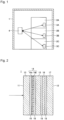
- the radio wave absorber 1 absorbs unnecessary radio waves when radio waves are transmitted/received for example between RF (Radio Frequency) tags 3A, 3B and 3C attached to articles 2A, 2B and 2C, and a reader 4. It can suppress reflection of unnecessary radio waves and prevent e.g. miscounting of the number of the articles 2A, 2B and 2C.
- RF Radio Frequency
- the RF tags 3A, 3B and 3C contain a storage medium which stores information to identify the articles 2A, 2B and 2C.
- the RF tags 3A, 3B and 3C may, for example, be of passive type such that using radio waves emitted from the reader 4 as a power source, they transmit radio waves of information preliminarily stored in the storage medium to the reader 4.
- the frequency of the radio waves emitted from the RF tags 3A, 3B and 3C is for example 913 MHz.
- the RF tags 3A, 3B and 3C are of passive type in the present embodiment, but may be of active type such that they contain a built-in battery as a power source.
- the reader 4 receives radio waves emitted from the RF tags 3A, 3B and 3C, reads information contained in the radio waves and identifies the articles 2A, 2B and 2C.
- the maximum communication distance of the reader 4 is not particularly limited and is for example about 6 m.
- the sum of the articles 2A, 2B and 2C identified by the reader 4 is displayed on a display device.
- the radio wave absorber 1 may, for example, be in a box shape and contains the reader 4 in its interior. A purchaser puts the articles 2A, 2B and 2C for example from outside the radio wave absorber 1 into inside. In such a case, to secure sense of safety for the purchaser, the radio wave absorber 1 may be required to be transparent.
- the radio wave absorber 1 may have a size to such an extent that even a purchaser can enter.
- the purchaser enters into the interior of the radio wave absorber 1 together with the articles 2A, 2B and 2C.
- the radio wave absorber 1 may be required to be transparent so that the purchaser does not feel being trapped.
- the radio wave absorber 1 may sometimes be required to be transparent so that the purchaser can see the article or scenery through the radio wave absorber 1.
- the radio wave absorber 1 is transparent, the interior and the exterior of the radio wave absorber can be visually recognized, and articles in the radio wave absorber 1 can automatically be visually recognized, and thus it can be used for a self checkout or a storehouse.
- a first example of the radio wave absorber 1 will be described with reference to Fig. 2 .
- the direction of incidence of radio waves RF is indicted by an arrow.
- the radio wave absorber 1 has a laminate structure, absorbs radio waves at a specific frequency and has a visible light transmittance of 50% or more.
- the visible light transmittance is preferably 53% or more, more preferably 55% or more. Further, the visible light transmittance is preferably 90% or less, more preferably 80% or less.
- the visible light transmittance is obtained by measurement in accordance with Japanese Industrial Standards JIS R3106:1998 and by calculation by a calculation formula in the case of using standard illuminant D65.
- the radio wave absorber 1 has a first principal surface 11 which the radio waves enter, and a second principal surface 12 on the opposite side from the first principal surface 11.
- the radio wave absorber 1 has, in the following order from the first principal surface 11 toward the second principal surface 12, a first dielectric layer 13, a conductive layer 14, a second dielectric layer 15, a radio wave reflective layer 16 and a third dielectric layer 17.
- the radio wave absorber 1 may further has an adhesive layer 18 between the first principal surface 11 and the second principal surface 12.
- the adhesive layer 18 is disposed at least one of between the first dielectric layer 13 and the conductive layer 14, between the conductive layer 14 and the second dielectric layer 15, between the second dielectric layer 15 and the radio wave reflective layer 16, and between the radio wave reflective layer 16 and the third dielectric layer 17.
- the disposition of the adhesive layer 18 is not particularly limited, the details of which will be described later.
- the first dielectric layer 13 protects the conductive layer 14.
- the first dielectric layer 13 is made of glass, a ceramic, a resin or the like. From the viewpoint of weight saving, a resin is preferred. As specific examples of the resin, a polyethylene terephthalate (PET) resin, a polycarbonate (PC) resin and an acrylic resin may be mentioned. On the other hand, from the viewpoint of scratch resistance, glass or a ceramic is preferred.
- the first dielectric layer 13 is a glass substrate or a ceramic substrate
- its thickness is for example from 0.2 mm to 4.0 mm, preferably from 0.3 mm to 2.5 mm, more preferably from 0.3 mm to 1.0 mm.
- its thickness is for example from 0.4 mm to 5.0 mm, preferably from 0.5 mm to 3.5 mm, more preferably from 0.5 mm to 1.5 mm.
- tan ⁇ (also called dielectric loss tangent) of the glass substrate is preferably 0.025 or less, more preferably 0.020 or less, further preferably 0.010 or less.
- the lower limit of tan ⁇ of the glass substrate is not particularly limited and may be 0.0001 or more.
- the relative dielectric constant of the glass substrate is preferably 8 or less, more preferably 6 or less.
- the lower limit of the relative dielectric constant of the glass substrate is not particularly limited and may be 3.5 or more.
- tan ⁇ of the resin substrate is preferably 0.2 or less, more preferably 0.1 or less.
- the lower limit of tan ⁇ of the resin substrate is not particularly limited and may be 0.0005 or more.
- the relative dielectric constant of the resin substrate is preferably 5 or less, more preferably 4 or less.
- the lower limit of the relative dielectric constant of the resin substrate is not particularly limited and may be 2 or more.
- tan ⁇ is a value represented by ⁇ 2/ ⁇ 1 employing the complex dielectric constant, and ⁇ 1 is the relative dielectric constant, and ⁇ 2 is the dissipation loss.
- tan ⁇ and the relative dielectric constant are values measured in accordance with the method specified in IEC (International Electrotechnical Commission) 61189-2-721 (2015), at a measurement frequency of 1 GHz.
- the ratio (Ta/Tc) of the thickness (Ta) of the first dielectric layer 13 to the thickness (Tc) of the second dielectric layer 15 is for example from 0.05 to 0.75.
- the first dielectric layer 13 is intended to protect the conductive layer 14 and thereby may be thinner than the second dielectric layer 15.
- the conductive layer 14 contains a plurality of conductors 14a disposed to be separated by gaps, insulated from each other.
- the conductors 14a may, for example, be a transparent conductive film such as an ITO (indium tin oxide) film or a Low-E (low emissivity) film.
- the conductive layer 14 may be a so-called FSS (Frequency Selective Shield).
- the conductive layer 14 reflects a part of radio waves, absorbs another part, and transmit the other part. Radio waves which had transmitted through the conductive layer 14 are reflected on the radio wave reflective layer 16. The radio waves reflected on the conductive layer 14 and the radio waves reflected on the radio wave reflective layer 16 interfere with each other and are cancelled out each other. As a result, the radio waves are absorbed.
- the distance between the conductive layer 14 (resistive film) and the radio wave reflective layer 16 (reflective film) can be made shorter than ⁇ /4 and the radio wave absorber 1 can be made thin.
- the distance between the conductive layer 14 and the radio wave reflective layer 16 is preferably from 1.5 mm to 20 mm, more preferably from 2 mm to 10mm, further preferably from 2 mm to 5 mm.
- the thickness of the conductive layer 14 is not particularly limited and for example in a case where the conductive layer 14 is a Low-E (low emissivity) film, it is from 50 nm to 300 nm.
- the conductive layer 14 may further has an insulating substrate 14b which supports the plurality of conductors 14a.
- the insulating substrate 14b may, for example, be a resin film.
- the plurality of conductors 14a are formed on the surface of the insulating substrate 14b.
- a transparent conductive film is formed on the surface of the insulating substrate 14b e.g. by deposition or sputtering, and the formed transparent conductive film is patterned e.g. by laser processing.
- the plurality of conductors 14a may also be formed by printing using a conductive ink.
- the thickness of the insulating substrate 14b is not particularly limited and may, for example, be from 50 ⁇ m to 200 ⁇ m.
- the adhesive layer 18 is disposed both between the conductive layer 14 and the first dielectric layer 13 and between the conductive layer 14 and the second dielectric layer 15.
- the adhesive layer 18 is disposed only one of between the conductive layer 14 and the first dielectric layer 13 and between the conductive layer 14 and the second dielectric layer 15.
- the conductive layer 14 is adjacent to and is directly formed on one of the first dielectric layer 13 and the second dielectric layer 15.
- the conductive layer 14 is adjacent to the second dielectric layer 15 and is directly formed on the second dielectric layer 15.
- the conductive layer 14 is adjacent to the first dielectric layer 13 and is directly formed on the first dielectric layer 13. Since no insulating substrate 14b is necessary, the radio wave absorber 1 can be made thinner.
- the conductive layer 14 comprises a plurality of conductors 14a and gaps disposed to separate the plurality of conductors 14a, and the plurality of conductors 14a are insulated each other by the gaps.
- the gaps comprise a plurality of first slits 14c and a plurality of second slits 14d orthogonal to each other.
- the plurality of first slits 14c and the plurality of second slits 14d form quadrangular lattices, and the conductors 14a are formed rectangular as viewed two-dimensionally.
- the rectangular includes square.
- first slits 14c are set alternately to first distances L1 and second distances L2 narrower than the first distances L1.
- second slits 14d are also set alternately to first distances L1 and second distances L2.
- conductors 14a-1, 14a-2, 14a-3 and 14a-4 are formed as viewed two-dimensionally.
- the conductor 14a-1 is a square with lengths of the four sides being L1.
- the conductor 14a-2 is a square with lengths of the four sides being L2.
- the other two conductors 14a-3 and 14a-4 have lengths of facing two sides being L1 and lengths of the other two sides being L2.
- the average of the lengths of the outer peripheries of the four types of conductors 14a-1, 14a-2, 14a-3 and 14a-4 is represented by the formula 2 ⁇ (L1+L2).
- the average of the lengths of the outer peripheries is for example from 60 mm to 180 mm, preferably from 80 mm to 150 mm.
- L1 and L2 are different in the present embodiment but may be the same.
- the average of the lengths of the outer peripheries is represented by the formula 2 ⁇ (L1+L2).
- the first slit 14c and the second slit 14d are formed for example by laser processing as described above.
- the laser beam forms a spot SP on the surface of the conductive layer 14.
- the longitudinal direction of the first slit 14c is the X axis direction.
- the second slit 14d is formed.
- the longitudinal direction of the second slit 14d is the Y axis direction.
- the line width G1 of the first slit 14c agrees with the size of the spot SP in the Y axis direction
- the line width G2 of the second slit 14d agrees with the size of the spot SP in the X axis direction.
- G1 and G2 are different from each other.
- G1 and G2 agree with each other.
- G1 and G2 agree with each other, it is not necessary to distinguish G1 and G2, and they will be represented simply as G (see Fig. 5 ).
- the radio wave absorber 1 was a 5-layered laminate having the first dielectric layer 13, the conductive layer 14, the second dielectric layer 15, the radio wave reflective layer 16 and the third dielectric layer 17 in this order.
- the laminate was disposed so that the first principal surface 11 stood vertically, the longitudinal direction of the first slits 14c was horizontal, and the longitudinal direction of the second slits 14d was vertical.
- the first dielectric layer 13 and the third dielectric layer 17 were both PC resin substrates (relative dielectric constant: 2.96, tan ⁇ : 0.011) having a thickness of 2.0 mm.
- the second dielectric layer 15 was a glass substrate (relative dielectric constant: 7.0, tan ⁇ : 0.02) having a thickness of 4.0 mm.
- the radio wave reflective layer 16 was a perfect magnetic conductor (PEC).
- the radio wave absorber 1 (manufactured by Microwave Absorbers Inc., product number "MS-009T”) was a 5-layered laminate having the conductive layer 14 comprising the insulating substrate 14b and the conductors 14a, the second dielectric layer 15, and the radio wave reflective layer 16 comprising a tile-shaped layer and a solid film-formed layer in this order.
- the laminate was disposed so that the first principal surface 11 stood vertically, the longitudinal direction of the first slits 14c was horizontal, and the longitudinal direction of the second slits 14d was vertical.
- the second dielectric layer 15 was an acrylic resin (relative dielectric constant: 2.7, tan ⁇ : 0.04) having a thickness of 5.0 mm.
- the conductive layer 14 L1 was 86 mm, L2 was 86 mm, G1 was 4000 ⁇ m, G2 was 4000 ⁇ m, and the sheet resistance was 5.38 ⁇ /sq.
- the tile-shaped layer had a sheet resistance of 3.21 ⁇ /sq.
- the solid film-formed layer had a sheet resistance of 2.64 ⁇ /sq.
- the whole radio wave reflective layer 16 had a sheet resistance of 1.57 ⁇ /sq.
- G1 and G2 are each independently preferably from 30 ⁇ m to 500 ⁇ m, more preferably from 50 ⁇ m to 200 ⁇ m, further preferably from 50 ⁇ m to 150 ⁇ m.
- G1 and G2 are 30 ⁇ m or more, processing will be easy.
- Table 1 when G1 and G2 are 500 ⁇ m or less, the distance between adjacent conductive layers 14 (14a-1, 14a-2, 14a-3, 14a-4) is suppressed, the slits are less likely to be visually recognized, and a radio wave absorber 1 with favorable transparency is thereby obtained.
- G1 and G2 are 150 ⁇ m or less, the electric field generated between the conductors 14a tends to be large, and the delay time tends to be long. Accordingly, the distance between the conductive layer 14 and the radio wave reflective layer 16 can be shortened, and the radio wave absorber 1 can be made thin.
- the attenuation (unit: dB) represents the intensity of reflected radio waves to the intensity of incident radio waves by a negative value.
- an attenuation being -10 dB means that the intensity of reflected radio waves is 1/10 of the intensity of incident radio waves.
- An attenuation being -20 dB means that the intensity of reflected radio waves is 1/100 of the intensity of incident radio waves.
- the attenuation of radio waves was obtained by electric field simulation.
- the radio wave absorber 1 was a 5-layered laminate having the first dielectric layer 13, the conductive layer 14, the second dielectric layer 15, the radio wave reflective layer 16 and the third dielectric layer 17 in this order.
- the laminate was disposed so that the first principal surface 11 stood vertically, the longitudinal direction of the first slits 14c was horizontal, and the longitudinal direction of the second slits 14d was vertical.
- the first dielectric layer 13 and the third dielectric layer 17 were both PC resin substrates (relative dielectric constant: 2.96, tan ⁇ : 0.011) having a thickness of 2.0 mm.
- the second dielectric layer 15 was a glass substrate (relative dielectric constant: 7.0, tan ⁇ : 0.02) having a thickness of 4.0 mm.
- L1 was 35 mm
- L2 was 21 mm
- the sheet resistance was 1.8 ⁇ /sq.
- the radio wave reflective layer 16 was a perfect magnetic conductor (PEC).
- the shift of the frequency at which the attenuation becomes minimum can be suppressed to be 5% or less.
- the shift of the frequency represents the degree of deviation from the reference value by percentage, the reference value being the frequency (910 MHz in Table 2) at which the attenuation becomes minimum when G1 and G2 are equal to each other.
- /G1 is a ratio of the absolute value
- /G1 is preferably 20% or less. Further,
- the second dielectric layer 15 prolongs the delay time, further decreases the distance between the conductive layer 14 and the radio wave reflective layer 16, and make the radio wave absorber 1 thinner.
- the thickness of the second dielectric layer 15 is for example from 1.5 mm to 20 mm. When the thickness of the second dielectric layer 15 is within the above range, the distance between the conductive layer 14 and the radio wave reflective layer 16 will be appropriate.
- the second dielectric layers 15 made of different materials have different dielectric constants, and preferred ranges of the thickness are also different.
- the thickness of the second dielectric layer 15 is for example from 2.0 mm to 25 mm, preferably from 3.0 mm to 20 mm, more preferably from 3.0 mm to 7.0 mm.
- the thickness of the second dielectric layer 15 is for example from 1.0 mm to 15 mm, preferably from 1.5 mm to 10.0 mm, more preferably from 1.5 mm to 5.0 mm.
- the material of the second dielectric layer 15 is glass, a ceramic or a resin. From the viewpoint of weight saving, a resin is preferred. As specific examples of the resin, a PC resin and an acrylic resin may be mentioned. Whereas from the viewpoint of the coefficient of water absorption, glass or a ceramic is preferred. Further, from the viewpoint of the tolerance of the thickness of the second dielectric layer 15, the details of which will be described later, a resin is preferred. The tolerance is an acceptable difference. The larger the tolerance, the better.
- tan ⁇ of the glass substrate is preferably 0.025 or less, more preferably 0.020 or less, further preferably 0.010 or less.
- the lower limit of tan ⁇ of the glass substrate is not particularly limited and may be 0.0001 or more.
- the relative dielectric constant of the glass substate is preferably 8 or less, more preferably 6 or less.
- the lower limit of the relative dielectric constant of the glass substrate is not particularly limited and may be 3.5 or more.
- tan ⁇ of the resin substrate is preferably 0.2 or less, more preferably 0.1 or less.
- the lower limit of tan ⁇ of the resin substrate is not particularly limited and may be 0.0005 or more.
- the relative dielectric constant of the resin substrate is preferably 5 or less, more preferably 4 or less.
- the lower limit of the relative dielectric constant of the resin substrate is not particularly limited and may be 2 or more.
- the radio wave absorber 1 was a 5-layered laminate having the first dielectric layer 13, the conductive layer 14, the second dielectric layer 15, the radio wave reflective layer 16 and the third dielectric layer 17 in this order.
- the laminate was disposed so that the first principal surface 11 stood vertically, the longitudinal direction of the first slits 14c was horizontal, and the longitudinal direction of the second slits 14d was vertical.
- the first dielectric layer 13 and the third dielectric layer 17 were both PC resin substrates having a thickness of 2.0 mm.
- G was 100 ⁇ m
- L1 was 34 mm
- L2 was 26 mm
- the sheet resistance was 10 ⁇ /sq.
- the radio wave reflective layer 16 was a perfect magnetic conductor.
- the radio wave absorber 1 was a 5-layered laminate having the first dielectric layer 13, the conductive layer 14, the second dielectric layer 15, the radio wave reflective layer 16 and the third dielectric layer 17 in this order.
- the laminate was disposed so that the first principal surface 11 stood vertically, the longitudinal direction of the first slits 14c was horizontal, and the longitudinal direction of the second slits 14d was vertical.
- the first dielectric layer 13 and the third dielectric layer 17 were both glass substrates having a thickness of 2.7 mm.
- G was 120 ⁇ m
- L1 was 30 mm
- L2 was 20 mm
- the sheet resistance was 1.8 ⁇ /sq.
- the radio wave reflective layer 16 was a perfect magnetic conductor.
- the material of the second dielectric layer 15 from the viewpoint of the tolerance of the thickness of the second dielectric layer 15, a resin is preferred to glass.
- the tolerance of the thickness of the second dielectric layer 15 is large, and even when the thickness of the second dielectric layer 15 is dispersed among the production lots of the second dielectric layer 15, radio waves will sufficiently be attenuated.
- the second dielectric layer 15 is made of a PC resin (relative dielectric constant: 2.96, tan ⁇ : 0.011).
- the thickness of the second dielectric layer 15 is x (mm)
- the sheet resistance of the conductors 14a of the conductive layer 14 is y ( ⁇ /sq.)
- the following formula (1) is preferably satisfied. 0.23 x 2 ⁇ 1.50 x + 2.41 ⁇ y ⁇ 0.11 x 2 + 1.09 x ⁇ 1.36
- the radio wave reflective layer 16 reflects radio waves that have been transmitted through the conductive layer 14.
- the radio wave reflective layer 16 has conductivity.
- the sheet resistance of the radio wave reflective layer 16 is for example lower than 3 ⁇ /sq., preferably 2 ⁇ /sq. or less, more preferably 1.5 ⁇ /sq. or less. Further, the sheet resistance of the radio wave reflective layer 16 is preferably 0.1 ⁇ /sq. or more, more preferably 0.5 ⁇ /sq. or more.
- the radio wave absorber 1 was a 8-layered laminate having the first dielectric layer 13, the adhesive layer 18, the conductive layer 14, the second dielectric layer 15, the adhesive layer 18, the radio wave reflective layer 16, the adhesive layer 18 and the third dielectric layer 17 in this order.
- the laminate was disposed so that the first principal surface 11 stood vertically, the longitudinal direction of the first slits 14c was horizontal, and the longitudinal direction of the second slits 14d was vertical.
- the first dielectric layer 13 and the third dielectric layer 17 were both glass substrates having a thickness of 2.75 mm.
- the second dielectric layer 15 was a glass substrate having a thickness of 3.7 mm.
- Each adhesive layer 18 was a COP film (relative dielectric constant: 2.33, tan ⁇ : 0.00086) having a thickness of 0.5 mm.
- the sheet resistance of the radio wave reflective layer 16 should be lower than 3 ⁇ /sq.
- the sheet resistance of the radio wave reflective layer 16 is most preferably about 1 ⁇ /sq.
- the radio wave reflective layer 16 contains for example a metal mesh.
- the metal mesh which has openings, can realize a higher visible light transmittance as compared with a metal film. With a view to suppressing reflection of visible light, the metal mesh is preferably one subjected to oxidation treatment for blackening.
- the metal mesh is commonly made of stainless steel.
- the mesh wire size is 0.01mm or more, handling efficiency when the radio wave absorber 1 is produced will be good.
- the mesh wire size is 0.1mm or less, radio wave absorption property will be favorable.
- the mesh wire size is, with a view to securing transparency of the radio wave absorber and satisfying radio wave absorption property at the same time, particularly preferably from 0.01 mm to 0.08 mm, more preferably from 0.02 mm to 0.06 mm.
- the radio wave reflective layer 16 may contain a transparent conductive film.
- the transparent conductive film may, for example, be an ITO film or a Low-E film (low emissivity film).
- the thickness of the radio wave reflective layer is not particularly limited, and in a case where a metal film such as a Low-E film is used for the radio wave reflective layer 16, it is for example from 100 nm to 500 nm.
- the radio wave reflective layer 16 may further have an insulating substrate which supports the transparent conductive film.
- the insulating substrate is for example a resin film.
- the transparent conductive film is formed on the surface of the insulating substrate e.g. by deposition or sputtering.
- the transparent conductive film may be formed by printing using a conductive ink.
- the adhesive layer 18 is disposed both between the radio wave reflective layer 16 and the third dielectric layer 17 and between the radio wave reflective layer 16 and the second dielectric layer 15.
- the adhesive layer 18 is disposed only one of between the radio wave reflective layer 16 and the third dielectric layer 17 and between the radio wave reflective layer 16 and the second dielectric layer 15.
- the radio wave reflective layer 16 is adjacent to and directly formed on one of the third dielectric layer 17 and the second dielectric layer 15.
- the radio wave reflective layer 16 is adjacent to the third dielectric layer 17 and is directly formed on the third dielectric layer 17.
- the radio wave reflective layer 16 is adjacent to the second dielectric layer 15 and is directly formed on the second dielectric layer 15, although not shown. Since no insulating substrate is necessary, the radio wave absorber 1 can be made thinner.
- the Low-E film one containing a tin oxide layer or an indium oxide layer, and one containing a silver (Ag) layer are present.
- the Low-E film containing a tin oxide layer or an indium oxide layer is advantageous in that it is less deteriorated by heat, however, it originally has high emissivity (vertical emissivity ⁇ n of about 0.15 or more), and improvement in heat insulating property and heat shielding property can hardly be expected, and heat shielding property at the time of fire cannot be expected. That is, remarkable improvement in fire proof performance cannot be expected.
- the Low-E film containing a silver layer has a low emissivity (vertical emissivity ⁇ n of about 0.1 or less) and has excellent heat insulating property and heat shielding property, and it can effectively prevent breakage of the glass substrate if its emissivity is maintained at the time of fire.
- a Low-E film containing a silver layer is preferably used as the Low-E film to be used as a heat resistant Low-E film. Since silver is easily oxidized when heated and its performance is likely to be deteriorated, a structure that withstands heat, that is a structure such that silver is less likely to be deteriorated by heat, is preferred. For example, the following structures (A) and (B) may be mentioned.
- the thickness of the Zn alloy barrier layer is about 0.7 nm, and the thickness of the Ti barrier layer is about 1.5 nm.
- the thicker (A) the barrier layer the more favorable the heat resistance, however, the transmittance tends to lower.
- the thickness of (A) the barrier layer is determined considering the heat resistance and transmission.
- the barrier layer in (B) is, in the same manner as the barrier layer in (A), formed of a Zn alloy, Ti or the like, whereby heat resistance can further be improved.
- the barrier layer in (B) may be formed of the same material as the non-oxide dielectric layer.
- the Low-E film may contain a plurality of silver layers. By forming a plurality of silver layers, the emissivity can further be lowered, and ⁇ n can be made much lower than 0.1.
- the Low-E film has an oxide dielectric layer, a barrier layer, a silver layer, a barrier layer, an oxide dielectric layer, a barrier layer, a silver layer, a barrier layer and an oxide dielectric layer in this order directly formed on a glass substrate in this order.
- the third dielectric layer 17 protects the radio wave reflective layer 16.
- the third dielectric layer 17 is formed of e.g. glass, a ceramic or a resin. From the viewpoint of weight saving, a resin is preferred. As specific examples of the resin, a PET resin, a PC resin and an acrylic resin may be mentioned. Further, from the viewpoint of scratch resistance, glass or a ceramic is preferred.
- the third dielectric layer 17 is a glass substrate or a ceramic substrate
- its thickness is for example from 0.2 mm to 4.0 mm, preferably from 0.3 mm to 2.5 mm, more preferably from 0.3 mm to 1.0 mm.
- its thickness if form example from 0.4 mm to 5.0 mm, preferably from 0.5 mm to 3.5 mm, more preferably from 0.5 mm to 1.5 mm.
- tan ⁇ of the glass substrate is preferably 0.025 or less, more preferably 0.020 or less, further preferably 0.010 or less.
- the lower limit of tan ⁇ of the glass substrate is not particularly limited and may be 0.0001 or more.
- the relative dielectric constant of the glass substrate is preferably 8 or less, more preferably 6 or less.
- the lower limit of the relative dielectric constant of the glass substrate is not particularly limited and may be 3.5 or more.
- tan ⁇ of the resin substrate is preferably 0.2 or less, more preferably 0.1 or less.
- the lower limit of tan ⁇ of the resin substrate is not particularly limited and may be 0.0005 or more.
- the relative dielectric constant of the resin substrate is preferably 5 or less, more preferably 4 or less.
- the lower limit of the relative dielectric constant of the resin substrate is not particularly limited and may be 2 or more.
- the ratio (Te/Tc) of the thickness (Te) of the third dielectric layer 17 to the thickness (Tc) of the second dielectric layer 15 is for example from 0.05 to 0.75.
- the third dielectric layer 17 is intended to protect the radio wave reflective layer 16 and thereby may be thinner than the second dielectric layer 15.
- the total thickness of the radio wave absorber 1 is for example from 1.0 mm to 30 mm, more preferably from 2.0 mm to 20 mm, further preferably from 2.5 mm to 15 mm, particularly preferably from 2.5 mm to 12 mm.
- the respective first dielectric layer 13, second dielectric layer 15 and third dielectric layer 17 can be made to have appropriate thicknesses and the radio wave absorber 1 can be made light in weight.
- the adhesive layer 18 bonds adjacent layers.
- the adhesive layer 18 is formed of, for example, any of an optical clear adhesive (OCA), a polyvinyl butyral (PVB) resin, an ethylene-vinyl acetate (EVA) resin, a cycloolefin polymer (COP) resin and a thermoplastic polyurethane (TPU) resin.
- OCA optical clear adhesive
- PVB polyvinyl butyral
- EVA ethylene-vinyl acetate
- COP cycloolefin polymer
- TPU thermoplastic polyurethane
- the coefficient of water absorption of the adhesive layer 18 is for example 3 mass% or less.
- the coefficient of water absorption of the adhesive layer 18 is measured in accordance with Japanese Industrial Standards JIS K7209: 2000.
- the PVB resin, the EVA resin, the COP resin and the TPU resin may have a coefficient of water absorption of 3 mass% or less.
- the coefficient of water absorption of the adhesive layer 18 is preferably 1 mass% or less. Further, the coefficient of water absorption of the adhesive layer 18 is 0.01 mass% or more.
- Dispersing fine particles of a mineral having a high relative dielectric constant in the adhesive layer 18 thereby to make the relative dielectric constant of the adhesive layer 18 high, is also effective to make the thickness of the whole radio wave absorber 1 thin.
- it is preferred that the difference in the relative dielectric constant between each of the first dielectric layer 13, the second dielectric layer 15 and the third dielectric layer 17, and the adhesive layer 18, is small, with a view to suppressing influence of reflection of radio waves between the respective members.
- the adhesive layer 18 disposed between them has a relative dielectric constant in between the relative dielectric constants of the first dielectric layer 13 and the second dielectric layer 15.
- the adhesive layer 18 disposed between them has a relative dielectric constant in between the relative dielectric constants of the second dielectric layer 15 and the third dielectric layer 17.
- the radio wave absorber 1 was a 5-layered laminate having the first dielectric layer 13, the conductive layer 14, the second dielectric layer 15, the radio wave reflective layer 16 and the third dielectric layer 17 in this order.
- the laminate was disposed so that the first principal surface 11 stood vertically, the longitudinal direction of the first slits 14c was horizontal, and the longitudinal direction of the second slits 14d was vertical.
- the first dielectric layer 13 and the third dielectric layer 17 were both PC resin substrates having a thickness of 2.0 mm.
- the radio wave reflective layer 16 was a perfect magnetic conductor.
- the radio wave absorber 1 was a 8-layered laminate having the first dielectric layer 13, the conductive layer 14, the adhesive layer 18, the second dielectric layer 15, the adhesive layer 18, the radio wave reflective layer 16, the adhesive layer 18 and the third dielectric layer 17 in this order.
- the laminate was disposed so that the first principal surface 11 stood vertically, the longitudinal direction of the first slits 14c was horizontal, and the longitudinal direction of the second slits 14d was vertical.
- the first dielectric layer 13 and the third dielectric layer 17 were both glass substrates having a thickness of 2.75 mm.
- the radio wave reflective layer 16 was a perfect magnetic conductor.
- Each adhesive layer 18 was a COP film having a thickness of 0.5 mm.
- the radio wave absorber 1 was a 8-layered laminate having the first dielectric layer 13, the adhesive layer 18, the conductive layer 14, the second dielectric layer 15, the adhesive layer 18, the radio wave reflective layer 16, the adhesive layer 18 and the third dielectric layer 17 in this order.
- the laminate was disposed so that the first principal surface 11 stood vertically, the longitudinal direction of the first slits 14c was horizontal, and the longitudinal direction of the second slits 14d was vertical.
- the first dielectric layer 13 was a glass substrate having a thickness of 2.75 mm
- the third dielectric layer 17 was a PC resin substrate having a thickness of 2.75 mm.
- the radio wave reflective layer 16 is a perfect magnetic conductor.
- Each adhesive layer 18 was a COP film having a thickness of 0.5 mm.
- a 8-layered radio wave absorber having a first dielectric layer, an adhesive layer, a conductive layer, a second dielectric layer, an adhesive layer, a radio wave reflective layer, an adhesive layer and a third dielectric layer in this order, shown in Table 9, was prepared.
- the first dielectric layer and the third dielectric layer were soda lime glass having a thickness of 2.75 mm.
- Material Thickness [mm] Relative dielectric constant tan ⁇ Sheet resistance [ ⁇ /sq.] First dielectric layer Soda lime glass 2.75 7.00 0.02
- the first dielectric layer and the third dielectric layer were soda lime glass having a thickness of 2.75 mm.
- the second dielectric layer was soda lime glass having a thickness of 3.7 mm.
- the conductive layer was directly formed on one side of the second dielectric layer.
- the conductive layer was a laminated film containing silver oxide having a surface resistance of 1.8 ⁇ /sq. Further, for patterning of the conductive layer, laser processing was employed. Of the conductive layer, L1 was 34 mm, L2 was 24 mm, and G1 and G2 were 110 ⁇ m.
- As the radio wave reflective layer a metal mesh (surface resistance: 0.01 ⁇ /sq.) woven with stainless steel fibers having a line width of 30 ⁇ m was used.
- a COP film having a relative dielectric constant of 2.33 and a thickness of 1000 ⁇ m was used as the adhesive layer. Bonding using the COP film was conducted at a temperature of 130°C with a pressure applied of 1 MPa for a pressurizing time of 90 minutes.
- the radio wave absorber had a rectangular first principal surface of 400 mm in width and 900 mm in length, had a total thickness of 12.2 mm and a transmittance of 62%.
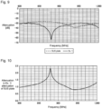
- the attenuation of radio waves by the radio wave absorber prepared in Ex. 1 was measured as follows. As shown in Fig. 8 , radio waves were made to enter the first principal surface 11 of the radio wave absorber 1 from a transmitting antenna 21 at an angle of incidence ⁇ i of 30°. The radio waves reflected at an angle of incidence ⁇ i of 30° were received by a receiving antenna 22. The transmitting antenna 21 and the receiving antenna 22 were disposed symmetrical to the normal to the first principal surface 11 of the radio wave absorber 1 at a position 1000 nm apart from the first principal surface 11. The radio wave absorber 1 was disposed so that the first principal surface 11 stood vertically. The attenuation was obtained as the attenuation of the intensity of received radio waves to the intensity of transmitted radio waves. The frequency of radio waves was from 800 MHz to 1000 MHz. Measurement of the attenuation was conducted in an electromagnetic anechoic chamber, so as to reduce influence of unnecessary radio waves emitted from ones other than the transmitting antenna 21.
- Fig. 9 results of measurement of the attenuation of radio waves by the radio wave absorber prepared in Ex. 1 are shown in Fig. 9 .
- Fig. 9 results of measurement of the attenuation of radio waves by a stainless steel plate (SUS plate) which is a perfect magnetic conductor are also shown.
- SUS plate stainless steel plate
- the attenuation by the SUS plate is negative values due to influence of diffraction and leakage of radio waves.
- the ratio of the attenuation of radio waves by the radio wave absorber prepared in Ex. 1 to the attenuation of radio waves by a SUS plate is shown in Fig. 10 .
- the radio wave absorber prepared in Ex. 1 had large absorption at a frequency in the vicinity of 880 MHz.
- the distance between the conductive layer and the radio wave reflective layer can be made smaller than ⁇ /4, such being preferred in view of weight saving.
- a 8-layered radio wave absorber having a first dielectric layer, a conductive layer, an adhesive layer, a second dielectric layer, an adhesive layer, a radio wave reflective layer, an adhesive layer and a third dielectric layer in this order, shown in Table 10, was prepared.
- the first dielectric layer and the third dielectric layer were soda lime glass having a thickness of 2.75 mm.
- the second dielectric layer was a PC (polycarbonate) substrate having a thickness of 3.0 mm.
- the conductive layer was directly formed on one surface of the first dielectric layer.
- the conductive layer was a laminated film containing silver oxide having a surface resistance of 1.8 ⁇ /sq.
- laser processing was employed.
- L1 was 40 mm
- L2 was 28 mm
- G1 and G2 were 100 ⁇ m.
- As the radio wave reflective layer a metal mesh (surface resistance: 0.01 ⁇ /sq.) woven with stainless steel fibers having a line width of 30 ⁇ m was used.
- a COP film having a relative dielectric constant of 2.33 and a thickness of 380 ⁇ m was used as the adhesive layer. Bonding using the COP film was conducted at a temperature of 130°C with a pressure applied of 1 MPa for a pressurizing time of 90 minutes.
- the radio wave absorber had a 300 mm square first principal surface and had a total thickness of 9.7 mm and a transmittance of 64%.
- the attenuation of radio waves by the radio wave absorber prepared in Ex. 2 was measured in the same manner as the attenuation of radio waves by the radio wave absorber prepared in Ex. 1.
- the measurement results are shown in Fig. 11 .
- results of measurement of the attenuation of radio waves by a SUS plate which is a perfect magnetic conductor are also shown.
- the attenuation by the SUS plate is negative values due to influence of diffraction and leakage of radio waves.
- the ratio of the attenuation of radio waves by the radio wave absorber prepared in Ex. 2 to the attenuation of radio waves by a SUS plate is shown in Fig. 12 . As evident from Figs.
- the radio wave absorber prepared in Ex. 2 had large absorption at a frequency in the vicinity of 924 MHz. Further, the distance between the conductive layer and the radio wave reflective layer can be made smaller than ⁇ /4, such being preferred in view of weight saving.
- radio wave absorber according to the present disclosure has been described above. However, it should be understood that the present invention is by no means restricted to the above specific embodiments. Various changes, modification, replacement, addition, deletion and combination are possible within the scope of Claims. They of course belong to the technical range of the present disclosure.
- the frequency of radio waves absorbed by the radio wave absorber 1 is not limited to 913 MHz for RFID (Radio Frequency IDentification).
- the frequency of radio waves absorbed by the radio wave absorber 1 may, for example, be from 0.5 GHz to 2 GHz, preferably from 0.8 GHz to 1.2 GHz.
- the frequency of radio waves from a mobile phone is 1 GHz.
Landscapes
- Engineering & Computer Science (AREA)
- Microelectronics & Electronic Packaging (AREA)
- Shielding Devices Or Components To Electric Or Magnetic Fields (AREA)
- Laminated Bodies (AREA)
Applications Claiming Priority (2)
| Application Number | Priority Date | Filing Date | Title |
|---|---|---|---|
| JP2020140958 | 2020-08-24 | ||
| PCT/JP2021/030388 WO2022044958A1 (ja) | 2020-08-24 | 2021-08-19 | 電波吸収体 |
Publications (2)
| Publication Number | Publication Date |
|---|---|
| EP4202141A1 true EP4202141A1 (de) | 2023-06-28 |
| EP4202141A4 EP4202141A4 (de) | 2024-08-21 |
Family
ID=80355069
Family Applications (1)
| Application Number | Title | Priority Date | Filing Date |
|---|---|---|---|
| EP21861386.7A Pending EP4202141A4 (de) | 2020-08-24 | 2021-08-19 | Funkwellenabsorber |
Country Status (4)
| Country | Link |
|---|---|
| EP (1) | EP4202141A4 (de) |
| JP (1) | JP7622746B2 (de) |
| CN (1) | CN115917096A (de) |
| WO (1) | WO2022044958A1 (de) |
Families Citing this family (6)
| Publication number | Priority date | Publication date | Assignee | Title |
|---|---|---|---|---|
| CN115425428A (zh) * | 2022-08-16 | 2022-12-02 | 苏州大学 | 一种基于超表面结构的超宽带光学透明微波吸收器件 |
| JP7803331B2 (ja) * | 2022-11-25 | 2026-01-21 | 株式会社デンソー | 電波吸収装置 |
| CN120359667A (zh) * | 2022-11-25 | 2025-07-22 | 株式会社电装 | 电波吸收装置 |
| JP7754151B2 (ja) * | 2022-11-25 | 2025-10-15 | 株式会社デンソー | 電波吸収装置 |
| WO2025023138A1 (ja) * | 2023-07-26 | 2025-01-30 | Agc株式会社 | 電波吸収体 |
| JP2025127972A (ja) * | 2024-02-21 | 2025-09-02 | 国立大学法人東京科学大学 | 電波吸収体 |
Family Cites Families (12)
| Publication number | Priority date | Publication date | Assignee | Title |
|---|---|---|---|---|
| JP3243789B2 (ja) | 1997-03-31 | 2002-01-07 | 日本板硝子株式会社 | 電波吸収性パネル |
| JP4177143B2 (ja) * | 2003-03-14 | 2008-11-05 | 三井化学株式会社 | 電波吸収体 |
| JP4435659B2 (ja) | 2004-09-17 | 2010-03-24 | 三菱電線工業株式会社 | 電波吸収体 |
| JP2009076802A (ja) * | 2007-09-25 | 2009-04-09 | Mitsubishi Cable Ind Ltd | 電波吸収体 |
| JP5162424B2 (ja) * | 2007-12-17 | 2013-03-13 | 藤森工業株式会社 | 電磁波吸収体 |
| JP5222634B2 (ja) * | 2008-06-23 | 2013-06-26 | 藤森工業株式会社 | 周波数選択型の電磁波シールド材を用いた電磁波吸収体 |
| JP2010010612A (ja) * | 2008-06-30 | 2010-01-14 | Asahi Glass Co Ltd | 電磁波吸収体及び電磁波吸収体の製造方法 |
| JP2011091090A (ja) * | 2009-10-20 | 2011-05-06 | Hitachi Chem Co Ltd | 電磁波シールド性透明積層体 |
| JP5689609B2 (ja) * | 2010-03-24 | 2015-03-25 | 三菱製紙株式会社 | 光透過型電波吸収体 |
| JP5831921B2 (ja) * | 2011-03-30 | 2015-12-09 | 日東電工株式会社 | 電磁波吸収体及び電磁波吸収体の製造方法 |
| CN111557129A (zh) * | 2017-12-28 | 2020-08-18 | 日东电工株式会社 | 电磁波吸收体、带有电磁波吸收体的物品、及电磁波吸收体的制造方法 |
| KR102718405B1 (ko) | 2019-02-27 | 2024-10-16 | 에이치알에스코리아 주식회사 | 플러그 커넥터 |
-
2021
- 2021-08-19 EP EP21861386.7A patent/EP4202141A4/de active Pending
- 2021-08-19 WO PCT/JP2021/030388 patent/WO2022044958A1/ja not_active Ceased
- 2021-08-19 CN CN202180051072.7A patent/CN115917096A/zh active Pending
- 2021-08-19 JP JP2022544517A patent/JP7622746B2/ja active Active
Also Published As
| Publication number | Publication date |
|---|---|
| EP4202141A4 (de) | 2024-08-21 |
| CN115917096A (zh) | 2023-04-04 |
| WO2022044958A1 (ja) | 2022-03-03 |
| JPWO2022044958A1 (de) | 2022-03-03 |
| JP7622746B2 (ja) | 2025-01-28 |
Similar Documents
| Publication | Publication Date | Title |
|---|---|---|
| EP4202141A1 (de) | Funkwellenabsorber | |
| JP3243789B2 (ja) | 電波吸収性パネル | |
| JP4176019B2 (ja) | 周波数選択表面を有する電磁エネルギー減衰被覆付き基板 | |
| US8658289B2 (en) | Electromagnetic radiation shielding device | |
| US20130114133A1 (en) | Thin films for energy efficient transparent electromagnetic shields | |
| US20070042819A1 (en) | Wireless network shielding system and method | |
| EP3309343B1 (de) | Verglasungsanordnung | |
| JP2003069282A (ja) | 特定電磁波透過板 | |
| EP4244932B1 (de) | Antennenanordnung | |
| KR102832160B1 (ko) | 전자파 투과 필름 및 윈도우 구조체 | |
| EP4115042B1 (de) | Verglasungseinheit | |
| EP4511913B1 (de) | Kommunikationsvorrichtung und zugehöriges verfahren | |
| JP7613469B2 (ja) | 周波数選択表面装荷部材および車両用窓部材 | |
| JP7683608B2 (ja) | 周波数選択表面装荷部材 | |
| US12607884B2 (en) | Transparent electromagnetic transmission structures for window applications | |
| JP2002076671A (ja) | 電磁波吸収体及び電磁波吸収方法 | |
| EP4266486B1 (de) | Verfahren zur herstellung eines durchsichtigen offenen behälters | |
| KR20250082693A (ko) | 전자파 투과 필름 및 윈도우 구조체 | |
| KR20240168049A (ko) | 도전성 패턴 및 전자파 투과 필름 | |
| KR100524637B1 (ko) | 라디오 파 흡수 판넬 | |
| JP2024094599A (ja) | 収納箱及び物品識別装置 |
Legal Events
| Date | Code | Title | Description |
|---|---|---|---|
| STAA | Information on the status of an ep patent application or granted ep patent |
Free format text: STATUS: THE INTERNATIONAL PUBLICATION HAS BEEN MADE |
|
| PUAI | Public reference made under article 153(3) epc to a published international application that has entered the european phase |
Free format text: ORIGINAL CODE: 0009012 |
|
| STAA | Information on the status of an ep patent application or granted ep patent |
Free format text: STATUS: REQUEST FOR EXAMINATION WAS MADE |
|
| 17P | Request for examination filed |
Effective date: 20230216 |
|
| AK | Designated contracting states |
Kind code of ref document: A1 Designated state(s): AL AT BE BG CH CY CZ DE DK EE ES FI FR GB GR HR HU IE IS IT LI LT LU LV MC MK MT NL NO PL PT RO RS SE SI SK SM TR |
|
| DAV | Request for validation of the european patent (deleted) | ||
| DAX | Request for extension of the european patent (deleted) | ||
| RAP3 | Party data changed (applicant data changed or rights of an application transferred) |
Owner name: AGC INC. |
|
| RIN1 | Information on inventor provided before grant (corrected) |
Inventor name: TANAKA, TSUYOSHI Inventor name: NOGAMI, AKIYO Inventor name: KAWAKAMI, REMI |
|
| REG | Reference to a national code |
Ref country code: DE Ref legal event code: R079 Free format text: PREVIOUS MAIN CLASS: E04B0001920000 Ipc: H01Q0017000000 |
|
| TPAC | Observations filed by third parties |
Free format text: ORIGINAL CODE: EPIDOSNTIPA |
|
| A4 | Supplementary search report drawn up and despatched |
Effective date: 20240719 |
|
| RIC1 | Information provided on ipc code assigned before grant |
Ipc: B32B 27/36 20060101ALN20240716BHEP Ipc: B32B 17/10 20060101ALI20240716BHEP Ipc: H05K 9/00 20060101ALI20240716BHEP Ipc: E04B 1/92 20060101ALI20240716BHEP Ipc: H01Q 17/00 20060101AFI20240716BHEP |
|
| STAA | Information on the status of an ep patent application or granted ep patent |
Free format text: STATUS: EXAMINATION IS IN PROGRESS |