EP4210055A1 - Multiplicateur de matrice vectorielle basé sur la redistribution des charges - Google Patents
Multiplicateur de matrice vectorielle basé sur la redistribution des charges Download PDFInfo
- Publication number
- EP4210055A1 EP4210055A1 EP22150589.4A EP22150589A EP4210055A1 EP 4210055 A1 EP4210055 A1 EP 4210055A1 EP 22150589 A EP22150589 A EP 22150589A EP 4210055 A1 EP4210055 A1 EP 4210055A1
- Authority
- EP
- European Patent Office
- Prior art keywords
- matrix
- input
- vector
- component
- charge storage
- Prior art date
- Legal status (The legal status is an assumption and is not a legal conclusion. Google has not performed a legal analysis and makes no representation as to the accuracy of the status listed.)
- Pending
Links
Images


Classifications
-
- G—PHYSICS
- G11—INFORMATION STORAGE
- G11C—STATIC STORES
- G11C7/00—Arrangements for writing information into, or reading information out from, a digital store
- G11C7/10—Input/output [I/O] data interface arrangements, e.g. I/O data control circuits, I/O data buffers
- G11C7/1006—Data managing, e.g. manipulating data before writing or reading out, data bus switches or control circuits therefor
-
- G—PHYSICS
- G06—COMPUTING OR CALCULATING; COUNTING
- G06N—COMPUTING ARRANGEMENTS BASED ON SPECIFIC COMPUTATIONAL MODELS
- G06N3/00—Computing arrangements based on biological models
- G06N3/02—Neural networks
- G06N3/06—Physical realisation, i.e. hardware implementation of neural networks, neurons or parts of neurons
- G06N3/063—Physical realisation, i.e. hardware implementation of neural networks, neurons or parts of neurons using electronic means
- G06N3/065—Analogue means
Definitions
- the present invention is directed to a programmable in-memory computing device for performing multiplication of an input vector with an input matrix. It is also directed to a method for performing multiplication of an input vector an input matrix having input matrix.
- Matrix operations play an important role in numerous technical applications such as image processing, signal processing, cryptography, and significantly increasingly in the field of artificial intelligence (Al). For example, matrix operations play a central role in artificial neural networks.
- a matrix is an array or table of numbers or expressions arranged in rows and columns. Matrix operations involve multiplying individual factors and adding up (accumulating) whole column products to produce a result.
- Known solutions to implementing matrix operations in technical systems make use of an algorithmic approach using central processing units (CPUs), graphics processing units (GPUs), digital signal processors (DSPs).
- CPUs central processing units
- GPUs graphics processing units
- DSPs digital signal processors
- FPGAs field programmable arrays
- ASIC application specific integrated circuit
- Another disadvantage is a high amount of data transport between memory and the arithmetic unit.
- Resistive random access memory (RRAM) based approaches for the execution of matrix operations are currently a subject of intensive research, e.g. in the realization of neural networks.
- RRAM Resistive random access memory
- I U/R.
- a programmable in-memory computing device for performing multiplication of an input vector of input vector values with an input matrix having input matrix columns of input matrix values.
- the device has a storage component arrangement, hereinafter storage component matrix that comprises
- Each matrix memory component of the storage component matrix comprises
- the matrix memory components of a given matrix component column are each followed by a component product accumulation switch for controlling an output of the charge amount from the respective matrix memory component, and are arranged in a parallel connection with each other and commonly connected in a series connection with a respective column summation charge storage component that is configured to accumulate the respective charge amounts output from the charge storage components so as to generate a column summation output voltage that is indicative of a sum of the component products.
- the mathematical operation of vector-matrix multiplication is implemented in the form of a "natural processing" scheme using the fundamental physical laws governing the charging of capacitors.
- the programmable in-memory computing device of the present invention combines several advantages. It can be implemented in a monolithic integrated circuit fabricated using in any CMOS or BiCMOS technology using the MOS devices that are available in these technologies, such as switches, but also MOS capacitors or (where available) standard MIM or interdigital capacitors as the charge storage components and without requiring additional technology modules. Especially since MOS capacitances can be fabricated in very small size and high area density the in-memory computing device can achieve a particularly good utilization of chip area.
- the in-memory computing device of the present invention is based on a completely different approach for implementation of the multiplication operation.
- RRAM is based on tuneable resistive elements and thus exploits the proportionality of an output voltage to an input current via the programmable ohmic resistance using Ohm's law.
- the solution of the invention is based on the proportionality of an output charge to an input voltage via the capacitance of a tuneable capacitor. Only low charge amounts are required to charge a tuneable capacitor to represent the product of an input vector value and an input matrix value. This allows using particularly small capacitors requiring only small chip area.
- the in-memory computing device of the present invention allows achieving a particularly high resolution of the determined product value, which is higher than that of known RRAM-based devices.
- the device suitably further comprises a column read device for determining a set of column summation output voltages of the column summation charge storage components and for providing a matrix product output signal indicative of the set of the column summation output voltages.
- further embodiments preferably comprise, for each matrix memory component column, a column reset switch, which is connected in parallel to its column summation charge storage component to discharge the summation charge storage component via its connection to the reference potential in its closed state.
- each matrix memory component of one embodiment comprises a respective component reset switch, which is connected in parallel to its charge storage component to discharge the charge storage component via its connection to the reference potential in its closed state.
- the matrix switch phase controller is preferably configured to additionally control discharging of the charge storage components of the matrix memory component in the reset state.
- Different alternative embodiments of the vector input device can be used to provide the input vector values to the matrix memory component. Some embodiments are based on providing an analog input. Other embodiments, which are currently preferred, are based on a digital input. The vector input device of these other embodiments is thus configured to provide to each matrix memory component a digital voltage signal indicative of the respective input vector value.
- each matrix memory component has a digital-to-analog converter, hereinafter V-DAC, which is configured to receive the respective digital voltage signal and provide the respective input vector signal in the form of an analog voltage signal.
- V-DAC digital-to-analog converter
- the matrix switch phase controller is configured to control switching states, i.e., an open or closed state, of the vector input switches of the individual matrix memory components in parallel.
- the digital-to-analog conversion of the digital voltage signals is thus performed in the matrix memory components, suitably between the vector input device and the charge storage component of the given matrix memory component. This allows providing the respective digital voltage signals to the matrix memory components at the same time, i.e. in parallel.
- the vector input device comprises one V-DAC for each column of matrix memory components and is configured to provide to the V-DACs the input vector signals for the respective column as a time sequence.
- the matrix switch phase controller of this embodiment is configured to control switching states of the vector input switches of the individual matrix memory components in correspondence with the time sequence. In comparison with the previous alternative, this embodiment saves chip area by requiring less V-DACs.
- Another group of embodiments provides different solutions for charging the charge storage component with a charge that represents the product of the input vector value and the input matrix value.
- the following embodiments can be combined to form further embodiments.
- the voltage amount of the input vector signal is set in accordance with the respective input vector value during a fixed time span of charging the charge storage component.
- the matrix switch phase controller of this embodiment is configured to control the vector input switch of each matrix memory component to allow the charging of the charge storage component of the respective matrix memory component for a common fixed amount of time.
- the vector input device is configured to provide the vector input signal in the form of an analog voltage signal having a voltage amount uniquely corresponding to the respective input vector value.
- the time span of charging the charge storage component is set in accordance with the respective input vector value, which is provided using a fixed voltage amount.
- the matrix switch phase controller is configured to control the vector input switch of each matrix memory component in the vector load state to allow the charging of the charge storage component of the matrix memory component for a an amount of time that uniquely corresponds to the input vector value.
- the vector input device is configured to provide the vector input signal in the form of an analog voltage signal having a fixed voltage amount.
- a tuneable resistor provided in each matrix memory component is set to a resistance value in accordance with a given input vector value, while a time of charging and a voltage amount applied during the time of charging the tuneable charge storage component are kept constant.
- each matrix memory component comprises between its vector input switch and its charge storage component a resistive element that is tuneable to assume a resistance value uniquely corresponding to a given input vector value.
- the matrix switch phase controller of this embodiment is configured to control the vector input switch of each matrix memory component in the vector load state to allow the charging of the charge storage component of the matrix memory component with the for a common fixed amount of time, and to tune the resistive element to assume a resistance value uniquely corresponding to the current input vector value.
- the vector input device is configured to provide the vector input signal in the form of an analog voltage signal having a fixed voltage amount.
- the charge amount that is transported to the charge storage component of the matrix memory component during a fixed amount of time and under a given applied voltage amount can be varied. This in turn determines the input vector value as one factor of the product of an input vector value and an input matrix value that is computed using the respective matrix memory component.
- the input matrix value is determined by the tuneable capacitance of the charge storage component.
- the tuneable charge storage component is implemented in different embodiments in different ways.
- the tuneable charge storage component is a semiconductor component, and in particular implemented by a p-n junction or an MIS structure of the semiconductor component.
- the semiconductor component is for instance a diode, a varactor or varicap diode, or a bipolar transistor.
- the semiconductor component is for instance a MIS capacitor, such as the well-known gate layer/insulator layer/semiconductor layer structure of a MOS transistor or MOS varactor. All these semiconductor components can be fabricated using a known MOS technology such as a CMOS or BiCMOS technology.
- the thickness of a depletion layer of a reverse-biased pn junction or MOS layer structure varies with the DC voltage applied and provides for a tuneable capacitance.
- the tuneable charge storage component is a C-DAC which can be binary weighted having a plurality of capacitors arranged in parallel, each capacitor corresponding in capacitance value to a power of 2.
- the matrix input signal is preferably implemented as a digital binary signal. The individual bit values of this matrix input signal control activation or deactivation of the capacitances of the tuneable charge storage component in correspondence with the respective input matrix value.
- Other types of C-DACs in particular a C-DAC that is not binary weighted can be used as well, with corresponding adaptation of the matrix input signal.
- a CDAC can consist of several fixed capacitors (MIM or interdigital), which are switched via FET transmission gates.
- a further aspect of the present invention is formed by a method for performing multiplication of an input vector of input vector values with an input matrix having input matrix columns of input matrix values.
- the method comprises:
- VMM vector-matrix multiplication
- the values a to f can be any number or mathematical expression.
- the values are represented by electrical signals, as will be described in more detail below.
- the present specification refers to the vector values as input vector values, and to the matrix values as input matrix values.
- VMM is a frequently-used operation in computing, real-time signal processing, and machine learning.
- In-memory computing devices have been developed to accelerate computing operations such as VMM, in particular by avoiding a transport of data between the processor memory (cache) and a storage system, as required in implementations of the popular von Neumann computer architecture.
- in-memory computing devices suitably have a matrix structure of matrix memory components.
- the matrix memory component forms the elementary building block or memory cell, which is replicated in desired numbers in an in-memory computing device.
- the individual matrix memory components are arranged and connected to represent matrix component rows and matrix component columns of the storage component matrix.
- in-memory computing can be performed in the digital or analog domain
- present specification is directed to an in-memory computing concept that works in the analog domain.
- the analog signal processing performed by the in-memory computing device disclosed in the present specification is advantageous in comparison with digital implementations in particular in terms of required chip area, speed (low number of required clock cycles) and power consumption.
- the computing operation performed by the individual matrix memory components is a multiplication of analog input signals that represent input vector values and input matrix values. Furthermore, an addition or accumulation of determined products is performed, in correspondence with the mathematical rule for performing VMM.
- resistive random access memory (RRAM) based approaches are known for the execution of such matrix operations.
- the present invention employs a charge-redistribution approach. This approach involves an input-dependent charging of a tuneable capacitance for implementing the individual multiplication of an input vector value and an input matrix value in a given matrix memory component, and a subsequent accumulation of the charges from the different matrix memory components of a given matrix column in a respective column summation charge storage component.
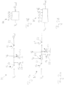
- Figs. 1a shows a simplified circuit diagram of an embodiment of a matrix memory component M for use in a programmable in-memory computing device for performing multiplication of an input vector of input vector values with an input matrix having input matrix columns of input matrix values.
- Fig. 1b is a schematic block representation of this matrix memory component.
- the matrix memory component M receives an analog voltage signal V a from a vector input device (not shown).
- This analog input vector signal uniquely corresponds to an input vector value a of an input vector.
- the present description of Fig. 1a and 1b is based on the use of an input vector signal in the form of an analog electrical signal that has a voltage amount which corresponds to the input vector value a.
- Alternative implementations of the input vector signal will be discussed below.
- the input vector signal V a is fed to a tuneable charge storage component C1 via a vector input switch S1.
- the tuneable charge storage component C1 is connected between a first potential corresponding to a input vector signal V a when the vector input switch is closed, and a reference potential such as a mass or ground potential or any other potential used as a reference.
- the vector input switch S1 is controlled by providing a switching signal ⁇ 1 that assumes either a closed state or an open state.
- the charge Q ad stored on the tuneable charge storage component C1 is achieved to be uniquely correspondent with the product of the tuned capacitance value C d corresponding to a matrix input value d and of the amount of the input vector signal V a that corresponds to the input vector value a.
- the matrix input value d to a control signal determining the capacitance value that is in unique correspondence with the matrix input value.
- the control signal can be provided in the form of single signal component or as a vector signal having a plurality signal components. This will be further elucidated in the context of exemplary implementations of the tuneable charge storage component C1 further below.
- the matrix memory component M further has a component product accumulation switch S2 for blocking or allowing an output of the stored charge amount Q ad from the charge storage component to a summation charge storage component (not shown in Fig. 1a ).
- the switching state of the component product accumulation switch S2 is controlled by an accumulation control signal ⁇ 2 .
- the component product accumulation switch S2 is closed in a summation phase after the vector load phase, the charge amount Q ad stored on the tuneable charge storage component C1 can be output to the summation charge storage component.
- the component product accumulation switch S2 is open, no charge transfer from the tuneable charge storage component C1 towards the summation charge storage component is possible.
- the vector input switches S1 of the individual matrix memory components are open to avoid any further charging of their charge storage components C1.
- a storage component reset switch S3 is connected in parallel to the tuneable charge storage component C1.
- the storage component reset switch is connected on the input side of the tuneable capacitor forming the charge storage component C1 between the vector input switch S1 and C1.
- it may alternatively be arranged on the output side between C1 and the component product accumulation switch S2.
- the storage component reset switch is controlled using a storage component reset signal ⁇ 3 .
- the storage component reset switch is closed, the charge storage component C1 of the matrix memory component M is discharged. This is particularly useful in a reset phase after the summation phase in order to avoid any memory effects.
- the provision of the storage component reset switch S3 may be unnecessary, for instance if the used capacitor technology does not exhibit significant memory effects or a low-ohmic vector voltage source or a sufficient long charging time is used.
- the tuneable charge storage component C1 can be implemented in different forms.
- One implementation is a semiconductor component, such as a semiconductor diode or a transistor with a junction between p- and n-conductive semiconductor regions (pn junction).
- the width of a depletion region formed at the pn junction can be controlled by application of a control voltage V d of suitable polarity, i.e., a reverse voltage and of suitable amount across the pn junction. This way, the capacitance associated with the pn junction is tuned.
- This control voltage is employed in accordance with the present invention as a matrix input signal V d that uniquely corresponds to an input matrix value of an input matrix. By varying the matrix input signal, the capacitance of the charge storage component is varied accordingly.
- FEOL capacitor structures are used for implementing the tuneable charge storage component C1.
- diodes or MOS Caps that are available in known CMOS or BiCMOS FEOL technologies can be used to implement the tuneable charge storage component C1.
- individual semiconductor components of this kind may have a capacitance that is too small for a desired application case.
- a parallel connection of a suitable number of individual semiconductor components or pn-junctions can be used to achieve a desired capacitance value.
- the matrix input signal is then applied to all the pn-junctions or MOS Caps in parallel.
- the present invention is not limited to the use of pn junctions or FEOL capacitor structures as a tuneable capacitance.
- BEOL capacitor structures such as MIM capacitors can be used as well.
- the matrix input signal V d in these cases is suitably a digital signal vector, wherein each vector component is associated with one capacitor of the set of capacitors.
- the capacitors preferably have different capacitance values to achieve a higher resolution in the representation of matrix input values.
- a particular embodiment uses a C-DAC as the tuneable charge storage component.
- the C-DAC is preferably a binary C-DAC with capacitance values representing a sequence of different powers of 2.
- the matrix input signal is preferably provided to the tuneable charge storage component in a binary form, i.e. as a bit string, each bit being used to control one of the capacitors of the C-DAC and to thus individually activate or deactivate it depending on the matrix input value.
- Other types of C-DACs may be used, with appropriate adaptations of the matrix input signal.
- Fig. 1b is a simplified block diagram of the matrix memory component of Fig. 1a that shows only the relevant input and outputs explained in the context of Fig. 1a . This representation will be used in later drawings as a simplified graphical representation of the matrix memory component M.
- Figs. 2a and 2b show a simplified circuit diagram of another embodiment of a matrix memory component M' and a schematic block representation of this matrix memory component.
- the matrix memory component M' resembles the matrix memory component M of Fig. 1 in many aspect. The following description therefore focusses on differences between the two embodiments.
- the matrix memory component M' comprises between its vector input switch S1 and its charge storage component C1 a resistive element R1.
- the resistive element R1 is tuneable to assume a resistance value R a uniquely corresponding to an input vector signal V a .
- the resistance value is thus determined from the input vector value.
- the matrix memory component M' receives a fixed input voltage V IN .
- no DAC is required in the present embodiment for converting the input vector value into the analog domain.
- t 0 is a pre-set time span (charging time span) of application of the input voltage V iN in the vector load phase via the closed input vector switch S1
- R a is the resistance of the tuneable resistor set in accordance with the input vector value
- C d is the capacitance of the tuneable charge storage component set in accordance with the input matrix value.
- the charge amount Q ad that is stored on the charge storage component exhibits a nonlinear dependence with a saturation behavior towards larger charging times (depending on the values of R a and C d ).
- the time span t 0 is suitably selected in a design phase, a device initialization phase or a calibration phase so as to allow arriving at a charge amount that exhibits a technically resolvable unique correspondence with the input vector value (i.e., V a ') over a desired range of values of the product of R a and C d .
- One approach to achieve this is a compensation of the described non-linearity of the above charging function by a suitable pre-distortion of the input voltage V IN as a function of time during the charging time span t 0 .
- the pre-distortion is suitably selected so as to achieve a linearly increasing charge as a function of R a and C d .
- Fig. 2b is a simplified block diagram of the matrix memory component of Fig. 2a that shows only the relevant input and outputs explained in the context of Fig. 2a .
- Fig. 3a is a simplified circuit diagram of a matrix component column MC of an embodiment of a storage component matrix of a programmable in-memory computing device.
- Fig. 3b is a timing diagram for vector input switches for controlling provision of the analog input vector signals for charging the respective charge storage components of the matrix component column of Fig. 3a ;
- the matrix component column MC comprises a number n of matrix memory components M1, M2,...Mn of the type described in the context of Figs. 1a and 1b .
- Switch control signals provided to the individual matrix memory components are labelled with the letter ⁇ and two subscript indices: a first index corresponds to that used in Figs 1a and 1b , and the second index is an order number indicating the position of the respective matrix memory component within the matrix column MC.
- the matrix input signals V d11 , V d12 , ..., V d1n provided to the individual matrix memory components are labelled by V d as in Fig. 1 , followed by two subscript indices indicating the position of the respective matrix value within the input matrix.
- the shown matrix component column is assumed to be the first of n columns, which accounts for the second index "1".
- a vector input device VI is arranged on the input side of the matrix component column MC and provides to the matrix memory components of the matrix columns MC input vector signals V a1 , V a2 , ..., V an that uniquely correspond to respective input vector values a 1 , a 2 , ..., a n of an input vector ( a 1 a 2 ... a n ).
- the input vector is in the present embodiment provided to the vector input device VI in digital form.
- the vector input device has n digital-to-analog converters hereinafter V-DACs labelled VDAC1, VDAC2, ...VDACn.
- Each V-DAC converts one received vector input value into an analog input vector signal that uniquely corresponds to the respective received input vector value of the input vector ( a 1 a 2 ... a n ).
- the vector input device VI provides the analog input vector signals V a1 , V a2 , ..., V an also to matrix memory components of other columns of the storage component matrix, which are not shown in Fig. 3a . Also not shown is a matrix input device that provides the matrix input signals to the individual matrix memory components.
- the matrix memory components M1, M2, ..., Mn of the matrix component column MC are connected in parallel on their output side via a column output line CO.
- This set of parallel-connected matrix components is in turn commonly connected in series with a first electrode of a column summation charge storage component C ⁇ , whose second electrode is connected to the reference potential.
- the column summation charge storage component C ⁇ is configured to accumulate the respective charge amounts output from the charge storage components of the matrix memory components M1, M2,...,Mn so as to generate a column summation output voltage V ⁇ .
- the accumulation in the summation phase results in a charge amount on the column summation charge storage component C ⁇ that equals half the total sum of charge amounts that been loaded onto the tuneable charge storage components in the vector load phase.
- the column summation output voltage is indicative of an output vector element formed by the sum of these products.
- the column summation charge storage component C ⁇ can be implemented as a tuneable capacitor in order to provide for a scaling factor or an option to tune a gain in the column summation output voltage V ⁇ .
- the column summation charge storage component C ⁇ is implemented as a capacitance matrix of a downstream analog-to-digital converter or of an SAR ADC (successive approximation registers analog-to-digital converter).
- the column summation output voltage V ⁇ resulting from the charge accumulation in the column summation charge storage component C ⁇ is indicative of a sum of the component products determined in the individual matrix memory components M1, M2,...Mn.
- a column read device determines the set of column summation output voltages V ⁇ of the column summation charge storage components C ⁇ and provides a matrix product output signal indicative of the set of the column summation output voltages.
- a column reset switch S ⁇ which is connected in parallel to the column summation charge storage component C ⁇ for discharging the summation charge storage component via its connection to the reference potential in its closed state.
- Phase Description S1 S2 S3 S ⁇ 1 loading the matrix with input vector values Closed Open Open Open 2 generating column summation output voltages Open Closed Open Open 3 reading column summation output voltages Open Open Open Open 4 reset Open Open Closed Closed
- phase 1 the vector load phase, closing the vector input switches S1 of the individual matrix memory components ensures that the charge storage components are loaded with a charge amount corresponding to the individual product of input matrix value and input vector value.
- the timing diagram shown in Fig. 3b is a schematic representation of the timing of the individual control signals ⁇ 11 to ⁇ 1n which are respectively provided to the switches S1 of the different matrix memory components M1 to Mn during Phase 1. As can be seen, all charge storage components are loaded at the same time (in parallel) for a common charge time span t 0 . This process is performed in parallel in all columns.
- a respective column output voltage is generated in each of the matrix component columns by transferring and accumulating the charges from the different matrix memory components on the column summation charge storage component C ⁇ during Phase 2, the summation phase.
- the component product accumulation switches S2 are closed while the vector input switches S1 are now open.
- the component product accumulation switches S2 are open again, and the respective voltage generated by the individual charged column summation charge storage components C ⁇ in all n matrix component columns is measured to determine output vector values of the output vector.
- the measurement phase all switches S1 to S3 and S ⁇ are thus open.
- Phase 4 is performed two parts: a first part of Phase 4 is used to reset the tuneable charge storage components of the individual matrix memory components via the reset switches S3. In a second part of Phase 4, the column summation charge storage components C ⁇ in all n matrix component columns are reset.
- This variant is further developed in another variant, which overlaps the second part of Phase 4 with Phase 1 of the next vector-matrix multiplication. This way, a time saving of at least one clock cycle can be achieved. This variant can be used in particular, if no significant memory effects occur after each operation even without resetting.
- Fig. 4a is a simplified circuit diagram of a matrix component column of a further embodiment of a storage component matrix of a programmable in-memory computing device.
- Fig. 4b is a timing diagram for vector input switches for controlling provision of the analog input vector signals for charging the respective charge storage components of the matrix column of Fig. 4a ;
- Fig. 4a The embodiment shown in Fig. 4a largely resembles that of Fig. 3a . For that reason, the following description will only turn to differences. Otherwise, reference is made to the description of Fig. 3a .
- Fig. 4a and 3a differ in the structure of the vector input device.
- Fig. 4a only one digital-to-analog converter VDAC is used for loading the matrix component column with the input vector values. This goes along with a modification of the timing of the control of the vector input switches S1, which is performed by a matrix switch phase controller (not shown).
- the timing diagram shown in Fig. 4b is a schematic representation of the timing of the individual control signals ⁇ 11 to ⁇ 1n which are respectively provided to the switches S1 of the different matrix memory components M1 to Mn during Phase 1.
- the individual charge storage components are loaded one after the other (in series), each for a common charge time span to. This serial process is performed in parallel in all columns, so that the storage component matrix is loaded row by row.
- VDACs assume a significant part of chip area and power dissipation the serialization, i.e., time multiplexing of the provision of the vector input values, allows reducing the hardware expenditure to a single V-DAC.
- this V-DAC charges all capacitances of the matrix component column one after the other. This also represents a significant advantage over the RRAM solution mentioned in the beginning of this specification, since the capacitor holds the charge after charging and no current is required or flowing during the entire operation of the V-DAC.
- the present invention is directed to a programmable in-memory computing device and corresponding method for performing multiplication of an input vector with an input matrix.
- a storage component matrix comprises matrix memory components with a charge storage component that is tuneable by a respective matrix input signal to assume a capacitance value uniquely corresponding to an input matrix value.
- a vector input switch controls provision of the analog input vector signal for charging the charge storage component of the matrix memory component to a charge amount representing a mathematical product of the respective input vector value and the respective input matrix value.
- the matrix memory components of a column are arranged in parallel connection with each other and commonly connected in series connection with a column summation charge storage component which accumulates the charge amounts output from the charge storage components to generate a column summation output voltage indicative of a sum of the component products.
Landscapes
- Engineering & Computer Science (AREA)
- Physics & Mathematics (AREA)
- Health & Medical Sciences (AREA)
- Life Sciences & Earth Sciences (AREA)
- Biomedical Technology (AREA)
- Biophysics (AREA)
- Theoretical Computer Science (AREA)
- Evolutionary Computation (AREA)
- Computational Linguistics (AREA)
- Data Mining & Analysis (AREA)
- Artificial Intelligence (AREA)
- General Health & Medical Sciences (AREA)
- Molecular Biology (AREA)
- Computing Systems (AREA)
- General Engineering & Computer Science (AREA)
- General Physics & Mathematics (AREA)
- Mathematical Physics (AREA)
- Software Systems (AREA)
- Neurology (AREA)
- Complex Calculations (AREA)
Priority Applications (1)
| Application Number | Priority Date | Filing Date | Title |
|---|---|---|---|
| EP22150589.4A EP4210055A1 (fr) | 2022-01-07 | 2022-01-07 | Multiplicateur de matrice vectorielle basé sur la redistribution des charges |
Applications Claiming Priority (1)
| Application Number | Priority Date | Filing Date | Title |
|---|---|---|---|
| EP22150589.4A EP4210055A1 (fr) | 2022-01-07 | 2022-01-07 | Multiplicateur de matrice vectorielle basé sur la redistribution des charges |
Publications (1)
| Publication Number | Publication Date |
|---|---|
| EP4210055A1 true EP4210055A1 (fr) | 2023-07-12 |
Family
ID=79283216
Family Applications (1)
| Application Number | Title | Priority Date | Filing Date |
|---|---|---|---|
| EP22150589.4A Pending EP4210055A1 (fr) | 2022-01-07 | 2022-01-07 | Multiplicateur de matrice vectorielle basé sur la redistribution des charges |
Country Status (1)
| Country | Link |
|---|---|
| EP (1) | EP4210055A1 (fr) |
Cited By (3)
| Publication number | Priority date | Publication date | Assignee | Title |
|---|---|---|---|---|
| EP4579437A1 (fr) | 2023-12-28 | 2025-07-02 | IHP GmbH - Innovations for High Performance Microelectronics / Leibniz-Institut für innovative Mikroelektronik | Linéarisation d'un multiplicateur matriciel vectoriel basé sur une redistribution de charge |
| WO2025140848A1 (fr) | 2023-12-28 | 2025-07-03 | Ihp Gmbh - Innovations For High Performance Microelectronics / Leibniz-Institut Für Innovative Mikroelektronik | Linéarisation d'un multiplicateur de matrice vectorielle basé sur une redistribution de charge |
| WO2026069027A1 (fr) * | 2024-09-30 | 2026-04-02 | International Business Machines Corporation | Multiplication vecteur matrice oscillatoire pour calcul analogique en mémoire (aimc) |
Citations (2)
| Publication number | Priority date | Publication date | Assignee | Title |
|---|---|---|---|---|
| US10580473B2 (en) * | 2014-10-28 | 2020-03-03 | Hewlett Packard Enterprise Development Lp | Memcapacitive cross-bar array for determining a dot product |
| US20210397937A1 (en) * | 2020-06-22 | 2021-12-23 | Qualcomm Incorporated | Charge-pump-based current-mode neuron for machine learning |
-
2022
- 2022-01-07 EP EP22150589.4A patent/EP4210055A1/fr active Pending
Patent Citations (2)
| Publication number | Priority date | Publication date | Assignee | Title |
|---|---|---|---|---|
| US10580473B2 (en) * | 2014-10-28 | 2020-03-03 | Hewlett Packard Enterprise Development Lp | Memcapacitive cross-bar array for determining a dot product |
| US20210397937A1 (en) * | 2020-06-22 | 2021-12-23 | Qualcomm Incorporated | Charge-pump-based current-mode neuron for machine learning |
Non-Patent Citations (1)
| Title |
|---|
| AMIRALI AMIRSOLEIMANI ET AL., ADV. INTELL. SYST., vol. 2, 2020, pages 2000115 |
Cited By (3)
| Publication number | Priority date | Publication date | Assignee | Title |
|---|---|---|---|---|
| EP4579437A1 (fr) | 2023-12-28 | 2025-07-02 | IHP GmbH - Innovations for High Performance Microelectronics / Leibniz-Institut für innovative Mikroelektronik | Linéarisation d'un multiplicateur matriciel vectoriel basé sur une redistribution de charge |
| WO2025140848A1 (fr) | 2023-12-28 | 2025-07-03 | Ihp Gmbh - Innovations For High Performance Microelectronics / Leibniz-Institut Für Innovative Mikroelektronik | Linéarisation d'un multiplicateur de matrice vectorielle basé sur une redistribution de charge |
| WO2026069027A1 (fr) * | 2024-09-30 | 2026-04-02 | International Business Machines Corporation | Multiplication vecteur matrice oscillatoire pour calcul analogique en mémoire (aimc) |
Similar Documents
| Publication | Publication Date | Title |
|---|---|---|
| US11436478B2 (en) | Control circuit for multiply accumulate circuit of neural network system | |
| US11842167B2 (en) | Switched capacitor vector-matrix multiplier | |
| US12242949B2 (en) | Compute-in-memory devices, systems and methods of operation thereof | |
| US11948659B2 (en) | Sub-cell, mac array and bit-width reconfigurable mixed-signal in-memory computing module | |
| Hsieh et al. | 7.6 A 70.85-86.27 TOPS/W PVT-insensitive 8b word-wise ACIM with post-processing relaxation | |
| TWI793277B (zh) | 用於混合訊號運算的系統與方法 | |
| CN112148669B (zh) | 脉冲存算一体芯片以及电子设备 | |
| CN112017713B (zh) | 计算器件以及方法 | |
| TW202349884A (zh) | 用於記憶體內運算巨集的共用行之類比數位轉換器 | |
| Gi et al. | A ReRAM-based convolutional neural network accelerator using the analog layer normalization technique | |
| Caselli et al. | Charge sharing and charge injection A/D converters for analog in-memory computing | |
| US11145339B2 (en) | Device and method for computing-in-memory | |
| Kohda et al. | Unassisted true analog neural network training chip | |
| Al Maharmeh et al. | Compute-in-time for deep neural network accelerators: Challenges and prospects | |
| US10594299B1 (en) | Dynamic resistance element analog counter | |
| Jeong et al. | HYTEC: Compact and Energy-Efficient Analog-Digital Hybrid CIM With Transpose Ternary eDRAM | |
| Lin et al. | A reconfigurable in-SRAM computing architecture for DCNN applications | |
| Radhakrishnan et al. | Bridge memristor super-resolution crossbars | |
| Rasul et al. | A 128x128 SRAM macro with embedded matrix-vector multiplication exploiting passive gain via MOS capacitor for machine learning application | |
| Chae et al. | A Multi-Bit In-Memory-Computing SRAM Macro Using Column-Wise Charge Redistribution for DNN Inference in Edge Computing Devices | |
| Mirchandani et al. | CMOS based Ultra-low Power High-Precision Analog Vector Matrix Multiplication Circuit with±0.1% Error for Vision Application | |
| Biyani et al. | SABCIM: Self-Adaptive Biasing Scheme for Accurate and Efficient Analog Compute-in-Memory | |
| Adam et al. | Evaluating an Analog Main Memory Architecture for All-Analog In-Memory Computing Accelerators | |
| WO2022232055A1 (fr) | Multiplication de vecteur de matrice intégrée exploitant un gain passif par le biais d'un condensateur mosfet pour une application d'apprentissage automatique | |
| EP4579437A1 (fr) | Linéarisation d'un multiplicateur matriciel vectoriel basé sur une redistribution de charge |
Legal Events
| Date | Code | Title | Description |
|---|---|---|---|
| PUAI | Public reference made under article 153(3) epc to a published international application that has entered the european phase |
Free format text: ORIGINAL CODE: 0009012 |
|
| STAA | Information on the status of an ep patent application or granted ep patent |
Free format text: STATUS: THE APPLICATION HAS BEEN PUBLISHED |
|
| AK | Designated contracting states |
Kind code of ref document: A1 Designated state(s): AL AT BE BG CH CY CZ DE DK EE ES FI FR GB GR HR HU IE IS IT LI LT LU LV MC MK MT NL NO PL PT RO RS SE SI SK SM TR |
|
| STAA | Information on the status of an ep patent application or granted ep patent |
Free format text: STATUS: REQUEST FOR EXAMINATION WAS MADE |
|
| 17P | Request for examination filed |
Effective date: 20240112 |
|
| RBV | Designated contracting states (corrected) |
Designated state(s): AL AT BE BG CH CY CZ DE DK EE ES FI FR GB GR HR HU IE IS IT LI LT LU LV MC MK MT NL NO PL PT RO RS SE SI SK SM TR |