EP4579437A1 - Linéarisation d'un multiplicateur matriciel vectoriel basé sur une redistribution de charge - Google Patents
Linéarisation d'un multiplicateur matriciel vectoriel basé sur une redistribution de charge Download PDFInfo
- Publication number
- EP4579437A1 EP4579437A1 EP24159030.6A EP24159030A EP4579437A1 EP 4579437 A1 EP4579437 A1 EP 4579437A1 EP 24159030 A EP24159030 A EP 24159030A EP 4579437 A1 EP4579437 A1 EP 4579437A1
- Authority
- EP
- European Patent Office
- Prior art keywords
- matrix
- summation
- vector
- input
- column
- Prior art date
- Legal status (The legal status is an assumption and is not a legal conclusion. Google has not performed a legal analysis and makes no representation as to the accuracy of the status listed.)
- Pending
Links
Images


Classifications
-
- G—PHYSICS
- G06—COMPUTING OR CALCULATING; COUNTING
- G06F—ELECTRIC DIGITAL DATA PROCESSING
- G06F7/00—Methods or arrangements for processing data by operating upon the order or content of the data handled
- G06F7/38—Methods or arrangements for performing computations using exclusively denominational number representation, e.g. using binary, ternary, decimal representation
- G06F7/48—Methods or arrangements for performing computations using exclusively denominational number representation, e.g. using binary, ternary, decimal representation using non-contact-making devices, e.g. tube, solid state device; using unspecified devices
- G06F7/544—Methods or arrangements for performing computations using exclusively denominational number representation, e.g. using binary, ternary, decimal representation using non-contact-making devices, e.g. tube, solid state device; using unspecified devices for evaluating functions by calculation
- G06F7/5443—Sum of products
-
- G—PHYSICS
- G06—COMPUTING OR CALCULATING; COUNTING
- G06F—ELECTRIC DIGITAL DATA PROCESSING
- G06F17/00—Digital computing or data processing equipment or methods, specially adapted for specific functions
- G06F17/10—Complex mathematical operations
- G06F17/16—Matrix or vector computation, e.g. matrix-matrix or matrix-vector multiplication, matrix factorization
-
- G—PHYSICS
- G06—COMPUTING OR CALCULATING; COUNTING
- G06F—ELECTRIC DIGITAL DATA PROCESSING
- G06F2207/00—Indexing scheme relating to methods or arrangements for processing data by operating upon the order or content of the data handled
- G06F2207/38—Indexing scheme relating to groups G06F7/38 - G06F7/575
- G06F2207/48—Indexing scheme relating to groups G06F7/48 - G06F7/575
- G06F2207/4802—Special implementations
- G06F2207/4814—Non-logic devices, e.g. operational amplifiers
Definitions
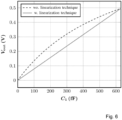
- the present invention is based on the recognition that a parallel connection of the capacitances of the matrix memory components and the summation charge storage component results in a non-linear dependence of the output voltage on the capacitive weight values and thus may lead to inaccurate results of the multiplication.
- a parallel connection of the capacitances of the matrix memory components and the summation charge storage component results in a non-linear dependence of the output voltage on the capacitive weight values and thus may lead to inaccurate results of the multiplication.
- an increase of the capacitive weight values exhibits a non-linear behavior distorting the expected result of the VMM for different sets of weight coefficients.
- the predefined maximal summation capacitance value associated with a given summation charge storage component is the sum of respective maximum capacitance values of the matrix memory components that are connected with the summation charge storage component in the summation phase of operation (cf. below).
- larger values of the upper limit of the tuning range may be chosen if desired in a given application case.
- a second aspect of the present invention is formed by a vector-matrix multiplier which comprises
- the vector-matrix multiplier of the second aspect of the invention shares the advantages described in the context of the accumulator circuit of the first aspect of the present invention.
- the vector-matrix multiplier may comprise a matrix input interface for receiving and providing matrix input signals, which uniquely correspond to respective weight matrix values, to the respective matrix memory components, for setting their tunable capacitances accordingly.
- it additionally comprises a vector input interface for receiving and feeding input vector signals, which uniquely correspond to respective input vector values of the input vector, to the matrix memory components, for charging their set tunable capacitances accordingly.
- the matrix memory components of a given matrix column are each followed by a component product accumulation switch for controlling an output of charge stored in the respective matrix memory component.
- the matrix input interface further comprises, connected to each matrix memory component, a respective analog memory device for receiving and storing the respective matrix input signal in the form of an analog voltage, for output to a tuning control input of the tunable charge storage component of the matrix memory component.
- the vector-matrix multiplier further comprise
- the transfer of the respective charge amounts achieves a voltage balance between the parallel connection of the matrix memory components in the given column and the summation charge storage component of this column.
- the reset phase discharges the matrix memory components (and the summation charge storage component) and thus avoids a detrimental effect of this charge remaining in the matrix memory component at the end of the summation phase on the correct storage of the input vector values to be stored next.
- a method for operating a charge-redistribution based vector-matrix multiplier comprises
- the values of the vector and of the matrix can be any number or mathematical expression.
- the present specification refers to the vector values as input vector values, and to the matrix values as weight matrix values.
- the naming of the input signals to the vector-matrix multiplier is not meant to imply any limitation regarding the meaning of the signals or the spectrum of application cases that can be covered. Names given in the framework of the present specification may have been selected with the purpose of facilitating an intuitive understanding by the reader.
- the values are represented by electrical signals, as will be described in more detail below.
- in-memory computing can be performed in the digital or analog domain
- the present specification is directed to an in-memory computing concept that works in the analog domain.
- the analog signal processing performed by the in-memory computing device disclosed in the present specification is advantageous in comparison with digital implementations in particular in terms of required circuit complexity, speed (low number of required clock cycles) and power consumption.
- the computing operation performed by the individual matrix memory components is a multiplication of analog input signals that represent input vector values and input matrix values.
- a particularly advantageous solution for the accumulation of determined products is disclosed that avoids issues of non-linearity that may be caused by a parallel connection of capacitances , in correspondence with the mathematical rule for performing VMM.
- the memory components are connected between a vector input device and a reference potential such as a ground potential.
- the memory components C ij are formed by tunable charge storage components such as capacitors.
- the memory components C ij are individually tunable in their capacitance value to assume a capacitance value that represents a respective matrix value, for instance a weigh matrix value. They are configured to receive a respective input voltage vector component value of an input voltage vector representing an input vector that is to be multiplied with the matrix.
- the tunable capacitors can thus be used as a synaptic element and their capacitance values represent a respective synaptic weight.
- the values of tunable capacitances C ij represent a synaptic weight matrix, while the voltages Vinj applied to the tunable capacitances C ij of a given column i represent an input vector.
- the tunable charge storage component is a semiconductor component, and in particular implemented by a p-n junction or a MIS structure of the semiconductor component.
- the semiconductor component is for instance a diode, a varactor orvaricap diode, or a bipolar transistor.
- the semiconductor component is for instance a MIS capacitor, such as the well-known gate layer/insulator layer/semiconductor layer structure of a MOS transistor or MOS varactor. All these semiconductor components can be fabricated using a known MOS technology such as a CMOS or BiCMOS technology. The thickness of a depletion layer of a reverse-biased pn junction or MOS layer structure varies with the DC voltage applied and provides for a tunable capacitance.
- the tunable charge storage component is a C-DAC which can be binary weighted having a plurality of capacitors arranged in parallel, each capacitor corresponding in capacitance value to a power of 2.
- the matrix input signal is preferably implemented as a digital binary signal. The individual bit values of this matrix input signal control activation or deactivation of the capacitances of the tunable charge storage component in correspondence with the respective input matrix value.
- SRAM memory cells contain the capacitance values to be configured for the tunable charge storage components. The SRAM memory cells are initially written to after the system has been switched on.
- C-DACs in particular a C-DAC that is not binary weighted can be used as well, with corresponding adaptation of the matrix input signal.
- a C-DAC can consist of several fixed capacitors (MIM or interdigital), which may be similarly switched via FET transmission gates.
- the matrix memory components C ij ,of a given matrix column of the of the vector-matrix multiplier are configured to provide respective charge outputs of an amount corresponding to a product of the respective weight matrix value and the received respective input voltage vector component value of the input voltage vector.
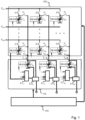
- An output interface of the matrix arrangement 100 has a number output ports O1, O2, ...O M , in correspondence with the number of matrix columns.
- the output ports of the matrix arrangement 100 serve for providing a charge output of the matrix memory components of the given column for accumulation in an accumulator circuit 102 connected with the vector-matrix multiplier 100.
- the output ports may be implemented as nodes in a monolithic electrical circuit in which the matrix arrangement of memory components and the accumulator circuit 102 (to be described below) are co-integrated.
- a linearization controller is configured to generate and provide a column weight sum signal that is indicative of a sum of the current capacitance values of the summation charge storage component and its associated matrix memory components.
- the linearization controller may be implemented as a central control unit, or, as shown in Fig. 1 , in the form of distributed column linearization controllers LC 1 , LC 2 , ..; LC M .
- SRAM cells contain n-bit values in order to activate respective transmission gates for the individual n-bit configurable capacitances.
- the provision of the current capacitance values to the linearization controller may be accomplished by providing the respective content of the SRAMs associated with the summation charge storage component and its associated matrix memory components of a given column as an input to an associated column linearization controller LC 1 , LC 2 , .., or LCnn, respectively
- Fig. 1 shows the column linearization controllers LC 1 , LC 2 , .., or LCnn, as components of the accumulator circuit, this is not mandatory.
- the linearization controller may for instance be implanted as a central unit (not shown) that integrates the functionalities of the different column linearization controllers shown in Fig. 1 .
- the weight values stored in the SRAMs of the matrix memory components may be provided to the column linearization controllers LC' 1 , LC' 2 , .., and LC' M directly from the SRAMS of the associated columns, as shown in Fig.
- an accumulator input interface comprises a number of switchable accumulator input ports I 1 , I 2 , ...I M . each receiving, in a closed switching state, a respective summation charge input corresponding to a sum of charge outputs provided by a set of tunable or adjustable matrix memory components associated with a respective matrix column of the vector-matrix multiplier 100.
- the input ports may be implemented as nodes of an integrated circuit.
- each accumulator input port Connected to each accumulator input port is a respective summation charge storage component C ⁇ i . which in the closed switching state is in a parallel connection with the matrix memory components associated with a respective matrix column, to receive and store the summation charge input provided by the respective matrix column.
Landscapes
- Engineering & Computer Science (AREA)
- Physics & Mathematics (AREA)
- General Physics & Mathematics (AREA)
- Theoretical Computer Science (AREA)
- Pure & Applied Mathematics (AREA)
- Mathematical Analysis (AREA)
- Mathematical Optimization (AREA)
- Mathematical Physics (AREA)
- Computational Mathematics (AREA)
- Computing Systems (AREA)
- Data Mining & Analysis (AREA)
- General Engineering & Computer Science (AREA)
- Algebra (AREA)
- Databases & Information Systems (AREA)
- Software Systems (AREA)
- Complex Calculations (AREA)
Priority Applications (1)
| Application Number | Priority Date | Filing Date | Title |
|---|---|---|---|
| PCT/EP2024/085405 WO2025140848A1 (fr) | 2023-12-28 | 2024-12-10 | Linéarisation d'un multiplicateur de matrice vectorielle basé sur une redistribution de charge |
Applications Claiming Priority (1)
| Application Number | Priority Date | Filing Date | Title |
|---|---|---|---|
| EP23220588 | 2023-12-28 |
Publications (1)
| Publication Number | Publication Date |
|---|---|
| EP4579437A1 true EP4579437A1 (fr) | 2025-07-02 |
Family
ID=89427278
Family Applications (1)
| Application Number | Title | Priority Date | Filing Date |
|---|---|---|---|
| EP24159030.6A Pending EP4579437A1 (fr) | 2023-12-28 | 2024-02-22 | Linéarisation d'un multiplicateur matriciel vectoriel basé sur une redistribution de charge |
Country Status (1)
| Country | Link |
|---|---|
| EP (1) | EP4579437A1 (fr) |
Citations (2)
| Publication number | Priority date | Publication date | Assignee | Title |
|---|---|---|---|---|
| US20130207827A1 (en) * | 2010-08-18 | 2013-08-15 | Analog Devices, Inc. | Charge sharing analog computation circuitry and applications |
| EP4210055A1 (fr) | 2022-01-07 | 2023-07-12 | IHP GmbH - Innovations for High Performance Microelectronics / Leibniz-Institut für innovative Mikroelektronik | Multiplicateur de matrice vectorielle basé sur la redistribution des charges |
-
2024
- 2024-02-22 EP EP24159030.6A patent/EP4579437A1/fr active Pending
Patent Citations (2)
| Publication number | Priority date | Publication date | Assignee | Title |
|---|---|---|---|---|
| US20130207827A1 (en) * | 2010-08-18 | 2013-08-15 | Analog Devices, Inc. | Charge sharing analog computation circuitry and applications |
| EP4210055A1 (fr) | 2022-01-07 | 2023-07-12 | IHP GmbH - Innovations for High Performance Microelectronics / Leibniz-Institut für innovative Mikroelektronik | Multiplicateur de matrice vectorielle basé sur la redistribution des charges |
Similar Documents
| Publication | Publication Date | Title |
|---|---|---|
| US11875249B2 (en) | Counter based resistive processing unit for programmable and reconfigurable artificial-neural-networks | |
| US12242949B2 (en) | Compute-in-memory devices, systems and methods of operation thereof | |
| US20190318239A1 (en) | Resistive processing unit architecture with separate weight update and inference circuitry | |
| US4584568A (en) | Two-step switched-capacitor digital to analog converter | |
| KR20190029406A (ko) | 아날로그 복소 벡터 매트릭스 곱셈을 수행하는 방법 및 시스템 | |
| US20180253643A1 (en) | Analog multiplier-accumulators | |
| GB2583790A (en) | Computing circuitry | |
| US20180225567A1 (en) | Voltage controlled highly linear resistive elements | |
| CN113157034B (zh) | 一种被动稳压电路实现的高线性度神经形态计算电路 | |
| WO2020153989A1 (fr) | Appareil et procédé pour combiner un réseau neuronal analogique avec routage fpga dans un circuit intégré monolithique | |
| EP4210055A1 (fr) | Multiplicateur de matrice vectorielle basé sur la redistribution des charges | |
| CN115913239A (en) | Analog-to-digital conversion circuit, electronic device, and operation method | |
| Caselli et al. | Charge sharing and charge injection A/D converters for analog in-memory computing | |
| US11200948B1 (en) | System for a flexible conductance crossbar | |
| WO2024131396A1 (fr) | Unité tampon de retard et son procédé de fonctionnement, et appareil de calcul et son procédé de fonctionnement | |
| EP4579437A1 (fr) | Linéarisation d'un multiplicateur matriciel vectoriel basé sur une redistribution de charge | |
| Yu et al. | A 4-bit mixed-signal MAC array with swing enhancement and local kernel memory | |
| Sah et al. | Memristor bridge circuit for neural synaptic weighting | |
| WO2025140848A1 (fr) | Linéarisation d'un multiplicateur de matrice vectorielle basé sur une redistribution de charge | |
| KR20210034172A (ko) | Mac 연산 동작을 수행하는 반도체 장치 | |
| US10594299B1 (en) | Dynamic resistance element analog counter | |
| Radhakrishnan et al. | Bridge memristor super-resolution crossbars | |
| JP7675680B2 (ja) | 乗算装置、積和演算装置、行列演算装置およびリザバー装置 | |
| TW202131627A (zh) | 神經放大器、神經網路及感測器裝置 | |
| US20230244919A1 (en) | Reservoir computing apparatus and data processing method |
Legal Events
| Date | Code | Title | Description |
|---|---|---|---|
| PUAI | Public reference made under article 153(3) epc to a published international application that has entered the european phase |
Free format text: ORIGINAL CODE: 0009012 |
|
| STAA | Information on the status of an ep patent application or granted ep patent |
Free format text: STATUS: THE APPLICATION HAS BEEN PUBLISHED |
|
| AK | Designated contracting states |
Kind code of ref document: A1 Designated state(s): AL AT BE BG CH CY CZ DE DK EE ES FI FR GB GR HR HU IE IS IT LI LT LU LV MC ME MK MT NL NO PL PT RO RS SE SI SK SM TR |
|
| STAA | Information on the status of an ep patent application or granted ep patent |
Free format text: STATUS: REQUEST FOR EXAMINATION WAS MADE |
|
| 17P | Request for examination filed |
Effective date: 20260102 |