EP4220686B1 - Procédé de dépôt d'une couche tampon à gradient de contrainte relaxé en silicium-germanium sur une surface d'un substrat - Google Patents
Procédé de dépôt d'une couche tampon à gradient de contrainte relaxé en silicium-germanium sur une surface d'un substrat Download PDFInfo
- Publication number
- EP4220686B1 EP4220686B1 EP22154292.1A EP22154292A EP4220686B1 EP 4220686 B1 EP4220686 B1 EP 4220686B1 EP 22154292 A EP22154292 A EP 22154292A EP 4220686 B1 EP4220686 B1 EP 4220686B1
- Authority
- EP
- European Patent Office
- Prior art keywords
- buffer layer
- stage
- germanium
- less
- substrate
- Prior art date
- Legal status (The legal status is an assumption and is not a legal conclusion. Google has not performed a legal analysis and makes no representation as to the accuracy of the status listed.)
- Active
Links
Images


Classifications
-
- C—CHEMISTRY; METALLURGY
- C23—COATING METALLIC MATERIAL; COATING MATERIAL WITH METALLIC MATERIAL; CHEMICAL SURFACE TREATMENT; DIFFUSION TREATMENT OF METALLIC MATERIAL; COATING BY VACUUM EVAPORATION, BY SPUTTERING, BY ION IMPLANTATION OR BY CHEMICAL VAPOUR DEPOSITION, IN GENERAL; INHIBITING CORROSION OF METALLIC MATERIAL OR INCRUSTATION IN GENERAL
- C23C—COATING METALLIC MATERIAL; COATING MATERIAL WITH METALLIC MATERIAL; SURFACE TREATMENT OF METALLIC MATERIAL BY DIFFUSION INTO THE SURFACE, BY CHEMICAL CONVERSION OR SUBSTITUTION; COATING BY VACUUM EVAPORATION, BY SPUTTERING, BY ION IMPLANTATION OR BY CHEMICAL VAPOUR DEPOSITION, IN GENERAL
- C23C16/00—Chemical coating by decomposition of gaseous compounds, without leaving reaction products of surface material in the coating, i.e. chemical vapour deposition [CVD] processes
- C23C16/06—Chemical coating by decomposition of gaseous compounds, without leaving reaction products of surface material in the coating, i.e. chemical vapour deposition [CVD] processes characterised by the deposition of metallic material
- C23C16/08—Chemical coating by decomposition of gaseous compounds, without leaving reaction products of surface material in the coating, i.e. chemical vapour deposition [CVD] processes characterised by the deposition of metallic material from metal halides
- C23C16/14—Deposition of only one other metal element
-
- H—ELECTRICITY
- H10—SEMICONDUCTOR DEVICES; ELECTRIC SOLID-STATE DEVICES NOT OTHERWISE PROVIDED FOR
- H10P—GENERIC PROCESSES OR APPARATUS FOR THE MANUFACTURE OR TREATMENT OF DEVICES COVERED BY CLASS H10
- H10P14/00—Formation of materials, e.g. in the shape of layers or pillars
- H10P14/20—Formation of materials, e.g. in the shape of layers or pillars of semiconductor materials
- H10P14/32—Formation of materials, e.g. in the shape of layers or pillars of semiconductor materials characterised by intermediate layers between substrates and deposited layers
- H10P14/3202—Materials thereof
- H10P14/3204—Materials thereof being Group IVA semiconducting materials
- H10P14/3211—Silicon, silicon germanium or germanium
-
- H—ELECTRICITY
- H10—SEMICONDUCTOR DEVICES; ELECTRIC SOLID-STATE DEVICES NOT OTHERWISE PROVIDED FOR
- H10P—GENERIC PROCESSES OR APPARATUS FOR THE MANUFACTURE OR TREATMENT OF DEVICES COVERED BY CLASS H10
- H10P14/00—Formation of materials, e.g. in the shape of layers or pillars
- H10P14/20—Formation of materials, e.g. in the shape of layers or pillars of semiconductor materials
- H10P14/24—Formation of materials, e.g. in the shape of layers or pillars of semiconductor materials using chemical vapour deposition [CVD]
-
- H—ELECTRICITY
- H10—SEMICONDUCTOR DEVICES; ELECTRIC SOLID-STATE DEVICES NOT OTHERWISE PROVIDED FOR
- H10P—GENERIC PROCESSES OR APPARATUS FOR THE MANUFACTURE OR TREATMENT OF DEVICES COVERED BY CLASS H10
- H10P14/00—Formation of materials, e.g. in the shape of layers or pillars
- H10P14/20—Formation of materials, e.g. in the shape of layers or pillars of semiconductor materials
- H10P14/29—Formation of materials, e.g. in the shape of layers or pillars of semiconductor materials characterised by the substrates
- H10P14/2901—Materials
- H10P14/2902—Materials being Group IVA materials
- H10P14/2905—Silicon, silicon germanium or germanium
-
- H—ELECTRICITY
- H10—SEMICONDUCTOR DEVICES; ELECTRIC SOLID-STATE DEVICES NOT OTHERWISE PROVIDED FOR
- H10P—GENERIC PROCESSES OR APPARATUS FOR THE MANUFACTURE OR TREATMENT OF DEVICES COVERED BY CLASS H10
- H10P14/00—Formation of materials, e.g. in the shape of layers or pillars
- H10P14/20—Formation of materials, e.g. in the shape of layers or pillars of semiconductor materials
- H10P14/32—Formation of materials, e.g. in the shape of layers or pillars of semiconductor materials characterised by intermediate layers between substrates and deposited layers
- H10P14/3242—Structure
- H10P14/3244—Layer structure
- H10P14/3248—Layer structure consisting of two layers
-
- H—ELECTRICITY
- H10—SEMICONDUCTOR DEVICES; ELECTRIC SOLID-STATE DEVICES NOT OTHERWISE PROVIDED FOR
- H10P—GENERIC PROCESSES OR APPARATUS FOR THE MANUFACTURE OR TREATMENT OF DEVICES COVERED BY CLASS H10
- H10P14/00—Formation of materials, e.g. in the shape of layers or pillars
- H10P14/20—Formation of materials, e.g. in the shape of layers or pillars of semiconductor materials
- H10P14/32—Formation of materials, e.g. in the shape of layers or pillars of semiconductor materials characterised by intermediate layers between substrates and deposited layers
- H10P14/3242—Structure
- H10P14/3244—Layer structure
- H10P14/3254—Graded layers
-
- H—ELECTRICITY
- H10—SEMICONDUCTOR DEVICES; ELECTRIC SOLID-STATE DEVICES NOT OTHERWISE PROVIDED FOR
- H10P—GENERIC PROCESSES OR APPARATUS FOR THE MANUFACTURE OR TREATMENT OF DEVICES COVERED BY CLASS H10
- H10P14/00—Formation of materials, e.g. in the shape of layers or pillars
- H10P14/20—Formation of materials, e.g. in the shape of layers or pillars of semiconductor materials
- H10P14/34—Deposited materials, e.g. layers
- H10P14/3402—Deposited materials, e.g. layers characterised by the chemical composition
- H10P14/3404—Deposited materials, e.g. layers characterised by the chemical composition being Group IVA materials
- H10P14/3411—Silicon, silicon germanium or germanium
-
- C—CHEMISTRY; METALLURGY
- C30—CRYSTAL GROWTH
- C30B—SINGLE-CRYSTAL GROWTH; UNIDIRECTIONAL SOLIDIFICATION OF EUTECTIC MATERIAL OR UNIDIRECTIONAL DEMIXING OF EUTECTOID MATERIAL; REFINING BY ZONE-MELTING OF MATERIAL; PRODUCTION OF A HOMOGENEOUS POLYCRYSTALLINE MATERIAL WITH DEFINED STRUCTURE; SINGLE CRYSTALS OR HOMOGENEOUS POLYCRYSTALLINE MATERIAL WITH DEFINED STRUCTURE; AFTER-TREATMENT OF SINGLE CRYSTALS OR A HOMOGENEOUS POLYCRYSTALLINE MATERIAL WITH DEFINED STRUCTURE; APPARATUS THEREFOR
- C30B29/00—Single crystals or homogeneous polycrystalline material with defined structure characterised by the material or by their shape
- C30B29/02—Elements
- C30B29/06—Silicon
-
- C—CHEMISTRY; METALLURGY
- C30—CRYSTAL GROWTH
- C30B—SINGLE-CRYSTAL GROWTH; UNIDIRECTIONAL SOLIDIFICATION OF EUTECTIC MATERIAL OR UNIDIRECTIONAL DEMIXING OF EUTECTOID MATERIAL; REFINING BY ZONE-MELTING OF MATERIAL; PRODUCTION OF A HOMOGENEOUS POLYCRYSTALLINE MATERIAL WITH DEFINED STRUCTURE; SINGLE CRYSTALS OR HOMOGENEOUS POLYCRYSTALLINE MATERIAL WITH DEFINED STRUCTURE; AFTER-TREATMENT OF SINGLE CRYSTALS OR A HOMOGENEOUS POLYCRYSTALLINE MATERIAL WITH DEFINED STRUCTURE; APPARATUS THEREFOR
- C30B33/00—After-treatment of single crystals or homogeneous polycrystalline material with defined structure
Definitions
- the balance of the two mechanisms (i) and (ii) is of differing importance in different phases of the buffer layer growth.
- In the early stage of the buffer layer growth no dislocations are present within the buffer layer, new loops have to be nucleated to relax the buffer layer, thus (i) is the dominating mechanism.
- (ii) is the dominating mechanism to receive a low TDD.
- the SiGe buffer layer is grown by using a CVD method (chemical vapor deposition) with GeCl 4 and SiH 2 Cl 2 as precursor gases and at a deposition temperature that is not less than 800 °C.
- CVD method chemical vapor deposition
- the growth rate influence on TDD in a first stage of buffer growth (nucleation phase) has been examined in a first set of experiments.
- the sample configuration used in the first set of experiments is depicted in Fig. 1 .
- a graded SiGe buffer layer 2 to a final concentration of 8% Ge was grown on a silicon single crystal wafer 1 ( Fig. 1 ).
- the growth rate was varied from 0.05 ⁇ m/min to 0.8 ⁇ m/min and a grading rate of 4% Ge/ ⁇ m has been used.
- the resulting TDD has been measured after defect selective etching. As shown in Fig. 2 , which displays the TDD over the growth rate GR, the TDD decreases with increasing growth rate to a minimum at 0.46 ⁇ m/min.
- the growth rate influence in second stage of buffer growth has been examined in a second set of experiments.
- the sample configuration used in the second set of experiments is depicted in Fig. 3 .
- a second graded buffer layer 3 was grown to a final concentration of 16% Ge.
- a grading rate of 4% Ge/ ⁇ m has been used.
- the growth rate of the second layer 2 has been varied from 0.05 ⁇ m/min to 0.95 ⁇ m/min. From 0.05 ⁇ m/min to 0.23 ⁇ m/min the TDD increases, at higher growth rates the TDD stays constant. As shown in Fig. 4 , the lowest TDD is realized at lower growth rates.
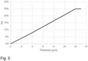
- a full strain relaxed graded buffer layer up to a germanium content of 25% Ge has been deposited on a silicon single crystal wafer in accordance with the claimed invention (example).
- the growth rate was 0.46 ⁇ m / min in accordance with the results of the first set of experiments and in order to generate a low base TDD within the base layer.
- the growth rate was 0.05 ⁇ m / min in accordance with the results of the second set of experiments.
- the overall grading rate was 2.1 % Ge / ⁇ m. As shown in Fig.
Landscapes
- Chemical & Material Sciences (AREA)
- General Chemical & Material Sciences (AREA)
- Chemical Kinetics & Catalysis (AREA)
- Engineering & Computer Science (AREA)
- Materials Engineering (AREA)
- Mechanical Engineering (AREA)
- Metallurgy (AREA)
- Organic Chemistry (AREA)
- Recrystallisation Techniques (AREA)
- Crystals, And After-Treatments Of Crystals (AREA)
- Chemical Vapour Deposition (AREA)
Claims (5)
- Procédé pour le dépôt d'une couche tampon à gradient à contrainte relâchée de silicium germanium sur une surface d'un substrat, la surface étant constituée de silicium et la couche tampon ayant une teneur en germanium qui augmente jusqu'à une teneur finale, le procédé comprenantla conduite de GeCl4 et SiH2Cl2 pendant un premier et un deuxième stade au-dessus de la surface du substrat à une température de dépôt non inférieure à 800 °C,la croissance de la couche tampon avec un taux de gradient qui est inférieur à 10 % de Ge/um, etla croissance de la couche tampon avec une vitesse de croissance qui n'est pas inférieure à 0,1 µm/min pendant le premier stade et qui est inférieure à 0,1 µm/min pendant le deuxième stade.
- Procédé selon la revendication 1, le premier stade ne se terminant pas plus tard que lorsque 1/3 de la teneur totale de germanium a été atteinte.
- Procédé selon la revendication 1 ou la revendication 2, la teneur finale de germanium n'étant pas inférieure à 2 % de Ge et n'étant pas supérieure à 90 % de Ge.
- Procédé selon l'une des revendications 1 à 3, la couche tampon étant déposée par dépôt chimique en phase vapeur.
- Procédé selon l'une des revendications 1 à 4, la couche tampon étant développée sur une plaquette monocristalline de silicium ou sur une plaquette SOI.
Priority Applications (7)
| Application Number | Priority Date | Filing Date | Title |
|---|---|---|---|
| EP22154292.1A EP4220686B1 (fr) | 2022-01-31 | 2022-01-31 | Procédé de dépôt d'une couche tampon à gradient de contrainte relaxé en silicium-germanium sur une surface d'un substrat |
| US18/833,949 US20250101576A1 (en) | 2022-01-31 | 2022-12-14 | Method for depositing a strain relaxed graded buffer layer of silicon germanium on a surface of a substrate |
| KR1020247028941A KR102871173B1 (ko) | 2022-01-31 | 2022-12-14 | 기판의 표면 상에 실리콘 게르마늄의 변형 완화 그레이딩된 버퍼 층을 퇴적시키는 방법 |
| PCT/EP2022/085871 WO2023143804A1 (fr) | 2022-01-31 | 2022-12-14 | Procédé de dépôt d'une couche tampon à gradient et à relaxation de contrainte de silicium-germanium sur une surface d'un substrat |
| CN202280090452.6A CN118633141A (zh) | 2022-01-31 | 2022-12-14 | 用于在衬底的表面上沉积硅锗的应变松弛渐变缓冲层的方法 |
| JP2024543959A JP7693955B2 (ja) | 2022-01-31 | 2022-12-14 | 基板の表面上にシリコンゲルマニウムの歪み緩和傾斜バッファ層を堆積する方法 |
| TW112102157A TWI890021B (zh) | 2022-01-31 | 2023-01-18 | 用於在基板的表面上沉積矽鍺應變鬆弛漸變緩衝層的方法 |
Applications Claiming Priority (1)
| Application Number | Priority Date | Filing Date | Title |
|---|---|---|---|
| EP22154292.1A EP4220686B1 (fr) | 2022-01-31 | 2022-01-31 | Procédé de dépôt d'une couche tampon à gradient de contrainte relaxé en silicium-germanium sur une surface d'un substrat |
Publications (2)
| Publication Number | Publication Date |
|---|---|
| EP4220686A1 EP4220686A1 (fr) | 2023-08-02 |
| EP4220686B1 true EP4220686B1 (fr) | 2024-07-10 |
Family
ID=80119675
Family Applications (1)
| Application Number | Title | Priority Date | Filing Date |
|---|---|---|---|
| EP22154292.1A Active EP4220686B1 (fr) | 2022-01-31 | 2022-01-31 | Procédé de dépôt d'une couche tampon à gradient de contrainte relaxé en silicium-germanium sur une surface d'un substrat |
Country Status (7)
| Country | Link |
|---|---|
| US (1) | US20250101576A1 (fr) |
| EP (1) | EP4220686B1 (fr) |
| JP (1) | JP7693955B2 (fr) |
| KR (1) | KR102871173B1 (fr) |
| CN (1) | CN118633141A (fr) |
| TW (1) | TWI890021B (fr) |
| WO (1) | WO2023143804A1 (fr) |
Family Cites Families (14)
| Publication number | Priority date | Publication date | Assignee | Title |
|---|---|---|---|---|
| DE69827824T3 (de) * | 1997-06-24 | 2009-09-03 | Massachusetts Institute Of Technology, Cambridge | Kontrolle der verspannungsdichte durch verwendung von gradientenschichten und durch planarisierung |
| WO2001022482A1 (fr) * | 1999-09-20 | 2001-03-29 | Amberwave Systems Corporation | Procede de production de couches de silicium-germanium decontractees |
| US7041170B2 (en) * | 1999-09-20 | 2006-05-09 | Amberwave Systems Corporation | Method of producing high quality relaxed silicon germanium layers |
| US6649492B2 (en) * | 2002-02-11 | 2003-11-18 | International Business Machines Corporation | Strained Si based layer made by UHV-CVD, and devices therein |
| AU2003222003A1 (en) * | 2002-03-14 | 2003-09-29 | Amberwave Systems Corporation | Methods for fabricating strained layers on semiconductor substrates |
| US7332417B2 (en) * | 2003-01-27 | 2008-02-19 | Amberwave Systems Corporation | Semiconductor structures with structural homogeneity |
| EP1604395A2 (fr) | 2003-03-13 | 2005-12-14 | ASM America, Inc. | Procedes de depot epitaxial de semiconducteur et structures correspondantes |
| DE102005000826A1 (de) | 2005-01-05 | 2006-07-20 | Siltronic Ag | Halbleiterscheibe mit Silicium-Germanium-Schicht und Verfahren zu deren Herstellung |
| US7902046B2 (en) | 2005-09-19 | 2011-03-08 | The Board Of Trustees Of The Leland Stanford Junior University | Thin buffer layers for SiGe growth on mismatched substrates |
| JP2007194336A (ja) * | 2006-01-18 | 2007-08-02 | Sumco Corp | 半導体ウェーハの製造方法 |
| EP2104135B1 (fr) | 2008-03-20 | 2013-06-12 | Siltronic AG | Plaquette semiconductrice dotée d'une couche hétéroépitaxiale et procédé pour la fabrication de la plaquette |
| US9343303B2 (en) * | 2014-03-20 | 2016-05-17 | Samsung Electronics Co., Ltd. | Methods of forming low-defect strain-relaxed layers on lattice-mismatched substrates and related semiconductor structures and devices |
| US9691860B2 (en) | 2014-05-02 | 2017-06-27 | Samsung Electronics Co., Ltd. | Methods of forming defect-free SRB onto lattice-mismatched substrates and defect-free fins on insulators |
| FR3061803B1 (fr) * | 2017-01-11 | 2019-08-16 | Soitec | Substrat pour capteur d'image de type face avant et procede de fabrication d'un tel substrat |
-
2022
- 2022-01-31 EP EP22154292.1A patent/EP4220686B1/fr active Active
- 2022-12-14 WO PCT/EP2022/085871 patent/WO2023143804A1/fr not_active Ceased
- 2022-12-14 US US18/833,949 patent/US20250101576A1/en active Pending
- 2022-12-14 CN CN202280090452.6A patent/CN118633141A/zh active Pending
- 2022-12-14 KR KR1020247028941A patent/KR102871173B1/ko active Active
- 2022-12-14 JP JP2024543959A patent/JP7693955B2/ja active Active
-
2023
- 2023-01-18 TW TW112102157A patent/TWI890021B/zh active
Also Published As
| Publication number | Publication date |
|---|---|
| TWI890021B (zh) | 2025-07-11 |
| KR102871173B1 (ko) | 2025-10-14 |
| KR20240140956A (ko) | 2024-09-24 |
| WO2023143804A1 (fr) | 2023-08-03 |
| CN118633141A (zh) | 2024-09-10 |
| JP2025503787A (ja) | 2025-02-04 |
| TW202332814A (zh) | 2023-08-16 |
| EP4220686A1 (fr) | 2023-08-02 |
| JP7693955B2 (ja) | 2025-06-17 |
| US20250101576A1 (en) | 2025-03-27 |
Similar Documents
| Publication | Publication Date | Title |
|---|---|---|
| JP4850960B2 (ja) | エピタキシャル炭化珪素単結晶基板の製造方法 | |
| US7666799B2 (en) | Epitaxial growth of relaxed silicon germanium layers | |
| KR101037636B1 (ko) | 헤테로에피텍셜 층을 지닌 반도체 웨이퍼 및 반도체 웨이퍼제조 방법 | |
| EP2016205B1 (fr) | STRUCTURES DE COUCHES TAMPON SEMI-CONDUCTRICES DE SiGe AUX CONTRAINTES RELAXEES | |
| Atzmon et al. | Chemical vapor deposition of heteroepitaxial Si1− x− y Ge x C y films on (100) Si substrates | |
| KR101971597B1 (ko) | 웨이퍼 및 박막 제조 방법 | |
| EP2064729A2 (fr) | Structures semi-conductrices épaisses au nitrure, comprenant des structures de couche intermédiaires, et procédés de fabrication de structures semi-conductrices épaisses au nitrure | |
| WO2001022482A9 (fr) | Procede de production de couches de silicium-germanium decontractees | |
| Kissinger et al. | Stepwise equilibrated graded Ge x Si1− x buffer with very low threading dislocation density on Si (001) | |
| JP2023045163A (ja) | ヘテロエピタキシャルウェーハの製造方法 | |
| EP4220686B1 (fr) | Procédé de dépôt d'une couche tampon à gradient de contrainte relaxé en silicium-germanium sur une surface d'un substrat | |
| AU651568B2 (en) | Method for forming crystalline deposited film | |
| JP4700472B2 (ja) | 基板およびこの上にヘテロエピタキシャル堆積した珪素とゲルマニウムからなる層を有する多層構造体の製造方法 | |
| JP4158607B2 (ja) | 半導体基板の製造方法 | |
| JP7218832B1 (ja) | ヘテロエピタキシャルウェーハの製造方法 | |
| US8115195B2 (en) | Semiconductor wafer with a heteroepitaxial layer and a method for producing the wafer | |
| JP2004349522A (ja) | 半導体基板の製造方法 | |
| WO2023058355A1 (fr) | Procédé pour la formation d'un film hétéroépitaxial | |
| CN121161418A (zh) | 一种高质量碳化硅同质外延片及其制备方法 |
Legal Events
| Date | Code | Title | Description |
|---|---|---|---|
| PUAI | Public reference made under article 153(3) epc to a published international application that has entered the european phase |
Free format text: ORIGINAL CODE: 0009012 |
|
| STAA | Information on the status of an ep patent application or granted ep patent |
Free format text: STATUS: THE APPLICATION HAS BEEN PUBLISHED |
|
| AK | Designated contracting states |
Kind code of ref document: A1 Designated state(s): AL AT BE BG CH CY CZ DE DK EE ES FI FR GB GR HR HU IE IS IT LI LT LU LV MC MK MT NL NO PL PT RO RS SE SI SK SM TR |
|
| STAA | Information on the status of an ep patent application or granted ep patent |
Free format text: STATUS: REQUEST FOR EXAMINATION WAS MADE |
|
| 17P | Request for examination filed |
Effective date: 20230915 |
|
| RBV | Designated contracting states (corrected) |
Designated state(s): AL AT BE BG CH CY CZ DE DK EE ES FI FR GB GR HR HU IE IS IT LI LT LU LV MC MK MT NL NO PL PT RO RS SE SI SK SM TR |
|
| GRAP | Despatch of communication of intention to grant a patent |
Free format text: ORIGINAL CODE: EPIDOSNIGR1 |
|
| STAA | Information on the status of an ep patent application or granted ep patent |
Free format text: STATUS: GRANT OF PATENT IS INTENDED |
|
| RIC1 | Information provided on ipc code assigned before grant |
Ipc: H01L 21/20 20060101AFI20240201BHEP |
|
| INTG | Intention to grant announced |
Effective date: 20240220 |
|
| GRAS | Grant fee paid |
Free format text: ORIGINAL CODE: EPIDOSNIGR3 |
|
| GRAA | (expected) grant |
Free format text: ORIGINAL CODE: 0009210 |
|
| STAA | Information on the status of an ep patent application or granted ep patent |
Free format text: STATUS: THE PATENT HAS BEEN GRANTED |
|
| AK | Designated contracting states |
Kind code of ref document: B1 Designated state(s): AL AT BE BG CH CY CZ DE DK EE ES FI FR GB GR HR HU IE IS IT LI LT LU LV MC MK MT NL NO PL PT RO RS SE SI SK SM TR |
|
| REG | Reference to a national code |
Ref country code: CH Ref legal event code: EP |
|
| REG | Reference to a national code |
Ref country code: DE Ref legal event code: R096 Ref document number: 602022004380 Country of ref document: DE |
|
| REG | Reference to a national code |
Ref country code: LT Ref legal event code: MG9D |
|
| REG | Reference to a national code |
Ref country code: NL Ref legal event code: MP Effective date: 20240710 |
|
| PG25 | Lapsed in a contracting state [announced via postgrant information from national office to epo] |
Ref country code: PT Free format text: LAPSE BECAUSE OF FAILURE TO SUBMIT A TRANSLATION OF THE DESCRIPTION OR TO PAY THE FEE WITHIN THE PRESCRIBED TIME-LIMIT Effective date: 20241111 |
|
| REG | Reference to a national code |
Ref country code: AT Ref legal event code: MK05 Ref document number: 1702814 Country of ref document: AT Kind code of ref document: T Effective date: 20240710 |
|
| PG25 | Lapsed in a contracting state [announced via postgrant information from national office to epo] |
Ref country code: NL Free format text: LAPSE BECAUSE OF FAILURE TO SUBMIT A TRANSLATION OF THE DESCRIPTION OR TO PAY THE FEE WITHIN THE PRESCRIBED TIME-LIMIT Effective date: 20240710 |
|
| PG25 | Lapsed in a contracting state [announced via postgrant information from national office to epo] |
Ref country code: PT Free format text: LAPSE BECAUSE OF FAILURE TO SUBMIT A TRANSLATION OF THE DESCRIPTION OR TO PAY THE FEE WITHIN THE PRESCRIBED TIME-LIMIT Effective date: 20241111 Ref country code: NL Free format text: LAPSE BECAUSE OF FAILURE TO SUBMIT A TRANSLATION OF THE DESCRIPTION OR TO PAY THE FEE WITHIN THE PRESCRIBED TIME-LIMIT Effective date: 20240710 |
|
| PG25 | Lapsed in a contracting state [announced via postgrant information from national office to epo] |
Ref country code: NO Free format text: LAPSE BECAUSE OF FAILURE TO SUBMIT A TRANSLATION OF THE DESCRIPTION OR TO PAY THE FEE WITHIN THE PRESCRIBED TIME-LIMIT Effective date: 20241010 |
|
| PG25 | Lapsed in a contracting state [announced via postgrant information from national office to epo] |
Ref country code: GR Free format text: LAPSE BECAUSE OF FAILURE TO SUBMIT A TRANSLATION OF THE DESCRIPTION OR TO PAY THE FEE WITHIN THE PRESCRIBED TIME-LIMIT Effective date: 20241011 Ref country code: FI Free format text: LAPSE BECAUSE OF FAILURE TO SUBMIT A TRANSLATION OF THE DESCRIPTION OR TO PAY THE FEE WITHIN THE PRESCRIBED TIME-LIMIT Effective date: 20240710 Ref country code: PL Free format text: LAPSE BECAUSE OF FAILURE TO SUBMIT A TRANSLATION OF THE DESCRIPTION OR TO PAY THE FEE WITHIN THE PRESCRIBED TIME-LIMIT Effective date: 20240710 |
|
| PG25 | Lapsed in a contracting state [announced via postgrant information from national office to epo] |
Ref country code: BG Free format text: LAPSE BECAUSE OF FAILURE TO SUBMIT A TRANSLATION OF THE DESCRIPTION OR TO PAY THE FEE WITHIN THE PRESCRIBED TIME-LIMIT Effective date: 20240710 |
|
| PG25 | Lapsed in a contracting state [announced via postgrant information from national office to epo] |
Ref country code: LV Free format text: LAPSE BECAUSE OF FAILURE TO SUBMIT A TRANSLATION OF THE DESCRIPTION OR TO PAY THE FEE WITHIN THE PRESCRIBED TIME-LIMIT Effective date: 20240710 |
|
| PG25 | Lapsed in a contracting state [announced via postgrant information from national office to epo] |
Ref country code: AT Free format text: LAPSE BECAUSE OF FAILURE TO SUBMIT A TRANSLATION OF THE DESCRIPTION OR TO PAY THE FEE WITHIN THE PRESCRIBED TIME-LIMIT Effective date: 20240710 Ref country code: IS Free format text: LAPSE BECAUSE OF FAILURE TO SUBMIT A TRANSLATION OF THE DESCRIPTION OR TO PAY THE FEE WITHIN THE PRESCRIBED TIME-LIMIT Effective date: 20241110 |
|
| PG25 | Lapsed in a contracting state [announced via postgrant information from national office to epo] |
Ref country code: HR Free format text: LAPSE BECAUSE OF FAILURE TO SUBMIT A TRANSLATION OF THE DESCRIPTION OR TO PAY THE FEE WITHIN THE PRESCRIBED TIME-LIMIT Effective date: 20240710 |
|
| PG25 | Lapsed in a contracting state [announced via postgrant information from national office to epo] |
Ref country code: ES Free format text: LAPSE BECAUSE OF FAILURE TO SUBMIT A TRANSLATION OF THE DESCRIPTION OR TO PAY THE FEE WITHIN THE PRESCRIBED TIME-LIMIT Effective date: 20240710 Ref country code: RS Free format text: LAPSE BECAUSE OF FAILURE TO SUBMIT A TRANSLATION OF THE DESCRIPTION OR TO PAY THE FEE WITHIN THE PRESCRIBED TIME-LIMIT Effective date: 20241010 |
|
| PG25 | Lapsed in a contracting state [announced via postgrant information from national office to epo] |
Ref country code: RS Free format text: LAPSE BECAUSE OF FAILURE TO SUBMIT A TRANSLATION OF THE DESCRIPTION OR TO PAY THE FEE WITHIN THE PRESCRIBED TIME-LIMIT Effective date: 20241010 Ref country code: PL Free format text: LAPSE BECAUSE OF FAILURE TO SUBMIT A TRANSLATION OF THE DESCRIPTION OR TO PAY THE FEE WITHIN THE PRESCRIBED TIME-LIMIT Effective date: 20240710 Ref country code: NO Free format text: LAPSE BECAUSE OF FAILURE TO SUBMIT A TRANSLATION OF THE DESCRIPTION OR TO PAY THE FEE WITHIN THE PRESCRIBED TIME-LIMIT Effective date: 20241010 Ref country code: LV Free format text: LAPSE BECAUSE OF FAILURE TO SUBMIT A TRANSLATION OF THE DESCRIPTION OR TO PAY THE FEE WITHIN THE PRESCRIBED TIME-LIMIT Effective date: 20240710 Ref country code: IS Free format text: LAPSE BECAUSE OF FAILURE TO SUBMIT A TRANSLATION OF THE DESCRIPTION OR TO PAY THE FEE WITHIN THE PRESCRIBED TIME-LIMIT Effective date: 20241110 Ref country code: HR Free format text: LAPSE BECAUSE OF FAILURE TO SUBMIT A TRANSLATION OF THE DESCRIPTION OR TO PAY THE FEE WITHIN THE PRESCRIBED TIME-LIMIT Effective date: 20240710 Ref country code: GR Free format text: LAPSE BECAUSE OF FAILURE TO SUBMIT A TRANSLATION OF THE DESCRIPTION OR TO PAY THE FEE WITHIN THE PRESCRIBED TIME-LIMIT Effective date: 20241011 Ref country code: FI Free format text: LAPSE BECAUSE OF FAILURE TO SUBMIT A TRANSLATION OF THE DESCRIPTION OR TO PAY THE FEE WITHIN THE PRESCRIBED TIME-LIMIT Effective date: 20240710 Ref country code: ES Free format text: LAPSE BECAUSE OF FAILURE TO SUBMIT A TRANSLATION OF THE DESCRIPTION OR TO PAY THE FEE WITHIN THE PRESCRIBED TIME-LIMIT Effective date: 20240710 Ref country code: BG Free format text: LAPSE BECAUSE OF FAILURE TO SUBMIT A TRANSLATION OF THE DESCRIPTION OR TO PAY THE FEE WITHIN THE PRESCRIBED TIME-LIMIT Effective date: 20240710 Ref country code: AT Free format text: LAPSE BECAUSE OF FAILURE TO SUBMIT A TRANSLATION OF THE DESCRIPTION OR TO PAY THE FEE WITHIN THE PRESCRIBED TIME-LIMIT Effective date: 20240710 |
|
| REG | Reference to a national code |
Ref country code: DE Ref legal event code: R097 Ref document number: 602022004380 Country of ref document: DE |
|
| PG25 | Lapsed in a contracting state [announced via postgrant information from national office to epo] |
Ref country code: RO Free format text: LAPSE BECAUSE OF FAILURE TO SUBMIT A TRANSLATION OF THE DESCRIPTION OR TO PAY THE FEE WITHIN THE PRESCRIBED TIME-LIMIT Effective date: 20240710 Ref country code: DK Free format text: LAPSE BECAUSE OF FAILURE TO SUBMIT A TRANSLATION OF THE DESCRIPTION OR TO PAY THE FEE WITHIN THE PRESCRIBED TIME-LIMIT Effective date: 20240710 Ref country code: SM Free format text: LAPSE BECAUSE OF FAILURE TO SUBMIT A TRANSLATION OF THE DESCRIPTION OR TO PAY THE FEE WITHIN THE PRESCRIBED TIME-LIMIT Effective date: 20240710 |
|
| PG25 | Lapsed in a contracting state [announced via postgrant information from national office to epo] |
Ref country code: EE Free format text: LAPSE BECAUSE OF FAILURE TO SUBMIT A TRANSLATION OF THE DESCRIPTION OR TO PAY THE FEE WITHIN THE PRESCRIBED TIME-LIMIT Effective date: 20240710 |
|
| PG25 | Lapsed in a contracting state [announced via postgrant information from national office to epo] |
Ref country code: CZ Free format text: LAPSE BECAUSE OF FAILURE TO SUBMIT A TRANSLATION OF THE DESCRIPTION OR TO PAY THE FEE WITHIN THE PRESCRIBED TIME-LIMIT Effective date: 20240710 |
|
| PG25 | Lapsed in a contracting state [announced via postgrant information from national office to epo] |
Ref country code: SK Free format text: LAPSE BECAUSE OF FAILURE TO SUBMIT A TRANSLATION OF THE DESCRIPTION OR TO PAY THE FEE WITHIN THE PRESCRIBED TIME-LIMIT Effective date: 20240710 |
|
| PLBE | No opposition filed within time limit |
Free format text: ORIGINAL CODE: 0009261 |
|
| STAA | Information on the status of an ep patent application or granted ep patent |
Free format text: STATUS: NO OPPOSITION FILED WITHIN TIME LIMIT |
|
| 26N | No opposition filed |
Effective date: 20250411 |
|
| REG | Reference to a national code |
Ref country code: CH Ref legal event code: PL |
|
| PG25 | Lapsed in a contracting state [announced via postgrant information from national office to epo] |
Ref country code: SE Free format text: LAPSE BECAUSE OF FAILURE TO SUBMIT A TRANSLATION OF THE DESCRIPTION OR TO PAY THE FEE WITHIN THE PRESCRIBED TIME-LIMIT Effective date: 20240710 |
|
| PG25 | Lapsed in a contracting state [announced via postgrant information from national office to epo] |
Ref country code: LU Free format text: LAPSE BECAUSE OF NON-PAYMENT OF DUE FEES Effective date: 20250131 Ref country code: MC Free format text: LAPSE BECAUSE OF FAILURE TO SUBMIT A TRANSLATION OF THE DESCRIPTION OR TO PAY THE FEE WITHIN THE PRESCRIBED TIME-LIMIT Effective date: 20240710 |
|
| PG25 | Lapsed in a contracting state [announced via postgrant information from national office to epo] |
Ref country code: BE Free format text: LAPSE BECAUSE OF NON-PAYMENT OF DUE FEES Effective date: 20250131 |
|
| PG25 | Lapsed in a contracting state [announced via postgrant information from national office to epo] |
Ref country code: CH Free format text: LAPSE BECAUSE OF NON-PAYMENT OF DUE FEES Effective date: 20250131 |
|
| REG | Reference to a national code |
Ref country code: BE Ref legal event code: MM Effective date: 20250131 |
|
| REG | Reference to a national code |
Ref country code: DE Ref legal event code: R079 Ref document number: 602022004380 Country of ref document: DE Free format text: PREVIOUS MAIN CLASS: H01L0021200000 Ipc: H10P0014200000 |
|
| PGFP | Annual fee paid to national office [announced via postgrant information from national office to epo] |
Ref country code: IE Payment date: 20260120 Year of fee payment: 5 Ref country code: DE Payment date: 20260127 Year of fee payment: 5 |
|
| PGFP | Annual fee paid to national office [announced via postgrant information from national office to epo] |
Ref country code: IT Payment date: 20260123 Year of fee payment: 5 |
|
| PGFP | Annual fee paid to national office [announced via postgrant information from national office to epo] |
Ref country code: FR Payment date: 20260126 Year of fee payment: 5 |