EP4220699A1 - Herstellungsverfahren für eine halbleiterstruktur - Google Patents
Herstellungsverfahren für eine halbleiterstruktur Download PDFInfo
- Publication number
- EP4220699A1 EP4220699A1 EP21940441.5A EP21940441A EP4220699A1 EP 4220699 A1 EP4220699 A1 EP 4220699A1 EP 21940441 A EP21940441 A EP 21940441A EP 4220699 A1 EP4220699 A1 EP 4220699A1
- Authority
- EP
- European Patent Office
- Prior art keywords
- mask layers
- mask
- layers
- layer
- forming
- Prior art date
- Legal status (The legal status is an assumption and is not a legal conclusion. Google has not performed a legal analysis and makes no representation as to the accuracy of the status listed.)
- Granted
Links
Images






Classifications
-
- H—ELECTRICITY
- H10—SEMICONDUCTOR DEVICES; ELECTRIC SOLID-STATE DEVICES NOT OTHERWISE PROVIDED FOR
- H10P—GENERIC PROCESSES OR APPARATUS FOR THE MANUFACTURE OR TREATMENT OF DEVICES COVERED BY CLASS H10
- H10P50/00—Etching of wafers, substrates or parts of devices
- H10P50/69—Etching of wafers, substrates or parts of devices using masks for semiconductor materials
- H10P50/691—Etching of wafers, substrates or parts of devices using masks for semiconductor materials for Group V materials or Group III-V materials
- H10P50/693—Etching of wafers, substrates or parts of devices using masks for semiconductor materials for Group V materials or Group III-V materials characterised by their size, orientation, disposition, behaviour or shape, in horizontal or vertical plane
- H10P50/695—Etching of wafers, substrates or parts of devices using masks for semiconductor materials for Group V materials or Group III-V materials characterised by their size, orientation, disposition, behaviour or shape, in horizontal or vertical plane characterised by the process involved to create the mask, e.g. lift-off masks or sidewalls or to modify the mask
-
- H—ELECTRICITY
- H10—SEMICONDUCTOR DEVICES; ELECTRIC SOLID-STATE DEVICES NOT OTHERWISE PROVIDED FOR
- H10P—GENERIC PROCESSES OR APPARATUS FOR THE MANUFACTURE OR TREATMENT OF DEVICES COVERED BY CLASS H10
- H10P50/00—Etching of wafers, substrates or parts of devices
- H10P50/69—Etching of wafers, substrates or parts of devices using masks for semiconductor materials
- H10P50/691—Etching of wafers, substrates or parts of devices using masks for semiconductor materials for Group V materials or Group III-V materials
- H10P50/692—Etching of wafers, substrates or parts of devices using masks for semiconductor materials for Group V materials or Group III-V materials characterised by their composition, e.g. multilayer masks or materials
-
- H—ELECTRICITY
- H10—SEMICONDUCTOR DEVICES; ELECTRIC SOLID-STATE DEVICES NOT OTHERWISE PROVIDED FOR
- H10B—ELECTRONIC MEMORY DEVICES
- H10B12/00—Dynamic random access memory [DRAM] devices
- H10B12/30—DRAM devices comprising one-transistor - one-capacitor [1T-1C] memory cells
- H10B12/48—Data lines or contacts therefor
- H10B12/488—Word lines
-
- H—ELECTRICITY
- H10—SEMICONDUCTOR DEVICES; ELECTRIC SOLID-STATE DEVICES NOT OTHERWISE PROVIDED FOR
- H10D—INORGANIC ELECTRIC SEMICONDUCTOR DEVICES
- H10D64/00—Electrodes of devices having potential barriers
- H10D64/01—Manufacture or treatment
- H10D64/031—Manufacture or treatment of data-storage electrodes
-
- H—ELECTRICITY
- H10—SEMICONDUCTOR DEVICES; ELECTRIC SOLID-STATE DEVICES NOT OTHERWISE PROVIDED FOR
- H10W—GENERIC PACKAGES, INTERCONNECTIONS, CONNECTORS OR OTHER CONSTRUCTIONAL DETAILS OF DEVICES COVERED BY CLASS H10
- H10W10/00—Isolation regions in semiconductor bodies between components of integrated devices
- H10W10/01—Manufacture or treatment
- H10W10/011—Manufacture or treatment of isolation regions comprising dielectric materials
- H10W10/014—Manufacture or treatment of isolation regions comprising dielectric materials using trench refilling with dielectric materials, e.g. shallow trench isolations
-
- H—ELECTRICITY
- H10—SEMICONDUCTOR DEVICES; ELECTRIC SOLID-STATE DEVICES NOT OTHERWISE PROVIDED FOR
- H10W—GENERIC PACKAGES, INTERCONNECTIONS, CONNECTORS OR OTHER CONSTRUCTIONAL DETAILS OF DEVICES COVERED BY CLASS H10
- H10W10/00—Isolation regions in semiconductor bodies between components of integrated devices
- H10W10/10—Isolation regions comprising dielectric materials
- H10W10/17—Isolation regions comprising dielectric materials formed using trench refilling with dielectric materials, e.g. shallow trench isolations
Definitions
- the present disclosure relates to, but is not limited to, a method of manufacturing a semiconductor structure.
- DRAM dynamic random access memory
- the DRAM generally includes structures such as a base, a word line and active regions.
- the active regions are generally formed by using a self-aligned double patterning (SADP) technology.
- SADP self-aligned double patterning
- the active regions are prone to tilt or collapse, which may cause structural failure and reduce the yield of a semiconductor structure.
- the embodiments of the present disclosure provide a method of manufacturing a semiconductor structure.
- the method of manufacturing a semiconductor structure includes:
- the second mask layers each span a plurality of the first mask layers.
- the second mask layers can achieve an effect of supporting and fixing the first mask layers, thus preventing the first sub-mask layers from displacement or tilt.
- the first sub-mask layers are in contact with the active regions. Therefore, the second mask layers can also achieve an effect of fixing and supporting the active regions through the first sub-mask layers, thus preventing the active regions from shift or collapse.
- the active regions and the isolation structure are etched by using the second mask layers as a mask, to form the word line trench. That is, the second mask layers are also used as a mask layer to form the word line trench, thus simplifying the production process.
- a dynamic random access memory generally includes structures such as a base, a word line and active regions.
- the active regions are generally formed by using a self-aligned double patterning (SADP) technology.
- SADP self-aligned double patterning
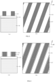
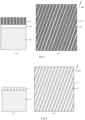
- FIGS. 1 to 2 are schematic structural diagrams corresponding to various steps in a method of manufacturing a semiconductor structure. Referring to FIG. 1 , a base 30 is provided and stripe-shaped first mask layers 31 are formed on the base 30. Referring to FIG. 2 , the first mask layers 31 (referring to FIG.
- the first sub-mask layers 311 are a mask layer to subsequently form active regions.
- the first sub-mask layers 311 are a plurality of discrete structures, and there are no other structures to fix and support the first sub-mask layers 311. Therefore, in an etching process, the first sub-mask layers 311 are prone to shift and tilt.
- the base 30 is etched by using the first sub-mask layers 311 as a mask, to form the active regions. There is no structure to fix the first sub-mask layers 311 and the active regions, and there is a greater etching depth. Therefore, both the first sub-mask layers 311 and the active regions may collapse and tilt, thus reducing the yield of the semiconductor structure.
- the embodiments of the present disclosure provide a method of manufacturing a semiconductor structure, including: forming a plurality of discrete first mask layers and a plurality of discrete second mask layers on a base, wherein the first mask layers intersect the second mask layers, and each of the second mask layers spans a plurality of the first mask layers; cutting off the first mask layers to form a plurality of discrete first sub-mask layers, wherein the second mask layers each span a plurality of the first mask layers to achieve an effect of supporting and fixing the first mask layers, thus preventing the first sub-mask layers from displacement or tilt; etching the base by using the first sub-mask layers as a mask, to form discrete active regions, wherein the second mask layers can achieve an effect of fixing and supporting the first sub-mask layers, such that the first sub-mask layers do not collapse or shift in a process of etching the active regions, moreover, the first sub-mask layers are in contact with the active regions, such that the second mask layers can also achieve an effect of fixing and supporting the
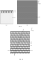
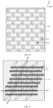
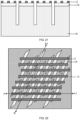
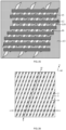
- FIGS. 3 to 25 are schematic structural diagrams corresponding to various steps in a method of manufacturing a semiconductor structure. The method of manufacturing a semiconductor structure is specifically described below with reference to the drawings.
- a base 10 is provided, and a plurality of discrete first mask layers 11 and a plurality of discrete second mask layers 12 are formed on the base 10.
- the first mask layers 11 each extend along a first direction X
- the second mask layers 12 each extend along a second direction Y
- the first direction X is different from the second direction Y.
- the first mask layers 11 intersect the second mask layers 12, and the second mask layers 12 each span a plurality of the first mask layers 11.
- a material of the base 10 may be a semiconductor, and a material type of the base 10 may be an elemental semiconductor material or a crystalline inorganic compound semiconductor material.
- the elemental semiconductor material may be silicon or germanium; and the crystalline inorganic compound semiconductor material may be silicon germanium, gallium arsenide, indium gallium or the like.
- An included angle between the first direction X and the second direction Y is 60° to 70°, the first direction X is an extension direction of the subsequently formed active regions, and the second direction Y is an extension direction of subsequently formed word line.
- the second mask layers 12 each span a plurality of the first mask layers 11, that is, the second mask layers 12 are in contact with at least sidewalls of the first mask layers 11. In this way, the second mask layers 12 may each achieve an effect of supporting a plurality of the first mask layers 11 through adhesion of contact surfaces therebetween.
- the second mask layers 12 can fix the first sub-mask layers to prevent tilt or displacement.
- the second mask layers 12 can also achieve an effect of fixing and supporting the active regions to prevent tilt or collapse.
- first mask layers 11 and the second mask layers 12 are described in detail below.
- the first mask layers 11 are formed before the second mask layers 12.
- the second mask layers may also be formed before the first mask layers.
- the first mask layers 11 are formed on the base 10.
- FIG. 3(a) is a partial cross-sectional diagram of FIG. 3(b) in the direction Y
- FIG. 3(b) is a top view of the semiconductor structure.
- An initial first mask layer 111 is formed on the base 10 and covers an entire upper surface of the base 10.
- the initial first mask layer 111 is a hard mask.
- a material of the initial first mask layer 111 is polysilicon.
- the material of the initial first mask layer may also be silicon oxide, silicon nitride or silicon carbide.
- the initial first mask layer 111 may be formed through chemical vapor deposition.
- Discrete seventh mask layers 117 are formed on the initial first mask layer 111, and the seventh mask layers 117 each extend along the first direction X.
- the seventh mask layers 117 are single-layer structures. In other embodiments, the seventh mask layers may also be double-layer structures, thus improving the precision of pattern transfer.
- the seventh mask layers 117 are hard masks, and a material thereof may be polysilicon, silicon oxide, silicon nitride or silicon carbide.
- forming the seventh mask layers 117 includes: forming an initial seventh mask layer on an upper surface of the initial first mask layer 111; and patterning the initial seventh mask layer to form the seventh mask layers 117, which each extend along the first direction X.
- the initial seventh mask layer may be formed through chemical vapor deposition, and may also be patterned through dry etching.
- an initial eighth mask layer covering the initial first mask layer may also be formed before the seventh mask layers are formed, and the initial eighth mask layer may improve the precision of pattern transfer.
- the initial eighth mask layer may be a single-layer or double-layer structure, and a material thereof may be silicon nitride, silicon carbide or silicon oxynitride.
- FIG. 4(a) is a partial cross-sectional diagram of FIG. 4(b) in the direction Y
- FIG. 4(b) is a top view of the semiconductor structure.
- a first sidewall layer 112 is formed on each sidewall of the seventh mask layers 117.
- the seventh mask layer 117 has a greater width than the first sidewall layer 112.
- the first sidewall layers 112 are hard masks, and a material thereof is different from the material of the seventh mask layers 117 and may be polysilicon, silicon oxide, silicon nitride or silicon carbide.
- the first sidewall layers 112 may be formed through an atomic layer deposition process or a chemical vapor deposition process.
- FIG. 5(a) is a partial cross-sectional diagram of FIG. 5(b) in the direction Y
- FIG. 5(b) is a top view of the semiconductor structure.
- the seventh mask layers 117 (referring to FIG. 4 ) are removed and the first sidewall layers 112 are retained.
- the seventh mask layers 117 may be removed through wet etching. In other embodiments, the seventh mask layers may also be removed through dry etching.
- FIG. 6(a) is a partial cross-sectional diagram of FIG. 6(b) in the direction Y
- FIG. 6(b) is a top view of the semiconductor structure.
- a second sidewall layer 113 is formed on each sidewall of the first sidewall layers 112.
- the second sidewall layers 113 are hard masks, and a material thereof is different from the material of the first sidewall layers 112 and may be polysilicon, silicon oxide, silicon nitride or silicon carbide.
- the second sidewall layers 113 may be formed through the atomic layer deposition process or the chemical vapor deposition process.
- the initial eighth mask layer may be formed on the initial first mask layer.
- the initial eighth mask layer may be etched by using the first sidewall layers as a mask, to form a plurality of discrete eighth mask layers, thus transferring patterns of the first sidewall layers to the eighth mask layers.
- a second sidewall layer may also be formed on each sidewall of the eighth mask layers.
- FIG. 7(a) is a partial cross-sectional diagram of FIG. 7(b) in the direction Y
- FIG. 7(b) is a top view of the semiconductor structure.
- the first sidewall layers 112 (referring to FIG. 6 ) are removed, and the second sidewall layers 113 are retained.
- the first sidewall layers 112 may be removed through wet etching. In other embodiments, the first sidewall layers may also be removed through dry etching.
- a plurality of discrete eighth mask layers may be formed and a second sidewall layer is formed on each sidewall of the eighth mask layers.
- the eighth mask layers may be removed after the second sidewall layers are formed.
- FIG. 8(a) is a partial cross-sectional diagram of FIG. 8(b) in the direction Y
- FIG. 8(b) is a top view of the semiconductor structure.
- the initial first mask layer 111 (referring to FIG. 7 ) is etched by using the second sidewall layers 113 (referring to FIG. 7 ) as a mask, to form the first mask layers 11.
- the first mask layers 11 are stripe-shaped masks, which each extend along the first direction X, and the first mask layers 11 also expose partial upper surface of the base 10.
- the first mask layers 11 are hard mask layers.
- a material of the first mask layers 11 is polysilicon.
- the material of the first mask layers 11 may also be silicon oxide, silicon nitride or silicon carbide.
- the hard mask layer has higher hardness and strength, such that the effect of the subsequently formed second mask layers for supporting and fixing the first mask layers may be improved.
- FIG. 9(a) is a partial cross-sectional diagram of FIG. 9(b) in the direction Y
- FIG. 9(b) is a top view of the semiconductor structure.
- An initial second mask layer 121 located between adjacent first mask layers 11 is formed.
- the initial second mask layer 121 is also located on the first mask layers 11. That is, a top surface of the initial second mask layer 121 is higher than top surfaces of the first mask layers 11. It is understandable that, when the initial second mask layer 121 is still located on the first mask layers 11, the initial second mask layer 121 is also in contact with the top surfaces of the first mask layers 11. In this way, a contact area therebetween may be increased to increase the adhesion of the first mask layers 11 on a contact surface, thus improving the effect of the subsequently formed second mask layers for supporting the first mask layers 11.
- the initial second mask layer may be located only between adjacent first mask layers. That is, the top surface of the initial second mask layer is flush with the top surfaces of the first mask layers or lower than the top surfaces of the first mask layers.
- the initial second mask layer 121 is a hard mask layer, and a material thereof is different from the material of the first mask layers 11.
- the material of the initial second mask layer 121 may be silicon carbide.
- the material of the initial second mask layer may also be silicon nitride, silicon oxide or silicon carbonitride.
- FIG. 11 is a cross-sectional diagram of FIG. 10 in an A-A1 direction
- FIG. 12 is a cross-sectional diagram of FIG. 10 in a B-B1 direction.
- the initial second mask layer 121 (referring to FIG. 9 ) is patterned by using a second etching process, to form the second mask layers 12.
- the second etching process has a higher etch selectivity for the initial second mask layer 121 and the first mask layers 11. In this way, in the process of etching the initial second mask layer 121, the first mask layers 11 are less damaged by the second etching process, thus maintaining the original shape of the first mask layers 11 and ensuring the precision of patterns of the subsequently formed active regions.
- the material of the initial second mask layer 121 is silicon carbide.
- an etching gas of the second etching process includes O 2 and Ar.
- the initial second mask layer 121 (referring to FIG. 9 ) is also located on the first mask layers 11.
- top surfaces of the second mask layers 12 are higher than the top surfaces of the first mask layers 11. It is understandable that, when the top surfaces of the second mask layers 12 are higher than the top surfaces of the first mask layers 11, the plurality of discrete second mask layers 12 located between adjacent first mask layers 11 are connected into a whole through the second mask layers 12 higher than the top surfaces of the first mask layers 11.
- the second mask layers 12 are not only in contact with the sidewalls of the first mask layers 11, but also in contact with the top surfaces of the first mask layers 11.
- the second mask layers 12 may achieve an effect of hauling and fixing the first mask layers 11 through the sidewalls and the top surfaces of the first mask layers 11, thus preventing the first sub-mask layers from displacement or tilt in a subsequent process of forming the first sub-mask layers.
- the first sub-mask layers are also in contact with the base 10, such that in a subsequent process of etching the base 10 to form the active regions, the second mask layers 12 may also achieve an effect of fixing and supporting the active regions through the first sub-mask layers, thus preventing the active regions from collapse or tilt.
- the second mask layers may also be located only between adjacent first mask layers. That is, the second mask layers are discrete block structures, and are in contact with only the sidewalls of the first mask layers. That is, the second mask layers may achieve the effect of supporting and fixing the first mask layers through the sidewalls of the first mask layers.
- the second mask layers 12 are hard mask layers, which may further improve the strength of the second mask layers 12 for supporting the first mask layers 11. Therefore, the first mask layers 11 and the subsequent active regions are prevented from tilt or collapse.
- the first mask layers 11 are cut off to form a plurality of discrete first sub-mask layers 118.
- the second mask layers 12 each span a plurality of the first sub-mask layers 118, and partial sidewalls of each of the first sub-mask layers 118 are covered by the second mask layers 12.
- the second mask layers 12 are in contact with a central region and two edge regions of each of the first sub-mask layers 118.
- each of the first sub-mask layers 118 is in contact with three second mask layers 12 (the first mask layers 11 and the second mask layers 12 that are located at edges in the figure are not shown).
- the second mask layers 12 intersect the plurality of first sub-mask layers 118. Therefore, in the process of forming the first sub-mask layers 118, the second mask layers 12 may fix and support the plurality of first sub-mask layers 118, thus preventing the first sub-mask layers 118 from tilt or displacement.
- the discrete first sub-mask layers 118 are used as a mask layer to subsequently form the active regions.
- the first sub-mask layers 118 are fixed by the second mask layers 12, thus improving the precision of the subsequently formed active regions.
- the first sub-mask layers 118 are also in contact with the active regions, such that the second mask layers 12 may also support and fix the active regions through the first sub-mask layers 118, thus preventing the active regions from tilt or collapse.
- Forming the first sub-mask layers 118 is described in detail below.
- fifth mask layer 191 is formed on the first mask layers 11, and is patterned to form second trenches 196 exposing the first mask layers 11 and the second mask layers 12. That is, the patterned fifth mask layer 191 may be formed through one-time photolithography.
- the patterned fifth mask layer 191 is stripe-shaped structures, and spans the plurality of first mask layers 11.
- the second trenches 196 expose to-be-cut regions of the plurality of first mask layers 11. The first mask layers 11 located in the to-be-cut regions are subsequently removed.
- partial material of the fifth mask layer 191 is filled between adjacent first mask layers 11 and between adjacent second mask layers 12.
- the material of the fifth mask layer 191 filled between adjacent first mask layers 11 and between adjacent second mask layers 12 is also removed.
- the fifth mask layer 191 exposing all the to-be-cut regions of the first mask layers 11 is formed through a one-time photolithography process.
- an upper mask layer and a lower mask layer may also be formed through a twice photolithography process.
- the upper mask layer corresponds to one part of the to-be-cut regions of the first mask layers
- the lower mask layer corresponds to the other part of the to-be-cut regions of the first mask layers.
- the fifth mask layer 191 is formed on the first mask layers 11, and is patterned to form discrete cutoff holes exposing the first mask layers 11.
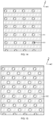
- the cutoff holes include first cutoff holes 193 and second cutoff holes 194. For each of the first mask layers 11, orthographic projections of the first cutoff holes 193 and the second cutoff holes 194 on the top surface of the first mask layer 11 are alternately arranged.
- Forming the cutoff holes is as follows: referring to FIG. 14 , first patterning is performed on the fifth mask layer 191 to form the first cutoff holes 193; a first photoresist layer is formed on the fifth mask layer 191, and is exposed and shadowed to form patterned first photoresist layer; the fifth mask layer 191 is etched by using the patterned first photoresist layer as a mask, to form the first cutoff holes 193; and after the first cutoff holes 193 are formed, the patterned first photoresist layer is removed. Referring to FIG. 14 , first patterning is performed on the fifth mask layer 191 to form the first cutoff holes 193; a first photoresist layer is formed on the fifth mask layer 191, and is exposed and shadowed to form patterned first photoresist layer; the fifth mask layer 191 is etched by using the patterned first photoresist layer as a mask, to form the first cutoff holes 193; and after the first cutoff holes 193 are formed, the patterned first photoresist
- a sixth mask layer 192 is formed on the fifth mask layer 191, and is patterned to form initial second cutoff holes; a second photoresist layer is formed on the sixth mask layer 192, and is exposed and shadowed to form patterned second photoresist layer; the sixth mask layer 192 is etched by using the patterned second photoresist layer as a mask, to form a patterned sixth mask layer 192; and after the patterned sixth mask layer 192 is formed, the second photoresist layer is removed. Referring to FIG.
- second patterning is performed on the fifth mask layer 191 by using the patterned sixth mask layer 192 as a mask, to form the second cutoff holes 194; and after the second cutoff holes 194 are formed, the sixth mask layer 192 is removed.
- the first cutoff holes 193 and the second cutoff holes 194 that are alternately arranged are formed on the fifth mask layer 191.
- the first mask layers 11 may be subsequently etched along the cutoff holes, to form the first sub-mask layers.
- FIG. 17 is a partial top view of the semiconductor structure
- FIG. 18 is a cross-sectional diagram of FIG. 17 in the A-A1 direction
- FIG. 19 is a cross-sectional diagram of FIG. 17 in the B-B1 direction.
- the first mask layers 11 are etched by using the fifth mask layer 191 as a mask, to form the first sub-mask layers 118.
- the second mask layers 12 may achieve the effect of hauling and fixing the first sub-mask layers 118, such that the first sub-mask layers 118 may be prevented from shift and displacement and benefit is brought to improve the precision of the patterns of the subsequently formed active regions.
- the first mask layers 11 are cut off through dry etching.
- the material of the first mask layers 11 is polysilicon.
- an etching gas may be SF 6 , CF 4 or Cl 2 .
- FIG. 20 is a cross-sectional diagram of Fig. 17 in the A-A1 direction
- FIG. 21 is a cross-sectional diagram of FIG. 17 in the B-B1 direction.
- the base 10 is etched through a first etching process by using the first sub-mask layers 118 as a mask, to form the discrete active regions 119.
- the first etching process is plasma etching. According to the plasma etching, parts of the base 10 are removed through ion beams.
- the first etching process may be divided into two stages. In the first stage, a direction of the ion beams is perpendicular to the top surface of the base 10. That is, the ion beams tilt 90° toward a bottom of the base along the first direction X, to remove parts of the base 10 not shielded by the first sub-mask layers 118 and the second mask layers 12.
- the ion beams tilt 0° to 30° toward the bottom of the base along the first direction X, to remove parts of the base 10 located right below the second mask layers 12, and the base 10 located right below the first sub-mask layers 118 is retained to form the plurality of mutually independent active regions 119.
- the ion beams may etch sidewalls of the active regions 119 along the first direction X.
- a thickness of the first sub-mask layers 118 may be suitably increased. That is, a loss allowance is previously stored for the active regions 119, and the loss allowance stored in the previous step may be removed through the plasma etching in the second stage.
- sequences of the first stage and the second stage may also be exchanged, or there may be only the second stage.
- the second mask layers 12 may haul and fix the active regions 119 through the first sub-mask layers 118. In this way, in the process of forming the active regions 119, the active regions 119 may be prevented from tilt or collapse, thus improving the yield of the semiconductor structure.
- An etch selectivity of the first etching process for the base 10 and the second mask layers 12 is greater than 10, for example, 12, 20 or 50.
- the first etching process may be prone to remove parts of the base 10 to form the discrete active regions 119, and may also prevent the second mask layers 12 from being excessively damaged, thus improving the effect of the second mask layers 12 for supporting the active regions 119.
- An etching gas of the first etching process may be SF 6 , CF 4 , Cl 2 , CHF 3 , O 2 , Ar or mixed gas thereof.
- FIG. 23 is a cross-sectional diagram of FIG. 22 in the A-A1 direction
- FIG. 24 is a cross-sectional diagram of FIG. 22 in the B-B1 direction.
- a isolation structure 13 located between adjacent active regions 119 is formed, and the first sub-mask layers 118 not covered by the second mask layers 12 are removed.
- the isolation structure 13 may be formed through a chemical vapor deposition method. In other embodiments, the isolation structure may also be formed through a physical vapor deposition method.
- a material of the isolation structure 13 may be silicon oxide, silicon nitride or silicon oxynitride.
- the first sub-mask layers 118 not covered by the second mask layers 12 are removed. That is, the first sub-mask layers 118 located in the second mask layers 12 are retained. In the embodiment, a part of each of the first sub-mask layers 118 may be removed through dry etching.
- third mask layers 15 are formed on two opposite sidewalls of each of the second mask layers 12.
- the active regions 119 and the isolation structure 13 are etched by using the second mask layers 12 and the third mask layers 15 as a mask, to form a word line trench 16.
- the third mask layers 15 are formed before the active regions 119 and the isolation structure 13 are etched.
- the third mask layers 15 are used to finely adjust positions and sizes of the word line trench 16.
- the third mask layers 15 are not formed. That is, the third mask layers 15 do not shield a part of each of the to-be-cut regions of the first mask layers 11. In this way, the difficulty of cutting off the first mask layers 11 may be reduced by a larger process window.
- a ratio of a width of the second mask layer 12 to a width of the third mask layer 15 is 4: 1 to 6: 1. It is understandable that, if the width of the second mask layer 12 is excessively large, the difficulty of cutting off the first mask layers 11 may be increased; and if the width of the second mask 12 is excessively small, the effect of the second mask layers 12 for supporting and fixing the first mask layers 11 may be reduced.
- the ratio of the width of the second mask layer 12 to the width of the third mask layer 15 is 4: 1 to 6: 1, the precision of a size of the word line trench can be ensured. Meanwhile, the difficulty of cutting off the first mask layers 11 can be reduced, and the effect of the second mask layers 12 for supporting the first mask layers 11 can be improved.
- the third mask layers may also not be formed on the sidewalls of the second mask layers.
- the width of the third mask layer in the direction perpendicular to the second direction Y may be increased.
- the active regions and the isolation structure may be directly etched by using the second mask layers as a mask.
- a word line filling the word line trench 16 is formed.
- the first mask layers 11 intersect the second mask layers 12. Therefore, in the process of cutting off the first mask layers 11, the second mask layers 12 may achieve the effect of supporting and fixing the first mask layers 11, thus preventing the first sub-mask layers 118 from displacement or tilt. Moreover, the first sub-mask layers 118 are in contact with the active regions 119. In this way, the second mask layers 12 may achieve the effect of fixing and supporting the active regions 119 through the first sub-mask layers 118, thus preventing the active regions from shift or collapse and improving the yield of the semiconductor structure.
- the second mask layers 12 are also used as a mask layer to form the word line trench 16, thus simplifying the production process.
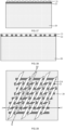
- FIGS. 26 to 31 are schematic structural diagrams corresponding to various steps of a method of manufacturing a semiconductor structure according to the embodiment of the present disclosure.
- FIG. 27 is a cross-sectional diagram of FIG. 26 in the A-A1 direction
- FIG. 28 is a cross-sectional diagram of FIG. 26 in the B-B1 direction.
- a base 20 is provided, and a plurality of discrete first mask layers 21 and a plurality of discrete second mask layers 22 are formed on the base 20.
- the first mask layers 21 each extend along a first direction X
- the second mask layers 22 each extend along a second direction Y
- the first direction X is different from the second direction Y.
- the first mask layers 21 intersect the second mask layers 22, and the second mask layers 22 each span a plurality of the first mask layers 21.
- Forming the second mask layers 22 is as follows: an initial second mask layer which is a whole mask layer covering the base is formed on the base 20; and the initial second mask layer is patterned to form the discrete second mask layers.
- an initial second mask layer which is a whole mask layer covering the base is formed on the base 20; and the initial second mask layer is patterned to form the discrete second mask layers.
- Forming the first mask layers 21 are as follows: an initial first mask layer located between adjacent second mask layers 22 is formed, and discrete seventh mask layers are formed on the initial first mask layer, wherein the seventh mask layers each extend along the first direction; a first sidewall layer is formed on each sidewall of the seventh mask layers; the seventh mask layers are removed, and a second sidewall layer is formed on each sidewall of the first sidewall layers; and the first sidewall layers are removed, and the initial first mask layer is etched by using the second sidewall layers as a mask, to form the first mask layers.
- the first mask layers refer to detailed description in the previous embodiment.
- the initial first mask layer is also located on the second mask layers 22.
- the first mask layers 21 are also located on the second mask layers 22. That is, top surfaces of the first mask layers 21 are higher than top surfaces of the second mask layers 22, and the fist mask layers 21 are in contact with sidewalls and the top surfaces of the second mask layers 22. Therefore, the second mask layers 22 may achieve an effect of supporting the plurality of first mask layers 21 through the sidewalls and the top surfaces.
- the second mask layers 22 can fix the first sub-mask layers to prevent tilt or displacement.
- the second mask layers 22 can also achieve an effect of fixing and supporting the active regions to prevent tilt or collapse.
- the initial first mask layer may also be located only between two adjacent second mask layers.
- the first mask layers are located only between two opposite sidewalls of each of the second mask layers. That is, the top surfaces of the first mask layers are flush with or lower than the top surfaces of the second mask layers.
- sidewalls of the first mask layers in contact with the second mask layers also have adhesion, such that the second mask layers may support and fix the first mask layers through the sidewalls.
- FIG. 30 is a cross-sectional diagram of FIG. 29 in the A-A1 direction
- FIG. 31 is a cross-sectional diagram of FIG. 29 in the B-B1 direction.
- the first mask layers 21 are cut off to form a plurality of discrete first sub-mask layers 218.
- the second mask layers 22 each span a plurality of the first sub-mask layers 218, and partial sidewalls of each of the first sub-mask layers 218 are covered by the second mask layers 22.
- first mask layers 21 are in contact with the top surfaces and sidewalls of the second mask layers 22, such that the second mask layers 22 may achieve an effect of fixing and supporting the first mask layers 21, thus preventing the first sub-mask layers 218 from shift or tilt.
- the base is etched through a first etching process by using the first sub-mask layers 218 as a mask, to form discrete active regions.
- the second mask layers 22 may support and fix the active regions through the first sub-mask layers 218, thus preventing the active regions from collapse or tilt.
- a isolation structure located between adjacent active regions is formed, and the first sub-mask layers 218 not covered by the second mask layers 22 are removed.
- the isolation structure and the active regions may be etched by using the second mask layers 22 as a mask, to form a word line trench.
- the second mask layers 22 are firstly formed, and then the first mask layers 21 are formed.
- the first mask layers 21 intersect the second mask layers 22, such that the second mask layers 22 may fix and support the subsequently formed first sub-mask layers 218 and the subsequently formed active regions, thus preventing the first sub-mask layers 218 and the active regions from collapse or tilt.
- the second mask layers are also used to form the word line trench, thus simplifying the production process.
- the second mask layers each span a plurality of first mask layers.
- the second mask layers can achieve the effect of supporting and fixing the first mask layers, thus preventing the first sub-mask layers from displacement or tilt.
- the first sub-mask layers are in contact with the active regions. Therefore, the second mask layers can also achieve the effect of fixing and supporting the active regions through the first sub-mask layers, thus preventing the active regions from shift or collapse.
- the active regions and the isolation structure are etched by using the second mask layers as a mask, to form the word line trench. That is, the second mask layers are also used as a mask layer to form the word line trench, thus simplifying the production process and improving the yield of the semiconductor structure.
Landscapes
- Semiconductor Memories (AREA)
- Drying Of Semiconductors (AREA)
Applications Claiming Priority (2)
| Application Number | Priority Date | Filing Date | Title |
|---|---|---|---|
| CN202110553933.3A CN115377011A (zh) | 2021-05-20 | 2021-05-20 | 半导体结构的制造方法 |
| PCT/CN2021/120125 WO2022241994A1 (zh) | 2021-05-20 | 2021-09-24 | 半导体结构的制造方法 |
Publications (3)
| Publication Number | Publication Date |
|---|---|
| EP4220699A1 true EP4220699A1 (de) | 2023-08-02 |
| EP4220699A4 EP4220699A4 (de) | 2024-05-22 |
| EP4220699B1 EP4220699B1 (de) | 2026-05-06 |
Family
ID=82802945
Family Applications (1)
| Application Number | Title | Priority Date | Filing Date |
|---|---|---|---|
| EP21940441.5A Active EP4220699B1 (de) | 2021-05-20 | 2021-09-24 | Herstellungsverfahren für eine dram struktur |
Country Status (2)
| Country | Link |
|---|---|
| US (1) | US11417533B1 (de) |
| EP (1) | EP4220699B1 (de) |
Cited By (1)
| Publication number | Priority date | Publication date | Assignee | Title |
|---|---|---|---|---|
| TWI892686B (zh) * | 2023-11-14 | 2025-08-01 | 南亞科技股份有限公司 | 包含切割結構的半導體元件的製備方法 |
Family Cites Families (10)
| Publication number | Priority date | Publication date | Assignee | Title |
|---|---|---|---|---|
| KR101658492B1 (ko) | 2010-08-13 | 2016-09-21 | 삼성전자주식회사 | 미세 패턴의 형성 방법 및 이를 이용한 반도체 소자의 제조 방법 |
| KR101096166B1 (ko) | 2010-12-17 | 2011-12-19 | 주식회사 하이닉스반도체 | 반도체 장치 및 그 제조방법 |
| KR101974350B1 (ko) | 2012-10-26 | 2019-05-02 | 삼성전자주식회사 | 활성 영역을 한정하는 라인 형 트렌치들을 갖는 반도체 소자 및 그 형성 방법 |
| KR20150131450A (ko) * | 2014-05-14 | 2015-11-25 | 삼성전자주식회사 | 반도체 소자 및 그 제조방법 |
| KR102265271B1 (ko) | 2015-01-14 | 2021-06-17 | 삼성전자주식회사 | 반도체 소자 및 그 제조방법 |
| KR102280471B1 (ko) * | 2015-07-20 | 2021-07-22 | 삼성전자주식회사 | 액티브 패턴들 형성 방법, 액티브 패턴 어레이, 및 반도체 장치 제조 방법 |
| KR102420150B1 (ko) | 2015-08-19 | 2022-07-13 | 삼성전자주식회사 | 반도체 소자의 제조 방법 |
| US11289487B2 (en) | 2018-02-23 | 2022-03-29 | Micron Technology, Inc. | Doped titanium nitride materials for DRAM capacitors, and related semiconductor devices, systems, and methods |
| CN121013339A (zh) | 2019-09-27 | 2025-11-25 | 福建省晋华集成电路有限公司 | 半导体器件 |
| CN112786444B (zh) | 2019-11-08 | 2024-12-10 | 长鑫存储技术有限公司 | 存储器及其形成方法 |
-
2021
- 2021-09-24 EP EP21940441.5A patent/EP4220699B1/de active Active
-
2022
- 2022-01-21 US US17/648,558 patent/US11417533B1/en active Active
Cited By (1)
| Publication number | Priority date | Publication date | Assignee | Title |
|---|---|---|---|---|
| TWI892686B (zh) * | 2023-11-14 | 2025-08-01 | 南亞科技股份有限公司 | 包含切割結構的半導體元件的製備方法 |
Also Published As
| Publication number | Publication date |
|---|---|
| EP4220699B1 (de) | 2026-05-06 |
| US11417533B1 (en) | 2022-08-16 |
| EP4220699A4 (de) | 2024-05-22 |
Similar Documents
| Publication | Publication Date | Title |
|---|---|---|
| KR100874196B1 (ko) | 마스크 물질 변환 | |
| CN103794475B (zh) | 自对准三重图形化方法 | |
| KR20050062019A (ko) | 실리콘 기판과 식각 선택비가 큰 마스크층을 이용한리세스 채널 어레이 트랜지스터의 제조 방법 | |
| KR20130007678A (ko) | 반도체 구조체 | |
| US11887859B2 (en) | Method for forming active region array and semiconductor structure | |
| KR102824282B1 (ko) | 미세 패턴의 절단 방법, 이를 이용한 액티브 패턴들의 형성 방법, 및 이를 이용한 반도체 장치의 제조 방법 | |
| US20240049456A1 (en) | Semiconductor structure and preparation method thereof | |
| US20090117742A1 (en) | Method for fabricating fine pattern in semiconductor device | |
| US11417533B1 (en) | Manufacturing method of semiconductor structure | |
| CN111668093B (zh) | 半导体器件及其形成方法 | |
| US7648878B2 (en) | Method for fabricating semiconductor device with recess gate | |
| WO2022148004A1 (zh) | 位线接触结构的形成方法及半导体结构 | |
| CN111640667B (zh) | 半导体器件及其形成方法 | |
| CN111668099B (zh) | 图形化方法及其形成的半导体器件 | |
| CN113363142A (zh) | 半导体器件的形成方法 | |
| CN115223863B (zh) | 半导体结构的制作方法 | |
| US11894231B2 (en) | Semiconductor fabrication method and structure using multiple sacrificial layers to form sidewall spacers | |
| WO2022241994A1 (zh) | 半导体结构的制造方法 | |
| CN111640664B (zh) | 半导体器件及其形成方法 | |
| US12532713B2 (en) | Method for manufacturing semiconductor device | |
| CN113972163A (zh) | 半导体器件的隔离的形成方法 | |
| CN115394634A (zh) | 半导体结构的制造方法 | |
| TWI871007B (zh) | 半導體結構及其形成方法 | |
| US12100593B2 (en) | Method for forming self-aligned double pattern and semiconductor structures | |
| KR20020002574A (ko) | 반도체 소자의 콘택플러그 형성방법 |
Legal Events
| Date | Code | Title | Description |
|---|---|---|---|
| STAA | Information on the status of an ep patent application or granted ep patent |
Free format text: STATUS: THE INTERNATIONAL PUBLICATION HAS BEEN MADE |
|
| PUAI | Public reference made under article 153(3) epc to a published international application that has entered the european phase |
Free format text: ORIGINAL CODE: 0009012 |
|
| STAA | Information on the status of an ep patent application or granted ep patent |
Free format text: STATUS: REQUEST FOR EXAMINATION WAS MADE |
|
| 17P | Request for examination filed |
Effective date: 20230424 |
|
| AK | Designated contracting states |
Kind code of ref document: A1 Designated state(s): AL AT BE BG CH CY CZ DE DK EE ES FI FR GB GR HR HU IE IS IT LI LT LU LV MC MK MT NL NO PL PT RO RS SE SI SK SM TR |
|
| REG | Reference to a national code |
Ref country code: DE Ref legal event code: R079 Free format text: PREVIOUS MAIN CLASS: H01L0021824200 Ipc: H10B0012000000 Ref country code: DE Ref legal event code: R079 Ref document number: 602021054143 Country of ref document: DE Free format text: PREVIOUS MAIN CLASS: H01L0021824200 Ipc: H10B0012000000 |
|
| A4 | Supplementary search report drawn up and despatched |
Effective date: 20240418 |
|
| RIC1 | Information provided on ipc code assigned before grant |
Ipc: H01L 21/762 20060101ALI20240412BHEP Ipc: H01L 21/308 20060101ALI20240412BHEP Ipc: H10B 12/00 20230101AFI20240412BHEP |
|
| DAV | Request for validation of the european patent (deleted) | ||
| DAX | Request for extension of the european patent (deleted) | ||
| GRAP | Despatch of communication of intention to grant a patent |
Free format text: ORIGINAL CODE: EPIDOSNIGR1 |
|
| STAA | Information on the status of an ep patent application or granted ep patent |
Free format text: STATUS: GRANT OF PATENT IS INTENDED |
|
| RIC1 | Information provided on ipc code assigned before grant |
Ipc: H10B 12/00 20230101AFI20260115BHEP Ipc: H10P 50/00 20260101ALI20260115BHEP Ipc: H10W 10/17 20260101ALI20260115BHEP |
|
| INTG | Intention to grant announced |
Effective date: 20260123 |
|
| GRAS | Grant fee paid |
Free format text: ORIGINAL CODE: EPIDOSNIGR3 |
|
| GRAA | (expected) grant |
Free format text: ORIGINAL CODE: 0009210 |
|
| STAA | Information on the status of an ep patent application or granted ep patent |
Free format text: STATUS: THE PATENT HAS BEEN GRANTED |
|
| P01 | Opt-out of the competence of the unified patent court (upc) registered |
Free format text: CASE NUMBER: UPC_APP_0009311_4220699/2026 Effective date: 20260311 |