EP4224542A1 - Piezoelektrischer aktor - Google Patents
Piezoelektrischer aktor Download PDFInfo
- Publication number
- EP4224542A1 EP4224542A1 EP21874955.4A EP21874955A EP4224542A1 EP 4224542 A1 EP4224542 A1 EP 4224542A1 EP 21874955 A EP21874955 A EP 21874955A EP 4224542 A1 EP4224542 A1 EP 4224542A1
- Authority
- EP
- European Patent Office
- Prior art keywords
- piezoelectric element
- lead
- recessed
- piezoelectric
- piezoelectric actuator
- Prior art date
- Legal status (The legal status is an assumption and is not a legal conclusion. Google has not performed a legal analysis and makes no representation as to the accuracy of the status listed.)
- Pending
Links
Images





Classifications
-
- H—ELECTRICITY
- H10—SEMICONDUCTOR DEVICES; ELECTRIC SOLID-STATE DEVICES NOT OTHERWISE PROVIDED FOR
- H10N—ELECTRIC SOLID-STATE DEVICES NOT OTHERWISE PROVIDED FOR
- H10N30/00—Piezoelectric or electrostrictive devices
- H10N30/50—Piezoelectric or electrostrictive devices having a stacked or multilayer structure
-
- H—ELECTRICITY
- H10—SEMICONDUCTOR DEVICES; ELECTRIC SOLID-STATE DEVICES NOT OTHERWISE PROVIDED FOR
- H10N—ELECTRIC SOLID-STATE DEVICES NOT OTHERWISE PROVIDED FOR
- H10N30/00—Piezoelectric or electrostrictive devices
- H10N30/50—Piezoelectric or electrostrictive devices having a stacked or multilayer structure
- H10N30/508—Piezoelectric or electrostrictive devices having a stacked or multilayer structure adapted for alleviating internal stress, e.g. cracking control layers
-
- H—ELECTRICITY
- H10—SEMICONDUCTOR DEVICES; ELECTRIC SOLID-STATE DEVICES NOT OTHERWISE PROVIDED FOR
- H10N—ELECTRIC SOLID-STATE DEVICES NOT OTHERWISE PROVIDED FOR
- H10N30/00—Piezoelectric or electrostrictive devices
- H10N30/20—Piezoelectric or electrostrictive devices with electrical input and mechanical output, e.g. functioning as actuators or vibrators
- H10N30/206—Piezoelectric or electrostrictive devices with electrical input and mechanical output, e.g. functioning as actuators or vibrators using only longitudinal or thickness displacement, e.g. d33 or d31 type devices
-
- H—ELECTRICITY
- H10—SEMICONDUCTOR DEVICES; ELECTRIC SOLID-STATE DEVICES NOT OTHERWISE PROVIDED FOR
- H10N—ELECTRIC SOLID-STATE DEVICES NOT OTHERWISE PROVIDED FOR
- H10N30/00—Piezoelectric or electrostrictive devices
- H10N30/80—Constructional details
- H10N30/87—Electrodes or interconnections, e.g. leads or terminals
- H10N30/871—Single-layered electrodes of multilayer piezoelectric or electrostrictive devices, e.g. internal electrodes
-
- H—ELECTRICITY
- H10—SEMICONDUCTOR DEVICES; ELECTRIC SOLID-STATE DEVICES NOT OTHERWISE PROVIDED FOR
- H10N—ELECTRIC SOLID-STATE DEVICES NOT OTHERWISE PROVIDED FOR
- H10N30/00—Piezoelectric or electrostrictive devices
- H10N30/80—Constructional details
- H10N30/87—Electrodes or interconnections, e.g. leads or terminals
- H10N30/872—Interconnections, e.g. connection electrodes of multilayer piezoelectric or electrostrictive devices
-
- H—ELECTRICITY
- H10—SEMICONDUCTOR DEVICES; ELECTRIC SOLID-STATE DEVICES NOT OTHERWISE PROVIDED FOR
- H10N—ELECTRIC SOLID-STATE DEVICES NOT OTHERWISE PROVIDED FOR
- H10N30/00—Piezoelectric or electrostrictive devices
- H10N30/80—Constructional details
- H10N30/87—Electrodes or interconnections, e.g. leads or terminals
- H10N30/875—Further connection or lead arrangements, e.g. flexible wiring boards, terminal pins
-
- H—ELECTRICITY
- H10—SEMICONDUCTOR DEVICES; ELECTRIC SOLID-STATE DEVICES NOT OTHERWISE PROVIDED FOR
- H10N—ELECTRIC SOLID-STATE DEVICES NOT OTHERWISE PROVIDED FOR
- H10N30/00—Piezoelectric or electrostrictive devices
- H10N30/80—Constructional details
- H10N30/88—Mounts; Supports; Enclosures; Casings
Definitions
- the present disclosure relates to a piezoelectric actuator.
- a known piezoelectric actuator includes a piezoelectric element and a metal case.
- the piezoelectric element is layered in a pillar shape.
- the metal case accommodates the piezoelectric element so that both end portions of the piezoelectric element are in contact with an inner wall of the metal case (for example, see Patent Document 1).
- an electrode plate is bonded to a side surface of a piezoelectric element having a columnar shape.
- a drive voltage is applied to the piezoelectric element via the electrode plate.
- the electrode plate includes a body portion bonded to the side surface of the piezoelectric element and a lead portion electrically connecting the body portion and a lead terminal.
- Patent Document 1 JP 2013-211419 A
- An aspect of the embodiment provides a piezoelectric actuator capable of suppressing peeling of an electrode plate from a piezoelectric element.
- a piezoelectric actuator includes a piezoelectric element layered in a pillar shape, and an electrode plate located on a side surface of the piezoelectric element and being electrically connected to an internal electrode layer of the piezoelectric element.
- the electrode plate includes a body portion extending in a layering direction of the piezoelectric element, and a lead portion extending in a direction intersecting the layering direction and being electrically connected to a lead terminal.
- the lead portion includes, in at least one side portion thereof, a recessed portion recessed in a width direction of the lead portion.
- a known piezoelectric actuator includes a piezoelectric element and a metal case.
- the piezoelectric element is layered in a pillar shape.
- the metal case accommodates the piezoelectric element so that both end portions of the piezoelectric element are in contact with an inner wall of the metal case.
- an electrode plate is bonded to a side surface of a piezoelectric element having a columnar shape.
- a drive voltage is applied to the piezoelectric element via the electrode plate.
- the electrode plate includes a body portion bonded to the side surface of the piezoelectric element and a lead portion electrically connecting the body portion and a lead terminal.
- the lead portion may be unable to sufficiently deform with respect to an expansion and contraction operation of the piezoelectric element, and the body portion may peel from the piezoelectric element.
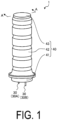
- FIG. 1 is a perspective view illustrating the overall configuration of the piezoelectric actuator 1 according to the embodiment
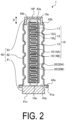
- FIG. 2 is an arrow cross-sectional view taken along an A-A line illustrated in FIG. 1
- FIG. 3 is a perspective view illustrating a configuration of an inner portion of the piezoelectric actuator 1 according to the embodiment.
- the piezoelectric actuator 1 includes a piezoelectric element 10, a pair of electrode plates 20, a pair of lead terminals 30, and a case 40.
- the pair of electrode plates 20 includes an electrode plate 20A and an electrode plate 20B.
- the pair of lead terminals 30 includes a lead terminal 30A and a lead terminal 30B.
- the piezoelectric element 10 has a pillar shape.
- the piezoelectric element 10 has a quadrangular pillar shape (rectangular parallelepiped shape) having a length of from 0.5 (mm) to 10 (mm), a width of from 0.5 (mm) to 10 (mm), and a height of from 1 (mm) to 100 (mm).
- the shape of the piezoelectric element 10 is not limited to the quadrangular pillar shape, and may be a hexagonal pillar shape, an octagonal pillar shape, a cylindrical shape, or the like.
- the piezoelectric element 10 includes a piezoelectric-body layer 11, an internal electrode layer 12, a predetermined breaking layer 13, and a pair of side surface electrodes 14.
- the pair of side surface electrodes 14 include a side surface electrode 14A and a side surface electrode 14B.
- the piezoelectric-body layer 11, the internal electrode layer 12, and the predetermined breaking layer 13 are layered in a predetermined order along a layering direction D.
- the layering direction D of the piezoelectric element 10 coincides with a longitudinal direction of the piezoelectric element 10.
- the piezoelectric-body layer 11 is formed of a piezoelectric material having piezoelectric characteristics, such as a piezoelectric ceramic.
- a piezoelectric ceramic examples include perovskite-type oxides containing lead zirconate titanate (PbZrO 3 -PbTiO 3 ), lithium niobate (LiNbO 3 ), or lithium tantalate (LiTaO 3 ).
- the average particle diameter of the piezoelectric ceramic is from 1.6 ( ⁇ m) to 2.8 ( ⁇ m), for example.
- the thickness of the piezoelectric-body layer 11 is from 3 ( ⁇ m) to 250 ( ⁇ m), for example.
- the internal electrode layer 12 is formed of an electrically conductive material and includes a plurality of first electrode layers 12a and a plurality of second electrode layers 12b.
- the first electrode layers 12a are electrically connected to the side surface electrode 14A.
- the side surface electrode 14A is disposed on one side surface 10a among side surfaces of the piezoelectric element 10. A predetermined positive voltage is applied to the first electrode layers 12a via the side surface electrode 14A.
- the second electrode layers 12b are electrically connected to the side surface electrode 14B.
- the side surface electrode 14B is disposed on a side surface 10b opposite to the side surface 10a of the piezoelectric element 10.
- a predetermined negative voltage (or a ground voltage) is applied to the second electrode layers 12b via the side surface electrode 14B.
- the first electrode layer 12a, the second electrode layer 12b, and the piezoelectric-body layer 11 are layered so that the piezoelectric-body layer 11 is disposed between the first electrode layer 12a and the second electrode layer 12b.
- a drive voltage can be applied to the piezoelectric-body layer 11 by the first electrode layer 12a and the second electrode layer 12b.
- the piezoelectric element 10 includes an active section and inactive sections.
- the active section is formed by alternately layering a plurality of the piezoelectric-body layers 11 and a plurality of the internal electrode layers 12.
- the inactive sections are disposed on both end sides of the active section in the layering direction D and each includes the piezoelectric-body layer 11.
- the active section is a site that expands or contracts (hereinafter also referred to as expansion and contraction) in the layering direction D upon application of a drive voltage to the piezoelectric element 10 from the outside.
- the inactive section is a site that does not expand or contract, even upon application of a drive voltage to the piezoelectric element 10 from the outside.
- an end portion of the case 40 on a side of a base 41 is referred to as a base end portion 10e of the piezoelectric element 10
- an end portion of the case 40 on a side of a lid 43 is referred to as a distal end portion 10f of the piezoelectric element 10.
- the base end portion 10e that is, the base 41
- the distal end portion 10f that is, the lid 43
- the material constituting the internal electrode layer 12 is, for example, a metal containing silver, silver-palladium, silver-platinum, copper, or the like as a main component.
- the internal electrode layer 12 can be formed by firing the material of the internal electrode layer 12 at the same time as the piezoelectric-body layer 11.
- the thickness of the internal electrode layer 12 is from 0.1 ( ⁇ m) to 5 ( ⁇ m), for example.
- the predetermined breaking layer 13 relaxes stress generated by driving of the piezoelectric element 10.
- Examples of the predetermined breaking layer 13 include a porous metal layer that does not function as the internal electrode layer 12, and a metal layer that is provided with a crack in advance. Note that, in the piezoelectric element 10 according to the embodiment, the predetermined breaking layer 13 may be omitted.
- the pair of side surface electrodes 14 include the side surface electrode 14A located on the side surface 10a of the piezoelectric element 10 and the side surface electrode 14B located on the side surface 10b of the piezoelectric element 10.
- the side surface electrodes 14 are disposed over the entire active section of the piezoelectric element 10.
- a material of the side surface electrodes 14 is a metal containing silver, copper, or the like as a main component.
- a metallization layer made of a sintered body of the above-described metal and glass can be used as the side surface electrodes 14.
- the thickness of the side surface electrodes 14 is from 5 ( ⁇ m) to 500 ( ⁇ m), for example.
- a coating layer made of an insulator may be disposed on a side surface 10c (see FIG. 3 ) and a side surface 10d (see FIG. 3 ) located between the side surface 10a and the side surface 10b of the piezoelectric element 10.
- Examples of the insulator serving as the coating layer include a ceramic material.
- Examples of the ceramic material include a material that can be deformed by stress so as to follow the expansion and contraction of the piezoelectric element 10 when the piezoelectric actuator 1 is driven, and to eliminate the possibility of a creeping discharge occurring as a result of the coating layer peeling off.
- the coating layer include ceramic materials such as partially stabilized zirconia and L n1 - X Si X AlO 3 + 0.5X , which are deformable by local phase transformation and volume change when stress occurs.
- the material of the coating layer may be a piezoelectric material such as barium titanate and lead zirconate titanate in which the distance between ions in the crystal lattice changes so as to relax the generated stress.
- the pair of electrode plates 20 include the electrode plate 20A and the electrode plate 20B, and electrically connect the pair of side surface electrodes 14 to the pair of lead terminals 30, respectively.
- the electrode plate 20A electrically connects the side surface electrode 14A to the lead terminal 30A
- the electrode plate 20B electrically connects the side surface electrode 14B to the lead terminal 30B.
- each of the electrode plates 20 is substantially T-shaped and includes a body portion 21 and a lead portion 22.
- the body portion 21 is a site extending in the layering direction D of the piezoelectric element 10 and is electrically and mechanically connected to the side surface electrodes 14 of the piezoelectric element 10.
- the body portion 21 has substantially the same size and/or a similar size to the side surface electrodes 14, and is bonded to the side surface electrodes 14 by an electrically conductive bonding material.
- an electrically conductive bonding material for example, an epoxy resin, a polyimide resin, or the like containing a metal powder having high electric conductivity such as Ag powder and Cu powder may be used.
- the side surface electrodes 14 may be omitted, as long as conduction between the electrode plates 20 and the internal electrode layers 12 is sufficiently achieved. In this case, the electrode plates 20 and the internal electrode layers 12 are directly connected to each other.
- the piezoelectric actuator 1 can have improved reliability.
- the lead portion 22 is a site extending in a direction intersecting the layering direction D and is electrically and mechanically connected to the lead terminals 30.
- the lead portion 22 is drawn and turned while being bent from one side surface of the piezoelectric element 10 to which the body portion 21 is bonded toward an adjacent side surface.
- the lead portion 22 is drawn and turned while being bent from the side surface 10a toward the side surface 10c adjacent to the side surface 10a.
- the lead portion 22 is drawn and turned while being bent from the side surface 10b toward the side surface 10d adjacent to the side surface 10b.
- the material constituting the electrode plates 20 is a metal such as copper, iron, stainless steel, or phosphor bronze.
- the width of the electrode plates 20 is, for example, from 0.5 (mm) to 10 (mm), and the thickness of the electrode plates 20 is, for example, from 0.01 (mm) to 1.0 (mm).
- a plating film M such as tin plating or silver plating may be applied to a surface of the electrode plates 20 in order to improve electric conductivity and/or thermal conductivity.
- the pair of lead terminals 30 includes the lead terminal 30A and the lead terminal 30B, and the lead terminals 30 are disposed to face the side surfaces 10c and 10d of the piezoelectric element 10, respectively.
- the lead terminal 30A is disposed to face the side surface 10c of the piezoelectric element 10
- the lead terminal 30B is disposed to face the side surface 10d of the piezoelectric element 10.
- a hole portion 22a1 (see FIG. 11 ) is disposed in a distal end portion 22a of each of the electrode plates 20 which are drawn and turned from one side surface toward an adjacent side surface of the piezoelectric element 10.
- the lead terminals 30 are inserted into the hole portions 22a1 of the distal end portions 22a and are bonded by a bonding material 31 that is electrically conductive.
- the electrode plates 20 and the lead terminals 30 are electrically and mechanically connected to each other.
- the lead portion 22 of each of the electrode plates 20 includes a plurality of bent portions 22e (see FIG. 11 ), and therefore, vibration transmitted via the electrode plate 20 can be suppressed.
- the lead portion 22 is drawn and turned over a long distance from one side surface toward an adjacent side surface of the piezoelectric element 10, and therefore, the vibration transmitted via the electrode plate 20 can be further reduced.
- the case 40 accommodates the piezoelectric element 10 and the electrode plates 20 in an inner portion of the case 40.
- the case 40 includes the base 41, a tubular body 42, and the lid 43.
- the base 41 has a pillar shape (for example, a cylindrical shape) and includes a widened portion 41a having an expanded width at an end portion on one side (an upper side in FIG. 2 ) of the base 41.
- An end surface 41b on the widened portion 41a side is in contact with the base end portion 10e of the piezoelectric element 10.
- the end surface 41b of the base 41 and the base end portion 10e of the piezoelectric element 10 may be bonded to each other with a bonding material (not illustrated).
- a pair of through holes penetrating between the end surface 41b and an end surface 41c on an opposite side of the end surface 41b is provided, and each lead terminal of the pair of lead terminals 30 is inserted into a respective one of the pair of through holes.
- a gap between the through holes of the base 41 and the lead terminals 30 is filled with an insulation material (for example, soft glass) to fix the lead terminals 30 to the base 41.
- the lead terminals 30 are inserted into the base 41 from the inside of the case 40 and protrude outward from the end surface 41c of the base 41 (see FIG. 1 ).
- the tubular body 42 has a tubular shape (for example, a cylindrical shape).
- the tubular body 42 has a bellows shape, and the axial direction of the tube of the tubular body 42 coincides with the layering direction D of the piezoelectric element 10.
- the tubular body 42 can expand and contract in the axial direction by following the expansion and contraction of the piezoelectric element 10 in the layering direction D.
- the tubular body 42 has a predetermined spring coefficient so as to be able to follow the expansion and contraction of the piezoelectric element 10.
- the spring coefficient of the tubular body 42 can be adjusted by the thickness of the tubular body 42, the groove shape of the tubular body 42, the number of grooves of the tubular body 42, and the like.
- the thickness of the tubular body 42 is, for example, from 0.1 (mm) to 0.5 (mm), and a diameter of the tubular body 42 is, for example, from 5 (mm) to 50 (mm).
- the tubular body 42 includes, at an end portion on a side of the base 41, a flange portion 42a widened in a trumpet shape toward the outer side in a radial direction.
- the flange portion 42a of the tubular body 42 and the widened portion 41a of the base 41 are welded to each other, for example, with a compressive load applied to the piezoelectric element 10.
- the tubular body 42 is formed, for example, by preparing a seamless tube having a predetermined shape and then, processing the seamless tube into a bellows shape by rolling processing or hydrostatic pressing.
- the lid 43 has a tubular shape (for example, a cylindrical shape) of which one end is sealed.
- An outer diameter of the lid 43 is slightly smaller than an inner diameter of an end portion 42b of the tubular body 42 on the opposite side of the flange portion 42a.
- the lid 43 is fitted into the end portion 42b, and an inner wall of the end portion 42b and a side wall of the lid 43 are fixed to each other by welding, for example.
- An inner bottom surface 43a of the lid 43 is in contact with the distal end portion 10f of the piezoelectric element 10.
- the inner bottom surface 43a of the lid 43 and the distal end portion 10f of the piezoelectric element 10 may be bonded to each other with a bonding material (not illustrated).
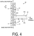
- FIG. 4 is an enlarged plan view illustrating the configuration of the electrode plate 20 according to the embodiment.
- the electrode plate 20 is substantially T-shaped and includes the body portion 21 extending in the layering direction D of the piezoelectric element 10 and the lead portion 22 extending in a direction intersecting the layering direction D.
- the body portion 21 of the electrode plate 20 includes a plurality of slits S.
- the slits S are notched so as to extend along a width direction of the body portion 21 (that is, a direction perpendicular to the layering direction D).
- the plurality of slits S are alternately notched from both side portions of the body portion 21, and are disposed side by side at substantially equal intervals along the layering direction D. All of the plurality of slits S have substantially the same length. Note that the length of the slits S refers to a length in a notched direction of the slits S (that is, the width direction of the body portion 21).
- the length of the plurality of slits S is set so that distal ends of the plurality of slits S overlap each other when viewed in the layering direction D.
- overlap means that adjacent ones of the slits S include regions facing each other when viewed in the layering direction D.
- the body portion 21 can be caused to expand and contract in the layering direction D by following the expansion and contraction of the piezoelectric element 10 in the layering direction D.
- peeling of the electrode plate 20 from the piezoelectric element 10 can be suppressed.
- the lead portion 22 of the electrode plate 20 includes a pair of side portions 22b and 22c.
- the side portion 22b is a side portion on a side of the distal end portion 10f(see FIG. 3 ) of the piezoelectric element 10 (see FIG. 3 )
- the side portion 22c is a side portion on a side of the base end portion 10e (see FIG. 3 ) of the piezoelectric element 10.
- the lead portion 22 includes, on at least one side portion (the side portion 22c in FIG. 4 ), recessed portions R recessed in the width direction of the lead portion 22.
- the width direction of the lead portion 22 is a direction perpendicular to a direction in which the lead portion 22 extends.
- the lead portion 22 twists with the recessed portions R as a starting point, and the lead portion 22 can be easily deformed. According to the embodiment, stress generated in a base end portion 22d of the lead portion 22 due to the expansion and contraction of the piezoelectric element 10 can be relaxed, and thus, peeling of the electrode plate 20 from the piezoelectric element 10 can be suppressed.
- a plurality of the recessed portions R may be disposed in one side portion of the lead portion 22.
- the lead portion 22 can be more easily deformed by following the expansion and contraction of the piezoelectric element 10 in the layering direction D.
- the stress generated in the base end portion 22d of the lead portion 22 due to the expansion and contraction of the piezoelectric element 10 can be further relaxed, and thus, peeling of the electrode plate 20 from the piezoelectric element 10 can be further suppressed.
- the number of the recessed portions R disposed in one side portion is not limited to two, and one recessed portion R may be disposed, or three or more of recessed portions R may be disposed.
- the plurality of recessed portions R provided in one side portion may all have substantially the same size, or may have different sizes.
- the recessed portion R may be disposed at least in the side portion 22c on the base end portion 10e side of the piezoelectric element 10, among the pair of side portions 22b and 22c of the lead portion 22.
- the side portion 22c on the base end portion 10e side to which a large tensile stress is applied when the piezoelectric element 10 is expanded can be easily deformed.
- stress generated in the base end portion 22d of the lead portion 22 when the piezoelectric element 10 expands can be relaxed, and thus, peeling of the electrode plate 20 from the piezoelectric element 10 can be suppressed.
- the recessed portion R may be disposed at a position closer to the base end portion 22d of the lead portion 22 than the distal end portion 22a (see FIG. 3 ) of the lead portion 22. As described above, by arranging the recessed portion R at a position close to the base end portion 22d adjacent to the body portion 21 where peeling occurs, the lead portion 22 can be easily deformed with respect to the expansion and contraction of the piezoelectric element 10.
- the stress generated in the base end portion 22d of the lead portion 22 due to the expansion and contraction of the piezoelectric element 10 can be further relaxed, and thus, peeling of the electrode plate 20 from the piezoelectric element 10 can be further suppressed.
- FIG. 5 is an enlarged plan view illustrating a shape of the recessed portion R located at the lead portion 22 according to the embodiment.
- the recessed portion R according to the embodiment may be substantially V-shaped.
- the lead portion 22 can be more easily deformed by following the expansion and contraction of the piezoelectric element 10 in the layering direction D.
- the stress generated in the base end portion 22d of the lead portion 22 due to the expansion and contraction of the piezoelectric element 10 can be further relaxed, and thus, peeling of the electrode plate 20 from the piezoelectric element 10 can be further suppressed.
- a bottom portion Ra of the recessed portion R may have a round shape.
- the piezoelectric actuator 1 can have improved reliability.
- the volume resistivity of the lead portion 22 increases, and thus, local heat generation may occur in the lead portion 22. That is, when the slits S extending over a long distance in the notch direction are disposed in the lead portion 22, the reliability of the piezoelectric actuator 1 may decrease.
- the recessed portion R having a small depth is disposed in the lead portion 22, so that local heat generation in the lead portion 22 can be suppressed, and therefore, excellent reliability of the piezoelectric actuator 1 can be maintained.
- the ratio of depth to width may be 2 times or less, for example.
- local heat generation in the lead portion 22 can be suppressed, and therefore, excellent reliability of the piezoelectric actuator 1 can be maintained.
- the depth of the recessed portion R may be one tenth or less of the width of the lead portion 22.
- the piezoelectric actuator 1 can be stably driven for a long period of time without hindering power supply from the lead terminal 30.
- the width of the recessed portion R may be, for example, in a range from 0.01 to 0.1 (mm), and the depth of the recessed portion R may be, for example, in a range from 0.05 to 1.0 (mm).
- FIG. 6 is an enlarged plan view illustrating an example of a configuration of the recessed portions R and a vicinity thereof in the lead portion 22 according to the embodiment.
- the side portion 22c where the recessed portions R are located at the lead portion 22 includes a first region 22c1 sandwiched between the pair of recessed portions R and second regions 22c2 other than the first region 22c1.
- the first region 22c1 and the second regions 22c2 may be substantially flush with each other in the vicinity of the pair of recessed portions R in the side portion 22c.
- FIGs. 7 to 9 are enlarged plan views illustrating other examples of the configuration of the recessed portions R and the vicinity thereof in the lead portion 22 according to the embodiment.
- the first region 22c1 may protrude outward with respect to the second regions 22c2 in the vicinity of the pair of recessed portions R in the side portion 22c.
- the first region 22c1 may be retracted inward with respect to the second regions 22c2 in the vicinity of the pair of recessed portions R in the side portion 22c.
- the first region 22c 1 may be retracted to the bottom portion Ra of the recessed portion R, so that the pair of recessed portions R are formed as one recessed portion R having a substantially trapezoidal shape, as illustrated in FIG. 9 .
- FIG. 10 is an enlarged perspective view illustrating another example of a configuration of the recessed portions R and a vicinity thereof in the lead portion 22 according to the embodiment.
- the plating film M for improving electric conductivity and/or thermal conductivity is disposed on the surface of the electrode plate 20 according to the embodiment, including the surface of the lead portion 22.
- sites where the plating film M is disposed are hatched with dots.
- the side portion 22c of the lead portion 22 may include a site where the plating film M is not formed in the first region 22c1 between adjacent ones of the recessed portions R.
- the first region 22c1 may be entirely a site where the plating film M is not formed.
- the lead portion 22 can be more easily deformed following the expansion and contraction of the piezoelectric element 10 in the layering direction D.
- peeling of the electrode plate 20 from the piezoelectric element 10 can be further suppressed.
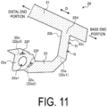
- FIG. 11 is an enlarged perspective view illustrating a configuration of the electrode plate 20 according to the embodiment. As illustrated in FIG. 11 , in the lead portion 22, the plurality of bent portions 22e are disposed in a region from the base end portion 22d to the distal end portion 22a.
- a bent portion 22e1 closest to the base end portion 22d is disposed along a corner portion located between adjacent side surfaces in the piezoelectric element 10 (see FIG. 3 ).
- the bent portion 22e2 located next to the bent portion 22e1 with respect to the base end portion 22d is located around the hole portion 22a1 in the distal end portion 22a and is a bent portion for making the distal end portion 22a substantially horizontal.
- a bent portion 22e3 located next to the bent portion 22e2 with respect to the base end portion 22d is located around the hole portion 22a1 in the distal end portion 22a, and is located so as to face the bent portion 22e2 via the hole portion 22a1.
- the recessed portions R located in the side portion 22c of the lead portion 22 may be disposed between the base end portion 22d and the bent portion 22e1.
- the recessed portions R are disposed at positions close to the base end portion 22d adjacent to the body portion 21 where peeling occurs. Therefore, among the stresses generated in the leads that changed in complex directions via the bent portion 22e1 following the expansion and contraction of the piezoelectric element 10 in the layering direction D, the stress on the base end portion 22d can be relaxed when the leads twist with the recessed portion R as a starting point. Thus, peeling of the electrode plate 20 from the piezoelectric element 10 can be further suppressed.
- the stress generated in the base end portion 22d of the lead portion 22 due to the expansion and contraction of the piezoelectric element 10 can be further relaxed, and thus, peeling of the electrode plate 20 from the piezoelectric element 10 can be further suppressed.
- the bent portions 22e2 and 22e3 located around the hole portion 22a1 may each include a through hole 22f.
- the piezoelectric actuator 1 can have improved reliability.
- the bonding material 31 may or may not enter the through hole 22f.
- FIGs. 12 to 14 Various variations of the embodiment will be described with reference to FIGs. 12 to 14 . Note that, in the various variations below, portions that are the same as those in the embodiment will be denoted by the same reference signs, and redundant explanations may be omitted.
- FIG. 12 is an enlarged plan view illustrating a configuration of the electrode plate 20 according to a first variation of the embodiment.
- the arrangement of the recessed portions R differs from the embodiment described above. Specifically, in the first variation, the recessed portions R are not disposed on the side portion 22c of the lead portion 22 on the base end portion 10e side (see FIG. 3 ) of the piezoelectric element 10 (see FIG. 3 ), but on the side portion 22b of the lead portion 22 on the distal end portion 10f side (see FIG. 3 ) of the piezoelectric element 10.
- the lead portion 22 can also be easily deformed by following the expansion and contraction of the piezoelectric element 10 in the layering direction D. Therefore, according to the first variation, peeling of the electrode plate 20 from the piezoelectric element 10 can be suppressed.
- FIG. 13 is an enlarged plan view illustrating a configuration of the electrode plate 20 according to a second variation of the embodiment.
- the lead portion 22 includes a plurality of the recessed portions R in each of the side portions 22b and 22c.
- the lead portion 22 easily twists with the recessed portions R in both of the side surfaces as starting points, and the lead portion 22 can be more easily deformed. Therefore, according to the second variation, peeling of the electrode plate 20 from the piezoelectric element 10 can be further suppressed.
- the recessed portions R located in each of the side portions 22b and 22c of the lead portion 22 may be located facing each other.
- the lead portion 22 is easily twisted in the region connecting the recessed portions R facing each other as a starting point.
- the lead portion 22 can be easily deformed in the vicinity of the recessed portions R even with a weak force.
- the recessed portions R facing each other in each of the side portions 22b and 22c may have substantially the same size or may have different sizes.
- FIG. 14 is an enlarged plan view illustrating a configuration of the electrode plate 20 according to a third variation of the embodiment.
- the lead portion 22 includes a plurality of the recessed portions R in each of the side portions 22b and 22c.
- the recessed portions R located in the side portion 22c of the piezoelectric element 10 on the base end portion 10e side are deeper than the recessed portions R located in the side portion 22b of the piezoelectric element 10 (see FIG. 3 ) on the distal end portion 10f side (see FIG. 3 ).
- the side portion 22c on the base end portion 10e side to which a large tensile stress is applied when the piezoelectric element 10 is expanded can be more easily deformed.
- stress generated in the base end portion 22d of the lead portion 22 when the piezoelectric element 10 expands can be further relaxed, and thus, peeling of the electrode plate 20 from the piezoelectric element 10 can be further suppressed.
- the piezoelectric actuator 1 includes the piezoelectric element 10 layered in a pillar shape, and the electrode plates 20 located at the side surfaces 10a and 10c of the piezoelectric element 10 and being electrically connected to the internal electrode layers 12 of the piezoelectric element 10.
- Each of the electrode plates 20 includes the body portion 21 extending in the layering direction D of the piezoelectric element 10 and the lead portion 22 extending in a direction intersecting the layering direction D and being electrically connected to the lead terminal 30.
- the lead portion 22 includes the recessed portion R recessed in the width direction of the lead portion 22 in at least one of the side portions 22c (22b).
- the recessed portion R is disposed at a position closer to the base end portion 22d of the lead portion 22 than the distal end portion 22a of the lead portion 22. Therefore, peeling of the electrode plate 20 from the piezoelectric element 10 can be further suppressed.
- the lead portion 22 includes the recessed portions R in each of the side portions 22b and 22c. Therefore, peeling of the electrode plate 20 from the piezoelectric element 10 can be further suppressed.
- the recessed portions R located in each of the side portions 22b and 22c of the lead portion 22 are located facing each other. Therefore, peeling of the electrode plate 20 from the piezoelectric element 10 can be further suppressed.
- the recessed portions R located in the side portion 22b of the piezoelectric element 10 on the base end portion 10e side are deeper than the recessed portions R located in the side portion 22c of the piezoelectric element 10 on the distal end portion 10f side. Therefore, peeling of the electrode plate 20 from the piezoelectric element 10 can be further suppressed.
- the recessed portion R is substantially V-shaped. Therefore, peeling of the electrode plate 20 from the piezoelectric element 10 can be further suppressed.
- the bottom portion Ra of the recessed portion R has a round shape.
- the piezoelectric actuator 1 can have improved reliability.
- the lead portion 22 includes the plurality of recessed portions R in the one side portion 22c (22b), and the one side portion 22c (22b) includes a site where the plating film M is not formed in a region (the first region 22c1) between adjacent ones of the recessed portions R. Therefore, peeling of the electrode plate 20 from the piezoelectric element 10 can be further suppressed.
- the lead portion 22 includes the plurality of bent portions 22e and the hole portion 22a1 through which the lead terminal 30 is inserted, and the bent portions 22e2 and 22e3 located around the hole portion 22a1 each include the through hole 22f.
- the piezoelectric actuator 1 can have improved reliability.
Landscapes
- General Electrical Machinery Utilizing Piezoelectricity, Electrostriction Or Magnetostriction (AREA)
Applications Claiming Priority (2)
| Application Number | Priority Date | Filing Date | Title |
|---|---|---|---|
| JP2020164695 | 2020-09-30 | ||
| PCT/JP2021/030169 WO2022070652A1 (ja) | 2020-09-30 | 2021-08-18 | 圧電アクチュエータ |
Publications (2)
| Publication Number | Publication Date |
|---|---|
| EP4224542A1 true EP4224542A1 (de) | 2023-08-09 |
| EP4224542A4 EP4224542A4 (de) | 2024-10-16 |
Family
ID=80949891
Family Applications (1)
| Application Number | Title | Priority Date | Filing Date |
|---|---|---|---|
| EP21874955.4A Pending EP4224542A4 (de) | 2020-09-30 | 2021-08-18 | Piezoelektrischer aktor |
Country Status (5)
| Country | Link |
|---|---|
| US (1) | US20230371390A1 (de) |
| EP (1) | EP4224542A4 (de) |
| JP (1) | JP7528239B2 (de) |
| CN (1) | CN116210370B (de) |
| WO (1) | WO2022070652A1 (de) |
Families Citing this family (1)
| Publication number | Priority date | Publication date | Assignee | Title |
|---|---|---|---|---|
| US12218610B1 (en) * | 2023-08-06 | 2025-02-04 | Cnpc Usa Corporation | Sensor system with an interior sensor and a piezoelectric power supply |
Family Cites Families (13)
| Publication number | Priority date | Publication date | Assignee | Title |
|---|---|---|---|---|
| JPH08242025A (ja) * | 1995-03-03 | 1996-09-17 | Hitachi Metals Ltd | 圧電アクチュエータ |
| JP2005183478A (ja) * | 2003-12-16 | 2005-07-07 | Ibiden Co Ltd | 積層型圧電素子 |
| JP4466321B2 (ja) * | 2004-10-28 | 2010-05-26 | Tdk株式会社 | 積層型圧電素子 |
| JP5135679B2 (ja) * | 2005-11-30 | 2013-02-06 | 株式会社村田製作所 | 積層型圧電素子の製造方法 |
| EP2259352B1 (de) * | 2008-04-11 | 2012-08-29 | Murata Manufacturing Co. Ltd. | Beschichteter piezoelektrischer aktuator |
| JP2010109057A (ja) * | 2008-10-29 | 2010-05-13 | Kyocera Corp | 積層型圧電素子およびこれを備えた噴射装置ならびに燃料噴射システム |
| JP5377100B2 (ja) | 2009-06-16 | 2013-12-25 | 京セラ株式会社 | 積層型圧電素子、これを用いた噴射装置および燃料噴射システム |
| CN102473834A (zh) * | 2009-07-28 | 2012-05-23 | 京瓷株式会社 | 层叠型压电元件及使用该层叠型压电元件的喷射装置以及燃料喷射系统 |
| WO2013114768A1 (ja) * | 2012-01-30 | 2013-08-08 | 京セラ株式会社 | 積層型圧電素子およびこれを備えた噴射装置ならびに燃料噴射システム |
| JPWO2013115341A1 (ja) * | 2012-01-31 | 2015-05-11 | 京セラ株式会社 | 積層型圧電素子およびこれを備えた噴射装置ならびに燃料噴射システム |
| JP2013211419A (ja) * | 2012-03-30 | 2013-10-10 | Kyocera Corp | 積層型圧電素子および圧電アクチュエータ |
| DE102013106223A1 (de) * | 2013-06-14 | 2014-12-18 | Epcos Ag | Vielschichtbauelement mit einer Außenkontaktierung, einer Weiterkontaktierung und einem Verbindungselement |
| JP2019102474A (ja) * | 2017-11-28 | 2019-06-24 | 京セラ株式会社 | 積層型圧電素子およびアクチュエータ |
-
2021
- 2021-08-18 WO PCT/JP2021/030169 patent/WO2022070652A1/ja not_active Ceased
- 2021-08-18 EP EP21874955.4A patent/EP4224542A4/de active Pending
- 2021-08-18 JP JP2022553535A patent/JP7528239B2/ja active Active
- 2021-08-18 CN CN202180064602.1A patent/CN116210370B/zh active Active
- 2021-08-18 US US18/029,281 patent/US20230371390A1/en active Pending
Also Published As
| Publication number | Publication date |
|---|---|
| JP7528239B2 (ja) | 2024-08-05 |
| CN116210370A (zh) | 2023-06-02 |
| EP4224542A4 (de) | 2024-10-16 |
| JPWO2022070652A1 (de) | 2022-04-07 |
| CN116210370B (zh) | 2026-04-21 |
| WO2022070652A1 (ja) | 2022-04-07 |
| US20230371390A1 (en) | 2023-11-16 |
Similar Documents
| Publication | Publication Date | Title |
|---|---|---|
| JPH09321363A (ja) | 圧電トランスおよびその支持構造 | |
| JP2606667B2 (ja) | 圧電磁器トランス及びその駆動方法 | |
| EP2610934B1 (de) | Piezoelektrischer aktuator | |
| EP4224542A1 (de) | Piezoelektrischer aktor | |
| JP2013211419A (ja) | 積層型圧電素子および圧電アクチュエータ | |
| JP7528240B2 (ja) | 圧電アクチュエータ | |
| US11944999B2 (en) | Vibration device and piezoelectric element | |
| US12389802B2 (en) | Piezoelectric actuator | |
| JP6809822B2 (ja) | 圧電アクチュエータ | |
| JP6144577B2 (ja) | 圧電アクチュエータ | |
| US20100308693A1 (en) | Piezoelectric Stack Actuator Assembly | |
| JPS61124183A (ja) | 積層型圧電体 | |
| JP5832338B2 (ja) | 圧電アクチュエータ | |
| EP1519425B1 (de) | Piezoelektrischer Aktor | |
| EP1519424A1 (de) | Piezoelektrischer Aktor | |
| JP2020017703A (ja) | 圧電アクチュエータ | |
| WO2025094830A1 (ja) | 圧電素子、圧電アクチュエータおよびマスフローコントローラ | |
| JP2536636B2 (ja) | 電歪効果素子組立体 | |
| WO2025094829A1 (ja) | 圧電素子、圧電アクチュエータおよびマスフローコントローラ | |
| WO2024080279A1 (ja) | 圧電素子 | |
| JPH04105374A (ja) | 圧電アクチュエータ | |
| WO2026063178A1 (ja) | 圧電アクチュエータおよびマスフローコントローラ | |
| JP2024058316A (ja) | 圧電素子 | |
| JPWO2013065710A1 (ja) | 圧電アクチュエータ | |
| CN112236876A (zh) | 压电致动器 |
Legal Events
| Date | Code | Title | Description |
|---|---|---|---|
| STAA | Information on the status of an ep patent application or granted ep patent |
Free format text: STATUS: THE INTERNATIONAL PUBLICATION HAS BEEN MADE |
|
| PUAI | Public reference made under article 153(3) epc to a published international application that has entered the european phase |
Free format text: ORIGINAL CODE: 0009012 |
|
| STAA | Information on the status of an ep patent application or granted ep patent |
Free format text: STATUS: REQUEST FOR EXAMINATION WAS MADE |
|
| 17P | Request for examination filed |
Effective date: 20230323 |
|
| AK | Designated contracting states |
Kind code of ref document: A1 Designated state(s): AL AT BE BG CH CY CZ DE DK EE ES FI FR GB GR HR HU IE IS IT LI LT LU LV MC MK MT NL NO PL PT RO RS SE SI SK SM TR |
|
| DAV | Request for validation of the european patent (deleted) | ||
| DAX | Request for extension of the european patent (deleted) | ||
| REG | Reference to a national code |
Ref country code: DE Ref legal event code: R079 Free format text: PREVIOUS MAIN CLASS: H01L0041047000 Ipc: H10N0030870000 |
|
| A4 | Supplementary search report drawn up and despatched |
Effective date: 20240916 |
|
| RIC1 | Information provided on ipc code assigned before grant |
Ipc: H10N 30/50 20230101ALI20240910BHEP Ipc: H10N 30/87 20230101AFI20240910BHEP |
|
| STAA | Information on the status of an ep patent application or granted ep patent |
Free format text: STATUS: EXAMINATION IS IN PROGRESS |
|
| 17Q | First examination report despatched |
Effective date: 20260311 |