EP4228012B1 - Wellenlängenabstimmbare leuchtdiode und verfahren zur herstellung derselben - Google Patents
Wellenlängenabstimmbare leuchtdiode und verfahren zur herstellung derselben Download PDFInfo
- Publication number
- EP4228012B1 EP4228012B1 EP22461577.3A EP22461577A EP4228012B1 EP 4228012 B1 EP4228012 B1 EP 4228012B1 EP 22461577 A EP22461577 A EP 22461577A EP 4228012 B1 EP4228012 B1 EP 4228012B1
- Authority
- EP
- European Patent Office
- Prior art keywords
- quantum well
- layer
- barrier layer
- active region
- fabricated
- Prior art date
- Legal status (The legal status is an assumption and is not a legal conclusion. Google has not performed a legal analysis and makes no representation as to the accuracy of the status listed.)
- Active
Links
Images


Classifications
-
- H—ELECTRICITY
- H10—SEMICONDUCTOR DEVICES; ELECTRIC SOLID-STATE DEVICES NOT OTHERWISE PROVIDED FOR
- H10H—INORGANIC LIGHT-EMITTING SEMICONDUCTOR DEVICES HAVING POTENTIAL BARRIERS
- H10H20/00—Individual inorganic light-emitting semiconductor devices having potential barriers, e.g. light-emitting diodes [LED]
- H10H20/80—Constructional details
- H10H20/81—Bodies
- H10H20/811—Bodies having quantum effect structures or superlattices, e.g. tunnel junctions
- H10H20/812—Bodies having quantum effect structures or superlattices, e.g. tunnel junctions within the light-emitting regions, e.g. having quantum confinement structures
-
- H—ELECTRICITY
- H10—SEMICONDUCTOR DEVICES; ELECTRIC SOLID-STATE DEVICES NOT OTHERWISE PROVIDED FOR
- H10H—INORGANIC LIGHT-EMITTING SEMICONDUCTOR DEVICES HAVING POTENTIAL BARRIERS
- H10H20/00—Individual inorganic light-emitting semiconductor devices having potential barriers, e.g. light-emitting diodes [LED]
- H10H20/01—Manufacture or treatment
- H10H20/011—Manufacture or treatment of bodies, e.g. forming semiconductor layers
- H10H20/013—Manufacture or treatment of bodies, e.g. forming semiconductor layers having light-emitting regions comprising only Group III-V materials
- H10H20/0137—Manufacture or treatment of bodies, e.g. forming semiconductor layers having light-emitting regions comprising only Group III-V materials the light-emitting regions comprising nitride materials
-
- H—ELECTRICITY
- H10—SEMICONDUCTOR DEVICES; ELECTRIC SOLID-STATE DEVICES NOT OTHERWISE PROVIDED FOR
- H10H—INORGANIC LIGHT-EMITTING SEMICONDUCTOR DEVICES HAVING POTENTIAL BARRIERS
- H10H20/00—Individual inorganic light-emitting semiconductor devices having potential barriers, e.g. light-emitting diodes [LED]
- H10H20/80—Constructional details
- H10H20/81—Bodies
- H10H20/8215—Bodies characterised by crystalline imperfections, e.g. dislocations; characterised by the distribution of dopants, e.g. delta-doping
-
- H—ELECTRICITY
- H10—SEMICONDUCTOR DEVICES; ELECTRIC SOLID-STATE DEVICES NOT OTHERWISE PROVIDED FOR
- H10H—INORGANIC LIGHT-EMITTING SEMICONDUCTOR DEVICES HAVING POTENTIAL BARRIERS
- H10H20/00—Individual inorganic light-emitting semiconductor devices having potential barriers, e.g. light-emitting diodes [LED]
- H10H20/80—Constructional details
- H10H20/81—Bodies
- H10H20/822—Materials of the light-emitting regions
- H10H20/824—Materials of the light-emitting regions comprising only Group III-V materials, e.g. GaP
- H10H20/825—Materials of the light-emitting regions comprising only Group III-V materials, e.g. GaP containing nitrogen, e.g. GaN
-
- H—ELECTRICITY
- H10—SEMICONDUCTOR DEVICES; ELECTRIC SOLID-STATE DEVICES NOT OTHERWISE PROVIDED FOR
- H10H—INORGANIC LIGHT-EMITTING SEMICONDUCTOR DEVICES HAVING POTENTIAL BARRIERS
- H10H20/00—Individual inorganic light-emitting semiconductor devices having potential barriers, e.g. light-emitting diodes [LED]
- H10H20/80—Constructional details
- H10H20/81—Bodies
- H10H20/816—Bodies having carrier transport control structures, e.g. highly-doped semiconductor layers or current-blocking structures
- H10H20/8162—Current-blocking structures
Definitions
- the present invention relates to a wavelength tunable light emitting diode and a method of fabrication of such diode.
- LEDs Conventional light emitting diodes
- the diode's undoped active region which contains one or more quantum wells, is located between p - and n -type doped layers.
- LEDs light emitting diodes
- GaN gallium nitride
- AlGaN alloys of gallium with aluminium
- InGaN indium
- Information about the structure of standard LEDs based on III group metal nitrides can be found, among others, in " Introduction to Nitride Semiconductor Blue Lasers and Light Emitting Diodes" by S.
- Devices wherein the colour of the emitted light can be changed within a broad range of the visible light spectrum are most often sets of independently controlled LEDs with strictly defined emission wavelengths.
- the most basic combination is made by blue ( ⁇ 450 nm), green ( ⁇ 520 nm) and red ( ⁇ 650 nm) colour diodes.
- blue ( ⁇ 450 nm) green ( ⁇ 520 nm) and red ( ⁇ 650 nm) colour diodes.
- the level of LED integration can occur at various stages of the engineering process. These can be large LEDs present in the RGB LED strips available on the market or micro-LED arrays. Methods of integration of single micro-LEDs for the purpose of production of multi-colour displays are disclosed in the review publication titled " Full-Color Realization of Micro-LED Displays" by Y.
- Monolithic displays containing diodes with all three primary colours can be made only within the III nitrides, because the band gap of the indium gallium nitride (InGaN) alloy is the only one to cover the whole visible spectrum.
- the emission wavelength increases in line with the increase in the indium content in the InGaN alloy and in order to achieve the red light emission the indium content in the quantum well alloy should be circa 40%.
- Such a high indium content in planar structures is difficult to obtain due to high stresses of the InGaN layers and to the demanding conditions for epitaxy. Integration of indium in the micro-LED structure can be controlled at the nanostructure level, which is disclosed in the publication by Ra, Y.-H. et al.
- the emission wavelength was changed continuously from 690 nm (for 3 V) to 500 nm (for 10 V). This effect was explained by an appropriate model of electric field distribution in the nanorod structure.
- current with a low density flows preferably through InGaN wells with a high indium content on the top of the nanorods.
- current with an increasingly higher density flows successively through the quantum wells on the slants and the side walls of the nanorods.
- the carrier injection effectiveness reaches the maximum successively for multi-quantum wells with the 25% indium content and green electroluminescence and then with the 15% indium content and blue electroluminescence.
- electrically tunable electroluminescence ranging from 460 nm to 650 nm was obtained.
- red, green and blue light emissions are still achieved from InGaN wells with varied indium contents.
- a diode according to the invention which has an epitaxial layer structure built of nitrides of group III metals applied to a crystalline substrate.
- This structure is composed, counted from the crystalline substrate, of at least an n -type conductivity layer, a light emitting active region with one quantum well, and a p -type conductivity layer.
- the present invention consists in the active region that is composed, counted from the crystalline substrate, of a lower n -type doped barrier layer, a lower n -type doped part of the quantum well, an upper p -type doped part of the quantum well, and an upper p -type doped barrier layer.
- each part of the quantum well ranges from 4 nm to 25 nm.
- the doping level of each part of the quantum well ranges from 1 ⁇ 10 19 cm -3 to 2 ⁇ 10 20 cm -3 , while the doping level of the barrier layer is up to 25% of the doping level of the part of the quantum well that is adjacent to said barrier layer.
- each part of the quantum well is made of the In x Ga 1-x N indium gallium nitride alloy
- each barrier layer is made of the In y Ga 1-y N indium gallium nitride alloy, wherein the indium content in said alloys is determined by the following correlation: 0 ⁇ y ⁇ x ⁇ 0.3.
- the width of the upper part of the quantum well is between 20% and 80% of the sum of widths of both parts of the quantum well.
- an electron blocking layer made of the Al x Ga 1-x N aluminium gallium nitride alloy wherein the aluminium content ranges from 0 to 0.2, wherein the doping level of said layer ranges from 5x 10 18 cm -3 to 5 ⁇ 10 19 cm -3 .
- the method according to the invention consists in fabricating an epitaxial layer structure on a crystalline substrate, with the structure's containing, counted from the crystalline substrate, at least an n -type conductivity layer, a light emitting active region with one quantum well and a p -type conductivity layer, of nitrides of group III metals in the process of nitrogen plasma assisted molecular beam epitaxy (PAMBE) growth.
- PAMBE nitrogen plasma assisted molecular beam epitaxy
- the invention is characterised in that an n -type conductivity layer, a four-layer active region and a p -type conductivity layer are successively fabricated on a crystalline substrate. While fabricating the active region, first its lower n -type doped barrier layer is fabricated.
- a lower n -type doped part of the quantum well is fabricated, after which an upper p -type doped part of the quantum well is fabricated.
- the fabrication of the active region is finished by applying an upper p -type doped barrier layer. While fabricating both parts of the quantum well, their width ranging from 4 nm to 25 nm and the doping level ranging from 1 ⁇ 10 19 cm -3 to 2 ⁇ 10 20 cm -3 are applied. While fabricating each barrier layer of the active region, the doping level of up to 25% of the doping level of the part of the quantum well that is adjacent to the barrier layer being fabricated is applied.
- each part of the quantum well is made of the In x Ga 1-x N indium gallium nitride alloy
- each barrier layer is made of the In y Ga 1-y N indium gallium nitride alloy, by applying the indium content in said alloys that is determined by the following correlation: 0 ⁇ y ⁇ x ⁇ 0.3.
- an upper part of the quantum well is fabricated with the width being between 20% and 80% of the sum of widths of both parts of the quantum well.
- an electron blocking layer is applied additionally between the upper barrier layer and the p-type conductivity layer.
- the Al x Ga 1-x N aluminium gallium nitride alloy is used, wherein the aluminium content ranges from 0 to 0.2 and the doping level ranges from 5 ⁇ 10 18 cm -3 to 5 ⁇ 10 19 cm -3 .
- the epitaxial growth of the layer structure is performed in metal-rich conditions.
- Epitaxial layers of said structure are applied at the temperature ranging from 600°C to 800°C, while nitrogen for epitaxial growth of the layer structure is supplied in the form of plasma excited by a power supply unit generating a power between 100 and 600 W, with the nitrogen flow between 1 and 15 cm 3 per minute.
- the invention breaks the conviction prevailing commonly among specialists that in order to obtain red electroluminescence of a LED fabricated using the technology of nitrides of group III metals, the indium content in the quantum well must be increased to circa 35%. It has turned out unexpectedly that it is possible to obtain lighting from a single quantum well placed in the layer structure of a LED with a much higher wavelength than could be expected from the energy of the band gap of the alloy forming the quantum well, and that the wavelength of emission from such a quantum well can be changed continuously by changing the density of the current flowing through the LED structure. This is possible through an appropriate engineering of the doping of the active region containing one quantum well with the width between 8 nm and 50 nm.
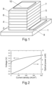
- Fig.1 presents a schematic axonometric view of the diode according to the invention.
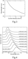
- Fig.2 presents the light-current-voltage (LIV) characteristics of an embodiment of a diode according to the invention, while Fig.3 presents the correlation between the emission wavelength and the density of the current powering said diode.
- Fig.4 presents standardised spectra of electroluminescence of the same diode for various current densities ranging from 0.5 A/cm 2 to 200 A/cm 2
- Fig.5 presents points corresponding to said spectra in a chromaticity diagram according to the CIE 1931 standard.
- Fig.6 presents an example time diagram of control of the power supply of the diode according to the invention.
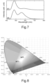
- Fig.7 presents spectra of white light obtained by mixing blue and yellow light by the method according to the diagram in Fig.6
- Fig.8 presents points corresponding to said spectra in a chromaticity diagram according to the CIE 1931 standard.
- Fig.9 presents diagrams of the band structures of the active region, which reflect the scheme of operation of a diode according to the invention for four different voltages powering said diode.
- Fig.1 shows that the embodiment of a diode according to the invention contains a set of epitaxial layers, which is composed successively, counted from the crystalline substrate 1, of an n -type conductivity layer 2, an active region (layers from 3 through 6), an electron blocking layer 7 and a p -type conductivity layer 8.
- the aforementioned active region is composed of four successive layers: a lower n -type doped barrier layer 3, a lower n -type doped part 4 of the quantum well, an upper p -type doped part 5 of the quantum well, and an upper p -type doped barrier layer 6.
- Such a diode contains a first current terminal 9, connected electrically with the lower n -type conductivity layer 2, and a second current terminal 10, connected electrically with the p -type conductivity layer 8.
- This diode was fabricated in the process of nitrogen plasma assisted molecular beam epitaxy (PAMBE) growth in a Veeco GEN-20 reactor.
- the substrate 1 with the thickness of 350 ⁇ m, made of gallium nitride, was heated in a prechamber of said reactor at the temperature of 150°C for 90 minutes. The heating of the substrate 1 was continued for 30 minutes in a preparatory chamber at the temperature of 650°C. The heated substrate 1 was transferred to a growth chamber.
- the layer epitaxy was performed in metal-rich conditions. Nitrogen in the form of plasma excited by radio frequencies by a power supply unit was used for the growth, wherein the plasma parameters varied depending on the currently grown layer.
- Metals forming the alloys such as gallium, indium and aluminium, and n -type dopant materials, that is, silicon and germanium, were evaporated from standard Knudsen cells, while as a source of p -type magnesium dopant a special structure of the Knudsen cell was used, which had an additional valve inside the cell, which valve allows a faster adjustment of the magnesium dopant atom flux size during the growth.
- the purity of the elements used for the epitaxy exceeded 99.999%.
- a layer 2 ( n -type) with the thickness of 100 nm was fabricated of GaN, with the silicon doping level of 1 ⁇ 10 18 cm -3 .
- an active region (3, 4, 5, 6) was fabricated, which at the bottom contained a lower barrier layer 3 with the thickness of 60 nm, made of the silicon-doped In 0.02 Ga 0.98 N alloy with the doping level of 4 ⁇ 10 18 cm -3 .
- Another layer of said region was a lower part of the quantum well 4 with the thickness of 7.8 nm, made of the germanium-doped In 0.17 Ga 0.83 N alloy with the doping level of 6 ⁇ 10 19 cm -3 .
- the next layer of the active region was an upper part of the quantum well 5 with the thickness of 7.8 nm, made of the magnesium-doped In 0.17 Ga 0.83 N alloy with the doping level of 6 ⁇ 10 19 cm -3 .
- the last layer of the active region was an upper barrier layer 6 with the thickness of 60 nm, made of the magnesium-doped In 0.02 Ga 0.98 N alloy with the doping level of 4 ⁇ 10 18 cm -3 .
- an electron blocking layer 7 with the thickness of 20 nm, made of magnesium-doped GaN with the doping level of 2 ⁇ 10 19 cm -3 , was fabricated.
- a p-type conductivity layer 8 was fabricated, composed of a first sublayer with the thickness of 100 nm, made of magnesium-doped gallium nitride with the doping level of 1 ⁇ 10 18 cm -3 , of a second sublayer with the thickness of 40 nm, made of the magnesium-doped In 0.02 Ga 0.98 N alloy with the doping level of 6 ⁇ 10 19 cm -3 , and of a third sublayer with the thickness of 5 nm, made of the magnesium-doped In 0.17 Ga 0.83 N alloy with the doping level of 2 ⁇ 10 20 cm -3 .
- metallisation composed of a sequence of Ni/Au with the thickness of 2.5/7.5 nm was applied and subjected to the heating process in the nitrogen and oxygen atmosphere for one minute at the temperature of 500°C. Subsequently, said structure was subjected to photolithography and reactive ion etching to form mesas with the dimensions of 350 ⁇ 350 ⁇ m and 100 ⁇ 100 ⁇ m, which were etched 400 nm deep, that is, to the level of the n -type conductivity layer 2.
- Ni/Au/Pt metallisation with the thickness of 25/75/60 nm was applied in the form of grids with the dimensions of 340 ⁇ 340 ⁇ m on the mesas with the dimensions of 350 ⁇ 350 ⁇ m and in the form of solid squares with the dimensions of 90 ⁇ 90 ⁇ m on the mesas with the dimensions of 100 ⁇ 100 ⁇ m, composing the second (upper) current terminal 10.
- the metallisations were heated again in the nitrogen and oxygen atmosphere for ten minutes at the temperature of 500°C.
- metallisation of Ti/Al/Ni/ Au with the thickness of 30/60/40/75 nm, composing the first (lower) current terminal 9 was applied on the side of the mesas.
- the electrooptical properties of the fabricated structure were measured by the needle method, wherein a power supply unit and a voltage meter were interfaced with a spectrometer and an optical power meter.
- the optical power meter was placed at a constant height above the sample surface but it did not collect the whole light emitted from the sample to the outside, hence the optical powers presented in the chart ( Fig.2 ) are purely qualitative.
- the embodiment of a diode with the mesa size of 350 ⁇ 350 ⁇ m has current-voltage (I-V) characteristics in the forward direction that is typical of a LED, but the diode opening voltage is relatively low: circa 2.2 V.
- Optical power emitted from said diode increases approximately in a linear manner as a function of current density.
- Fig.3 presents a semi-log plot with the change in the wavelength of the light emitted from the embodiment of a diode as a function of current density. The spectrum maximum shifts towards the shorter waves within the range from 645 nm to 481 nm in line with the increase in the density of the current flowing through the diode within the range from 0.3 A/cm 2 to 400 A/cm 2 .
- Fig.4 presents standardised electroluminescence spectra for nine selected current densities, designated with letters from (a) through (i) in the drawing.
- Fig.5 the same spectra (for the same current densities as in Fig.4 ) are presented in the chromaticity diagram of the CIE1931 colour space.
- the colour of the light emitted from the diode according to the invention can be continuously changed within the whole visible spectrum, that is, from the red, to orange, yellow, green, cyan to blue, by changing the density of the current flowing through the diode, which is equivalent to a change in the voltage powering the diode.
- Fig.6 A scheme of such a power supply is presented in Fig.6 .
- the current (I) or voltage (V) powering the diode changes stepwise.
- a power supply level By selecting a power supply level, the wavelength of one of the peaks in the final spectrum is changed, and its intensity is adjusted by the duration.
- This way it is possible to set, for example, four power supply levels, with three responsible for emission of light of an appropriate primary colour: blue I 1 (V 1 ), green I 2 (V 2 ) and red I 3 (V 3 ), and the zero level I 0 (V 0 ), for which no emission occurs.
- the final lighting power can be reduced by prolonging the duration of the zero level.
- Fig.7 presents two spectra (A) and (B) of white light, obtained with the use of the power supply scheme described above, which uses two different power supply levels (V 1 and V 2 ) for the embodiment of a diode according to the invention with the dimensions of 100 ⁇ 100 ⁇ m.
- Fig.8 the same spectra as in Fig.7 are presented in the chromaticity diagram of the CIE 1931 colour space.
- Such a waveform of the power supply was achieved with the use of a programmable arbitrary power supply unit, Siglent SDG2042X.
- Fig.9 presents four band diagrams as a function of distance from crystalline substrate, prepared for four different voltages applied to the diode according to the invention, which illustrate the method of operation of such a diode.
- Diagram a) refers to the voltage of 2 V
- conduction and valence bands inside quantum wells are bent because of the strong doping of the individual parts of quantum wells.
- the energy difference between the energy levels of the wave functions for holes and electrons changes in line with the increase in the voltage powering the diode from 2.2 eV to 2.6 eV. This effect is responsible for the change in the colour of the emission from the diode.
- Diagrams c) and d) prepared for higher voltages that is, 3 V and 3.5 V, respectively, show that a quantum well is then virtually flat and resembles a case of an undoped well, wherein the energy difference between the energy levels of the wave functions for holes and electrons does not change and the electroluminescence wavelength is defined by the indium content in the quantum well.
Landscapes
- Led Devices (AREA)
- Physical Deposition Of Substances That Are Components Of Semiconductor Devices (AREA)
Claims (9)
- Lichtemittierende Diode mit einer variablen Lichtemissionsfarbe, die eine epitaktische Schichtstruktur aufweist, die aus Nitriden von Metallen der Gruppe III aufgebaut ist, die auf ein kristallines Substrat aufgebracht sind, wobei die Struktur, vom kristallinen Substrat aus gerechnet, aus mindestens einer n-Typ-Leitfähigkeitsschicht, einem lichtemittierenden aktiven Bereich mit einem Quantentopf und einer p-Typ-Leitfähigkeitsschicht zusammengesetzt ist, dadurch gekennzeichnet, dass der aktive Bereich (3, 4, 5, 6), vom kristallinen Substrat (1) aus gerechnet, aus einer unteren n-Typ-dotierten Sperrschicht (3), einem unteren n-dotierten Teil (4) des Quantentopfs, einem oberen p-dotierten Teil (5) des Quantentopfs und einer oberen p-dotierten Sperrschicht (6) besteht, wobei die Breite jedes Teils (4, 5) des Quantentopfs im Bereich von 4 nm bis 25 nm liegt, das Dotierungsniveau jedes Teils (4, 5) des Quantentopfes im Bereich von 1 × 1019 cm-3 bis 2 × 1020 cm-3 liegt, während das Dotierungsniveau der Sperrschicht (3, 6) bis zu 25% des Dotierungsniveaus des Teils des Quantentopfes (4, 5) beträgt, der an die Sperrschicht (3, 6) angrenzt.
- Die Diode nach Anspruch 1, dadurch gekennzeichnet, dass jeder Teil (4, 5) des Quantentopfes aus der Indium-Gallium-Nitrid-Legierung InxGa1-xN hergestellt ist, jede Sperrschicht (3, 6) aus der Indium-Gallium-Nitrid-Legierung InyGa1-yN hergestellt ist, wobei der Indiumgehalt in den Legierungen durch die folgende Korrelation bestimmt ist: 0≤y <X≤0,3.
- Die Diode nach Anspruch 1 oder 2, dadurch gekennzeichnet, dass die Breite des oberen Teils (5) des Quantentopfes zwischen 20% und 80% der Summe der Breiten der beiden Teile (4, 5) des Quantentopfes beträgt.
- Die Diode nach Anspruch 1 oder 2 oder 3, dadurch gekennzeichnet, dass sich zwischen der oberen Sperrschicht (6) und der p-Leitfähigkeitsschicht (8) zusätzlich eine Elektronensperrschicht (7) aus der Aluminium-Galliumnitrid-Legierung AlxGa1-xN befindet, wobei der Aluminiumgehalt zwischen 0 und 0,2 liegt, wobei das Dotierungsniveau der Schicht (7) zwischen 5 × 1018 cm-3 to 5 × 1019 cm-3 liegt.
- Ein Verfahren zur Herstellung einer lichtemittierenden Diode mit einer variablen Lichtemissionsfarbe, das darin besteht, eine epitaktische Schichtstruktur auf einem kristallinen Substrat herzustellen, wobei die Struktur, vom kristallinen Substrat aus gerechnet, mindestens eine n-Typ-Leitfähigkeitsschicht, einen lichtemittierenden aktiven Bereich mit einem Quantentopf und eine p-Typ-Leitfähigkeitsschicht enthält, von Nitriden aus Metallen der Gruppe III im Verfahren des Stickstoff Plasma-unterstützten Molekularstrahl-Epitaxie (PAMBE)-Wachstums, dadurch gekennzeichnet, dass eine n-Typ-Leitfähigkeitsschicht (2), ein vierschichtiger aktiver Bereich (3, 4, 5, 6) und eine p-Typ-Leitfähigkeitsschicht (8) nacheinander auf einem kristallinen Substrat (1) hergestellt werden, wobei bei der Herstellung des aktiven Bereichs (3, 4, 5, 6) zunächst seine untere n-dotierte Barriereschicht (3) hergestellt wird, anschließend ein unterer n-dotierter Teil (4) des Quantentopfs hergestellt wird, danach ein oberer p-dotierter Teil (5) des Quantentopfs hergestellt wird und schließlich eine obere p-dotierte Barriereschicht (6) hergestellt wird, wobei bei der Herstellung jedes Teils (4, 5) des Quantentopfs, ihre Breite im Bereich von 4 nm bis 25 nm und das Dotierungsniveau im Bereich von 1 × 1019 cm-3 to 2 × 1020 cm-3 angewandt werden, und während der Herstellung jeder Barriereschicht (3, 6) des aktiven Bereichs das Dotierungsniveau von bis zu 25% des Dotierungsniveaus des Teils (4, 5) des Quantentopfs, der an die herzustellende Barriereschicht (3, 6) angrenzt, angewandt wird.
- Das Verfahren nach Anspruch 5, dadurch gekennzeichnet, dass jeder Teil (4, 5) des Quantentopfes aus der Indium-Gallium-Nitrid-Legierung InxGa1-xN hergestellt ist, und jede Sperrschicht (3, 6) aus der Indium-Gallium-Nitrid-Legierung InyGa1-yN hergestellt ist, durch Anwendung des Indiumgehalts in diesen Legierungen, der durch die folgende Korrelation bestimmt wird: 0≤y<x≤0,3.
- Das Verfahren nach Anspruch 5 oder 6, dadurch gekennzeichnet, dass beim Wachstumsprozess des aktiven Bereichs (3, 4, 5, 6) ein oberer Teil (5) des Quantentopfs mit einer Breite zwischen 20% und 80% der Summe der Breiten der beiden Teile (4, 5) des Quantentopfs hergestellt wird.
- Das Verfahren nach Anspruch 5 oder 6 oder 7, dadurch gekennzeichnet, dass zwischen der oberen Barriereschicht (6) und der p-Typ-Leitfähigkeitsschicht (8) zusätzlich eine Elektronensperrschicht (7) aufgebracht wird und für die Herstellung dieser Schicht die Aluminium-Gallium-Nitrid-Legierung AlxGa1-xN verwendet wird, wobei der Aluminiumgehalt im Bereich von 0 bis 0,2 liegt und das Dotierungsniveau der Schicht (7) im Bereich von 5×1018 cm-3 to 5x 1019cm-3 liegt.
- Das Verfahren nach Anspruch 5 oder 6 oder 7 oder 8, dadurch gekennzeichnet, dass das epitaktische Wachstum der Schichtstruktur unter metallreichen Bedingungen durchgeführt wird, die epitaktischen Schichten (2 bis 8) bei einer Temperatur im Bereich von 600°C bis 800°C aufgebracht werden, während Stickstoff für das epitaktische Wachstum der Schichtstruktur in Form eines Plasmas zugeführt wird, das durch eine Stromversorgungseinheit angeregt wird, die eine Leistung zwischen 100 und 600 W erzeugt, wobei der Stickstofffluss zwischen 1 und 15 cm3 pro Minute liegt.
Applications Claiming Priority (1)
| Application Number | Priority Date | Filing Date | Title |
|---|---|---|---|
| PL440375A PL440375A1 (pl) | 2022-02-12 | 2022-02-12 | Dioda elektroluminescencyjna o zmiennej barwie emisji i sposób wytwarzania takiej diody |
Publications (3)
| Publication Number | Publication Date |
|---|---|
| EP4228012A1 EP4228012A1 (de) | 2023-08-16 |
| EP4228012C0 EP4228012C0 (de) | 2024-09-25 |
| EP4228012B1 true EP4228012B1 (de) | 2024-09-25 |
Family
ID=83006096
Family Applications (1)
| Application Number | Title | Priority Date | Filing Date |
|---|---|---|---|
| EP22461577.3A Active EP4228012B1 (de) | 2022-02-12 | 2022-06-23 | Wellenlängenabstimmbare leuchtdiode und verfahren zur herstellung derselben |
Country Status (2)
| Country | Link |
|---|---|
| EP (1) | EP4228012B1 (de) |
| PL (2) | PL440375A1 (de) |
Families Citing this family (1)
| Publication number | Priority date | Publication date | Assignee | Title |
|---|---|---|---|---|
| CN117457821B (zh) * | 2023-12-21 | 2024-03-08 | 江西兆驰半导体有限公司 | Micro-LED外延片及其制备方法、Micro-LED |
Family Cites Families (3)
| Publication number | Priority date | Publication date | Assignee | Title |
|---|---|---|---|---|
| JP4027609B2 (ja) * | 2001-02-13 | 2007-12-26 | 独立行政法人科学技術振興機構 | 発光ダイオードの発光色制御方法 |
| KR20090086942A (ko) * | 2006-09-08 | 2009-08-14 | 에이전시 포 사이언스, 테크놀로지 앤드 리서치 | 가변 파장 발광 다이오드 |
| JP2018516466A (ja) | 2015-06-05 | 2018-06-21 | オステンド・テクノロジーズ・インコーポレーテッド | 多重活性層へのキャリア注入を選定した発光構造 |
-
2022
- 2022-02-12 PL PL440375A patent/PL440375A1/pl unknown
- 2022-06-23 EP EP22461577.3A patent/EP4228012B1/de active Active
- 2022-06-23 PL PL22461577.3T patent/PL4228012T3/pl unknown
Also Published As
| Publication number | Publication date |
|---|---|
| EP4228012C0 (de) | 2024-09-25 |
| PL440375A1 (pl) | 2023-08-14 |
| EP4228012A1 (de) | 2023-08-16 |
| PL4228012T3 (pl) | 2025-01-27 |
Similar Documents
| Publication | Publication Date | Title |
|---|---|---|
| US6329676B1 (en) | Flat panel solid state light source | |
| CN107851968B (zh) | 具有到多个有源层中的选择性载流子注入的发光结构 | |
| EP2254164B1 (de) | Lichtemittierendes verbundhalbleiterbauelement und beleuchtungsvorrichtung damit sowie verfahren zur herstellung des lichtemittierenden verbundhalbleiterbauelements | |
| US7348600B2 (en) | Nitride semiconductor device, and its fabrication process | |
| US8022388B2 (en) | Broadband light emitting device lamps for providing white light output | |
| CN106165125B (zh) | 发光二极管及其制备方法 | |
| EP2200100A1 (de) | Lichtemittierendes iii-nitrid-halbleiterbauelement | |
| KR101611412B1 (ko) | 발광 소자 | |
| JP2003520453A (ja) | チャーピングされた多層井戸活性領域led | |
| KR101460387B1 (ko) | 발광 구조물 | |
| US11393948B2 (en) | Group III nitride LED structures with improved electrical performance | |
| Lu et al. | Phosphor-free monolithic white-light LED | |
| EP4228012A1 (de) | Wellenlängenabstimmbare leuchtdiode und verfahren zur herstellung derselben | |
| CN114078989B (zh) | 全彩发光器件 | |
| EP4340050A1 (de) | Mehrband-leuchtdiode | |
| KR20080068244A (ko) | 표면 플라즈몬을 이용하는 발광 다이오드 | |
| KR100972978B1 (ko) | 질화물 반도체 소자 | |
| US20260052802A1 (en) | Growth engineering of monolithic color-tunable light emitting diodes and methods thereof | |
| US20260052803A1 (en) | Growth engineering of monolithic and at least red emitting color-tunable light emitting diodes and methods thereof | |
| CN102709418A (zh) | 一种光谱可调的ZnO/GaN基白光发光器件结构 | |
| Dussaigne et al. | Monolithic white light emitting diodes with a broad emission spectrum | |
| HK40075839A (en) | Light emitting structures with selective carrier injection into multiple active layers | |
| US20010007361A1 (en) | Semiconductor light emitting device with high yield and low power consumption | |
| CN120584409A (zh) | 半导体器件单片阵列、模板晶片、制造模板晶片的方法、制造半导体器件阵列的方法 | |
| JP2005353651A (ja) | 半導体発光素子およびその製造方法 |
Legal Events
| Date | Code | Title | Description |
|---|---|---|---|
| STAA | Information on the status of an ep patent application or granted ep patent |
Free format text: STATUS: UNKNOWN |
|
| PUAI | Public reference made under article 153(3) epc to a published international application that has entered the european phase |
Free format text: ORIGINAL CODE: 0009012 |
|
| STAA | Information on the status of an ep patent application or granted ep patent |
Free format text: STATUS: THE APPLICATION HAS BEEN PUBLISHED |
|
| AK | Designated contracting states |
Kind code of ref document: A1 Designated state(s): AL AT BE BG CH CY CZ DE DK EE ES FI FR GB GR HR HU IE IS IT LI LT LU LV MC MK MT NL NO PL PT RO RS SE SI SK SM TR |
|
| RIN1 | Information on inventor provided before grant (corrected) |
Inventor name: SKIERBISZEWSKI, CZESLAW Inventor name: WOLNY, PAWEL Inventor name: HAJDEL, MATEUSZ Inventor name: MUZIOL, GRZEGORZ Inventor name: NOWAKOWSKI-SZKUDLAREK, KRZESIMIR Inventor name: CHLIPALA, MIKOLAJ Inventor name: TURSKI, HENRYK Inventor name: ZAK, MIKOLAJ |
|
| STAA | Information on the status of an ep patent application or granted ep patent |
Free format text: STATUS: REQUEST FOR EXAMINATION WAS MADE |
|
| 17P | Request for examination filed |
Effective date: 20231205 |
|
| RBV | Designated contracting states (corrected) |
Designated state(s): AL AT BE BG CH CY CZ DE DK EE ES FI FR GB GR HR HU IE IS IT LI LT LU LV MC MK MT NL NO PL PT RO RS SE SI SK SM TR |
|
| GRAP | Despatch of communication of intention to grant a patent |
Free format text: ORIGINAL CODE: EPIDOSNIGR1 |
|
| STAA | Information on the status of an ep patent application or granted ep patent |
Free format text: STATUS: GRANT OF PATENT IS INTENDED |
|
| RIC1 | Information provided on ipc code assigned before grant |
Ipc: H01L 33/14 20100101ALN20240530BHEP Ipc: H01L 33/32 20100101ALI20240530BHEP Ipc: H01L 33/06 20100101ALI20240530BHEP Ipc: H01L 33/02 20100101ALI20240530BHEP Ipc: H01L 33/00 20100101AFI20240530BHEP |
|
| INTG | Intention to grant announced |
Effective date: 20240620 |
|
| GRAS | Grant fee paid |
Free format text: ORIGINAL CODE: EPIDOSNIGR3 |
|
| GRAA | (expected) grant |
Free format text: ORIGINAL CODE: 0009210 |
|
| STAA | Information on the status of an ep patent application or granted ep patent |
Free format text: STATUS: THE PATENT HAS BEEN GRANTED |
|
| AK | Designated contracting states |
Kind code of ref document: B1 Designated state(s): AL AT BE BG CH CY CZ DE DK EE ES FI FR GB GR HR HU IE IS IT LI LT LU LV MC MK MT NL NO PL PT RO RS SE SI SK SM TR |
|
| REG | Reference to a national code |
Ref country code: GB Ref legal event code: FG4D |
|
| REG | Reference to a national code |
Ref country code: CH Ref legal event code: EP |
|
| REG | Reference to a national code |
Ref country code: DE Ref legal event code: R096 Ref document number: 602022006392 Country of ref document: DE |
|
| REG | Reference to a national code |
Ref country code: IE Ref legal event code: FG4D |
|
| U01 | Request for unitary effect filed |
Effective date: 20241015 |
|
| U07 | Unitary effect registered |
Designated state(s): AT BE BG DE DK EE FI FR IT LT LU LV MT NL PT RO SE SI Effective date: 20241031 |
|
| PG25 | Lapsed in a contracting state [announced via postgrant information from national office to epo] |
Ref country code: NO Free format text: LAPSE BECAUSE OF FAILURE TO SUBMIT A TRANSLATION OF THE DESCRIPTION OR TO PAY THE FEE WITHIN THE PRESCRIBED TIME-LIMIT Effective date: 20241225 |
|
| PG25 | Lapsed in a contracting state [announced via postgrant information from national office to epo] |
Ref country code: GR Free format text: LAPSE BECAUSE OF FAILURE TO SUBMIT A TRANSLATION OF THE DESCRIPTION OR TO PAY THE FEE WITHIN THE PRESCRIBED TIME-LIMIT Effective date: 20241226 |
|
| PG25 | Lapsed in a contracting state [announced via postgrant information from national office to epo] |
Ref country code: RS Free format text: LAPSE BECAUSE OF FAILURE TO SUBMIT A TRANSLATION OF THE DESCRIPTION OR TO PAY THE FEE WITHIN THE PRESCRIBED TIME-LIMIT Effective date: 20241225 |
|
| PG25 | Lapsed in a contracting state [announced via postgrant information from national office to epo] |
Ref country code: RS Free format text: LAPSE BECAUSE OF FAILURE TO SUBMIT A TRANSLATION OF THE DESCRIPTION OR TO PAY THE FEE WITHIN THE PRESCRIBED TIME-LIMIT Effective date: 20241225 Ref country code: NO Free format text: LAPSE BECAUSE OF FAILURE TO SUBMIT A TRANSLATION OF THE DESCRIPTION OR TO PAY THE FEE WITHIN THE PRESCRIBED TIME-LIMIT Effective date: 20241225 Ref country code: GR Free format text: LAPSE BECAUSE OF FAILURE TO SUBMIT A TRANSLATION OF THE DESCRIPTION OR TO PAY THE FEE WITHIN THE PRESCRIBED TIME-LIMIT Effective date: 20241226 |
|
| PG25 | Lapsed in a contracting state [announced via postgrant information from national office to epo] |
Ref country code: IS Free format text: LAPSE BECAUSE OF FAILURE TO SUBMIT A TRANSLATION OF THE DESCRIPTION OR TO PAY THE FEE WITHIN THE PRESCRIBED TIME-LIMIT Effective date: 20250125 |
|
| PG25 | Lapsed in a contracting state [announced via postgrant information from national office to epo] |
Ref country code: SM Free format text: LAPSE BECAUSE OF FAILURE TO SUBMIT A TRANSLATION OF THE DESCRIPTION OR TO PAY THE FEE WITHIN THE PRESCRIBED TIME-LIMIT Effective date: 20240925 |
|
| PG25 | Lapsed in a contracting state [announced via postgrant information from national office to epo] |
Ref country code: ES Free format text: LAPSE BECAUSE OF FAILURE TO SUBMIT A TRANSLATION OF THE DESCRIPTION OR TO PAY THE FEE WITHIN THE PRESCRIBED TIME-LIMIT Effective date: 20240925 |
|
| PG25 | Lapsed in a contracting state [announced via postgrant information from national office to epo] |
Ref country code: CZ Free format text: LAPSE BECAUSE OF FAILURE TO SUBMIT A TRANSLATION OF THE DESCRIPTION OR TO PAY THE FEE WITHIN THE PRESCRIBED TIME-LIMIT Effective date: 20240925 |
|
| PG25 | Lapsed in a contracting state [announced via postgrant information from national office to epo] |
Ref country code: SK Free format text: LAPSE BECAUSE OF FAILURE TO SUBMIT A TRANSLATION OF THE DESCRIPTION OR TO PAY THE FEE WITHIN THE PRESCRIBED TIME-LIMIT Effective date: 20240925 |
|
| PGFP | Annual fee paid to national office [announced via postgrant information from national office to epo] |
Ref country code: PL Payment date: 20250617 Year of fee payment: 4 |
|
| U20 | Renewal fee for the european patent with unitary effect paid |
Year of fee payment: 4 Effective date: 20250618 |
|
| PLBE | No opposition filed within time limit |
Free format text: ORIGINAL CODE: 0009261 |
|
| STAA | Information on the status of an ep patent application or granted ep patent |
Free format text: STATUS: NO OPPOSITION FILED WITHIN TIME LIMIT |
|
| 26N | No opposition filed |
Effective date: 20250626 |
|
| PG25 | Lapsed in a contracting state [announced via postgrant information from national office to epo] |
Ref country code: HR Free format text: LAPSE BECAUSE OF FAILURE TO SUBMIT A TRANSLATION OF THE DESCRIPTION OR TO PAY THE FEE WITHIN THE PRESCRIBED TIME-LIMIT Effective date: 20240925 |
|
| REG | Reference to a national code |
Ref country code: CH Ref legal event code: H13 Free format text: ST27 STATUS EVENT CODE: U-0-0-H10-H13 (AS PROVIDED BY THE NATIONAL OFFICE) Effective date: 20260127 |
|
| PG25 | Lapsed in a contracting state [announced via postgrant information from national office to epo] |
Ref country code: MC Free format text: LAPSE BECAUSE OF FAILURE TO SUBMIT A TRANSLATION OF THE DESCRIPTION OR TO PAY THE FEE WITHIN THE PRESCRIBED TIME-LIMIT Effective date: 20240925 |
|
| PG25 | Lapsed in a contracting state [announced via postgrant information from national office to epo] |
Ref country code: IE Free format text: LAPSE BECAUSE OF NON-PAYMENT OF DUE FEES Effective date: 20250623 |
|
| PG25 | Lapsed in a contracting state [announced via postgrant information from national office to epo] |
Ref country code: CH Free format text: LAPSE BECAUSE OF NON-PAYMENT OF DUE FEES Effective date: 20250630 |