EP4263455B1 - Material mit einem stapel mit einer dünnen, dielektrischen oxidunterschicht auf zinkbasis und verfahren zur abscheidung dieses materials - Google Patents
Material mit einem stapel mit einer dünnen, dielektrischen oxidunterschicht auf zinkbasis und verfahren zur abscheidung dieses materials Download PDFInfo
- Publication number
- EP4263455B1 EP4263455B1 EP21851971.8A EP21851971A EP4263455B1 EP 4263455 B1 EP4263455 B1 EP 4263455B1 EP 21851971 A EP21851971 A EP 21851971A EP 4263455 B1 EP4263455 B1 EP 4263455B1
- Authority
- EP
- European Patent Office
- Prior art keywords
- zinc
- zno
- une
- functional layer
- silicon
- Prior art date
- Legal status (The legal status is an assumption and is not a legal conclusion. Google has not performed a legal analysis and makes no representation as to the accuracy of the status listed.)
- Active
Links
Images


Classifications
-
- C—CHEMISTRY; METALLURGY
- C03—GLASS; MINERAL OR SLAG WOOL
- C03C—CHEMICAL COMPOSITION OF GLASSES, GLAZES OR VITREOUS ENAMELS; SURFACE TREATMENT OF GLASS; SURFACE TREATMENT OF FIBRES OR FILAMENTS MADE FROM GLASS, MINERALS OR SLAGS; JOINING GLASS TO GLASS OR OTHER MATERIALS
- C03C17/00—Surface treatment of glass, not in the form of fibres or filaments, by coating
- C03C17/34—Surface treatment of glass, not in the form of fibres or filaments, by coating with at least two coatings having different compositions
- C03C17/36—Surface treatment of glass, not in the form of fibres or filaments, by coating with at least two coatings having different compositions at least one coating being a metal
- C03C17/3602—Surface treatment of glass, not in the form of fibres or filaments, by coating with at least two coatings having different compositions at least one coating being a metal the metal being present as a layer
- C03C17/3657—Surface treatment of glass, not in the form of fibres or filaments, by coating with at least two coatings having different compositions at least one coating being a metal the metal being present as a layer the multilayer coating having optical properties
- C03C17/366—Low-emissivity or solar control coatings
-
- C—CHEMISTRY; METALLURGY
- C03—GLASS; MINERAL OR SLAG WOOL
- C03C—CHEMICAL COMPOSITION OF GLASSES, GLAZES OR VITREOUS ENAMELS; SURFACE TREATMENT OF GLASS; SURFACE TREATMENT OF FIBRES OR FILAMENTS MADE FROM GLASS, MINERALS OR SLAGS; JOINING GLASS TO GLASS OR OTHER MATERIALS
- C03C17/00—Surface treatment of glass, not in the form of fibres or filaments, by coating
- C03C17/34—Surface treatment of glass, not in the form of fibres or filaments, by coating with at least two coatings having different compositions
- C03C17/36—Surface treatment of glass, not in the form of fibres or filaments, by coating with at least two coatings having different compositions at least one coating being a metal
- C03C17/3602—Surface treatment of glass, not in the form of fibres or filaments, by coating with at least two coatings having different compositions at least one coating being a metal the metal being present as a layer
- C03C17/3613—Coatings of type glass/inorganic compound/metal/inorganic compound/metal/other
-
- C—CHEMISTRY; METALLURGY
- C03—GLASS; MINERAL OR SLAG WOOL
- C03C—CHEMICAL COMPOSITION OF GLASSES, GLAZES OR VITREOUS ENAMELS; SURFACE TREATMENT OF GLASS; SURFACE TREATMENT OF FIBRES OR FILAMENTS MADE FROM GLASS, MINERALS OR SLAGS; JOINING GLASS TO GLASS OR OTHER MATERIALS
- C03C17/00—Surface treatment of glass, not in the form of fibres or filaments, by coating
- C03C17/34—Surface treatment of glass, not in the form of fibres or filaments, by coating with at least two coatings having different compositions
- C03C17/36—Surface treatment of glass, not in the form of fibres or filaments, by coating with at least two coatings having different compositions at least one coating being a metal
- C03C17/3602—Surface treatment of glass, not in the form of fibres or filaments, by coating with at least two coatings having different compositions at least one coating being a metal the metal being present as a layer
- C03C17/3626—Surface treatment of glass, not in the form of fibres or filaments, by coating with at least two coatings having different compositions at least one coating being a metal the metal being present as a layer one layer at least containing a nitride, oxynitride, boronitride or carbonitride
-
- C—CHEMISTRY; METALLURGY
- C03—GLASS; MINERAL OR SLAG WOOL
- C03C—CHEMICAL COMPOSITION OF GLASSES, GLAZES OR VITREOUS ENAMELS; SURFACE TREATMENT OF GLASS; SURFACE TREATMENT OF FIBRES OR FILAMENTS MADE FROM GLASS, MINERALS OR SLAGS; JOINING GLASS TO GLASS OR OTHER MATERIALS
- C03C17/00—Surface treatment of glass, not in the form of fibres or filaments, by coating
- C03C17/34—Surface treatment of glass, not in the form of fibres or filaments, by coating with at least two coatings having different compositions
- C03C17/36—Surface treatment of glass, not in the form of fibres or filaments, by coating with at least two coatings having different compositions at least one coating being a metal
- C03C17/3602—Surface treatment of glass, not in the form of fibres or filaments, by coating with at least two coatings having different compositions at least one coating being a metal the metal being present as a layer
- C03C17/3681—Surface treatment of glass, not in the form of fibres or filaments, by coating with at least two coatings having different compositions at least one coating being a metal the metal being present as a layer the multilayer coating being used in glazing, e.g. windows or windscreens
Definitions
- the invention relates to a material comprising a substrate coated on one side with a stack of thin layers with reflection properties in the infrared and/or in solar radiation comprising at least one metallic functional layer, in particular based on silver or a metal alloy containing silver and at least two anti-reflective coatings, said anti-reflective coatings each comprising at least one dielectric layer, said functional layer being arranged between the two anti-reflective coatings.
- the single, or each, metallic functional layer is thus arranged between two antireflective coatings, each generally comprising several layers which are each made of a dielectric material of the nitride type, and in particular silicon or aluminum nitride, or oxide. From an optical point of view, the purpose of these coatings which surround the or each metallic functional layer is to "antireflect" this metallic functional layer.
- this radiation treatment of the stack does not structurally modify the substrate.
- WO 2012/110823 A1 describes materials comprising a glass substrate coated on one side with a stack of thin layers.
- the invention is based on the discovery of a particular configuration of layers framing a metallic functional layer which makes it possible to reduce the resistance per square at identical functional layer thickness, or even to reduce the thickness of the functional layer to obtain improved thermal properties, and this after a heat treatment of the material or a radiation treatment of the stack according to known techniques.
- An aim of the invention is thus to succeed in developing a new type of stack of layers with one or more functional layers, a stack which presents, after heat treatment of the material or treatment of the stack by radiation, a low resistance per square (and therefore a low emissivity), a high light transmission, as well as a homogeneity of appearance, both in transmission and in reflection.
- Said zinc-based oxide sublayer is the very thin layer mentioned above: it has a thickness corresponding to at least a monomolecular layer of Zn 1 O 1 and a maximum thickness of only a few nanometers.
- the zinc oxide is neither sub-stoichiometric nor over-stoichiometric, in order to have the lowest possible absorption coefficient in the visible range; this simplifies the manufacture and the control of the effects of the heat treatment of the material or the effects of the treatment of the stack by radiation.
- Said nitride dielectric underlayer is a barrier layer which prevents the penetration of elements from the substrate towards the metallic functional layer during processing.
- Said titanium-based oxide overblocking layer TiO x may in particular have a physical thickness which is between 0.3 and 4.9 nm, or even between 0.3 and 3.9 nm, or even between 0.3 and 2.9 nm; it may furthermore have a physical thickness which is between 1.0 and 4.9 nm, or even between 1.0 and 3.9 nm, or even between 1.0 and 2.9 nm.
- Said titanium-based oxide overblocking layer TiO x may in particular comprise only the two elements: titanium and oxygen; this simplifies the manufacture and the control of the effects of the heat treatment of the material or the effects of the treatment of the stack by radiation.
- Said stack may comprise a single metallic functional layer or may comprise two metallic functional layers, or three metal functional layers, or four metal functional layers; the metal functional layers in question here are continuous layers.
- said material does not comprise a discontinuous metallic functional layer; in fact, such a discontinuous metallic functional layer does not support a heat treatment of the material or a treatment of the stack by radiation without modification of its state and such a modification of state is difficult to control for such a layer.
- each antireflective coating between two metal functional layers has both an overlying antireflective portion, relative to the functional layer below, and an underlying antireflective portion, relative to the functional layer above.
- Said metallic functional layer, or each metallic functional preferably has a physical thickness which is between 8.0 and 22.0 nm, or even between 9.0 and 16.4 nm, or even between 9.5 and 12.4 nm.
- a metallic functional layer preferably comprises, predominantly, at least 50% in atomic ratio, at least one of the metals chosen from the list: Ag, Au, Cu, Pt; one, several, or each metallic functional layer is preferably made of silver.
- metal layer within the meaning of the present invention, it is to be understood that the layer is absorbent as indicated above and that it does not contain any oxygen atom or nitrogen atom.
- dielectric layer in the sense of the present invention, it is to be understood that from the point of view of its nature, the material is "non-metallic", i.e. is not a metal. In the context of the invention, this term designates a material having an n/k ratio over the entire visible wavelength range (from 380 nm to 780 nm) equal to or greater than 5.
- n denotes the real refractive index of the material at a given wavelength and the coefficient k represents the imaginary part of the refractive index at a given wavelength; the ratio n/k being calculated at a given wavelength identical for n and for k.
- in contact means that no layer is interposed between the two layers considered.
- the reactive elements oxygen, or nitrogen, or both if they are both present are not considered and the non-reactive element or elements (for example silicon or zinc or silicon and zirconium together) which is indicated as constituting the base, is present at more than 85 atomic % of the total of the non-reactive elements in the layer.
- This expression thus includes what is commonly called in the art considered “doping”, while the doping element, or each doping element, can be present in an amount of up to 10 atomic %, but without the total dopant exceeding 15 atomic %.
- nitride dielectric sublayer when said nitride dielectric sublayer is based on silicon-zirconium Si x N y Zr Z it has an atomic ratio of silicon to zirconium, x/z, of between 2.2 and 5.6, or even between 2.9 and 5.6, or even between 3.0 and 4.8; thus, its index is slightly higher, of the order of 0.2 to 0.5, than that of a silicon-based nitride dielectric sublayer Si 3 N 4 ; preferably furthermore, when said nitride dielectric sublayer is based on silicon-zirconium Si x N y Zr Z it does not contain oxygen.
- nitride sublayer is based on silicon-zirconium Si x N y Zr Z , it is possible that a primary dielectric sublayer of silicon-based nitride Si 3 N 4 is located under and in contact with this silicon-zirconium nitride sublayer Si x N y Zr Z , with a physical thickness of said primary dielectric sublayer of silicon-based nitride Si 3 N 4 which is between 5.0 and 30.0 nm, or even between 5.0 and 20.0 nm, or even between 5.0 and 10.0 nm.
- said underlying antireflective coating, located under said functional layer, and/or said overlying antireflective coating, located above said functional layer does not comprise any layer in the metallic state. Indeed, it is not desired for such a layer to be able to react, and in particular to oxidize, during the treatment.
- said underlying antireflection coating, located under said functional layer, and/or said overlying antireflection coating, located above said functional layer does not comprise any absorbent layer;
- absorbent layer within the meaning of the present invention, it should be understood that the layer is a material having an average k coefficient, over the entire visible wavelength range (from 380 nm to 780 nm), greater than 0.5 and having an electrical resistivity in the bulk state (as known in the literature) which is greater than 10 -5 ⁇ .cm. Indeed, it is not desired for such a layer to be able to react, and in particular to oxidize, during treatment.
- said silicon-based nitride dielectric sublayer Si 3 N 4 does not comprise zirconium.
- said dielectric sublayer based on silicon nitride Si 3 N 4 does not contain oxygen.
- said underlying antireflective coating located under said functional layer, further comprises an additional dielectric intermediate sublayer, located between said silicon-based nitride dielectric sublayer Si 3 N 4 and said face, this additional dielectric intermediate sublayer being oxidized (i.e. comprising oxygen) and preferably comprising: a mixed oxide of zinc and tin or a titanium oxide TiO x .
- This dielectric intermediate sublayer is preferably located in contact with the silicon-based nitride dielectric sublayer Si 3 N 4 .
- Said zinc-based oxide ZnO underlayer and/or said zinc-based oxide ZnO overlayer is preferably made of aluminium-doped zinc oxide ZnO, i.e. it does not contain any other elements than Zn, Al and O.
- said overlying antireflective coating located above said functional layer, further comprises a dielectric intermediate overlayer located between said zinc-based oxide ZnO overlayer and said dielectric overlayer, this intermediate overlayer dielectric being oxidized and preferably comprising: a titanium oxide TiO x or a mixed oxide of zinc and tin.
- the present invention further relates to multiple glazing comprising a material according to the invention, and at least one other substrate, the substrates being held together by a frame structure, said glazing providing a separation between an exterior space and an interior space, in which at least one interposed gas layer is arranged between the two substrates.
- Each substrate can be clear or colored. At least one of the substrates in particular can be made of mass-colored glass. The choice of the type of coloring will depend on the level of light transmission and/or the colorimetric appearance sought for the glazing once its manufacture is complete.
- a substrate of the glazing in particular the substrate carrying the stack, may be curved and/or toughened after the stack has been deposited. It is preferable in a multiple glazing configuration for the stack to be arranged so as to be turned towards the interlayer gas blade side.
- the glazing can also be triple glazing consisting of three sheets of glass separated two by two by a gas layer.
- the substrate supporting the stack can be on face 2 and/or face 5, when we consider that the incident direction of the sunlight passes through the faces in increasing order of their number.
- Said dielectric overlayer which is located on said zinc-based oxide ZnO overlayer, and which is preferably a silicon-based nitride dielectric overlayer, Si 3 N 4 can have a thickness of between 5.0 and 50.0 nm, or even between 10.0 and 45.0 nm, or even between 25.0 and 45.0 nm.
- Said treatment is preferably carried out in an atmosphere not comprising oxygen.
- Said zinc-based oxide ZnO underlayer is preferably deposited from a ceramic target comprising ZnO and in an atmosphere containing no oxygen or at most 10.0% oxygen.
- the functional layer 140 is located directly on the underlying antireflective coating 120 and indirectly under the overlying antireflective coating 160, 200: there is no under-blocking coating located between the underlying antireflective coating 120 and the functional layer 140 but there is an over-blocking coating located between the functional layer 140 and the antireflective coating 160, 200, here comprising the over-blocking layer of titanium-based oxide TiO x 150, 190.
- the same is preferably true for the other functional layers possibly present: it is in direct contact with the antireflective coating located directly below and an over-blocking layer is interposed between it and the antireflective coating located above.
- the 160 anti-reflective coating located above the single metallic functional layer in figure 1 can end with a terminal protective layer (not illustrated), called “overcoat” in English, which is the layer of the stack which is furthest from face 29.
- the stack 14 of thin layers can be positioned on face 3 (on the innermost sheet of the building considering the incident direction of the sunlight entering the building and on its face facing the gas blade), that is to say on an inner face 29 of the substrate 30 in contact with the intercalary gas blade 15, the other face 31 of the substrate 30 being in contact with the interior space IS.
- one of the substrates has a laminated structure.
- FIG. 7 illustrates the resistance per square of these stacks as a function of the thickness of the zinc-based oxide sublayer ZnO 129 after the deposition of the stack and after a 5-minute quenching heat treatment at a temperature of 650 °C.
- This figure shows a detrimental effect at around 5 nm. It is therefore important to provide a zinc-based oxide sublayer ZnO 129 (with a minimum thickness, to form a layer, which is of the order of 0.3 nm) but the thickness of this zinc-based oxide sublayer ZnO 129 must remain less than around 5.0 nm.
- FIG 8 illustrates the resistance per square of these stacks after deposition and after having undergone a laser treatment consisting here of a scrolling of the substrate 30 at a speed of 4 m/min under a laser line 20 of 0.08 mm wide, 11.6 mm long and of total power of 433 W with the laser line oriented perpendicular to the face 29 and in the direction of the stack 14, that is to say by arranging the laser line above the stack, as visible in figure 1 (the right black arrow illustrating the orientation of the emitted light).
- the sheet resistance is at least as good, or even better (lower) after laser treatment than after heat treatment for zinc-based oxide ZnO 129 underlayer thicknesses of 0.3 to 4.4 nm, i.e. not reaching about 5.0 nm. It is particularly lower for zinc-based oxide ZnO 129 underlayer thicknesses of 0.3 to 2.9 nm, or even 0.5 to 2.4 nm.
- the table of the figure 9 summarizes the thicknesses of layers 125, 127', 129 and 165 of the five examples of this second series.
- the two exterior substrates 10, 30 of this triple glazing are each coated, on its interior face 11, 29 facing the intermediate gas blade 15, 25, with an insulating coating 14, 26 consisting of the functional single-layer stack described above: the functional single-layer stacks are thus on faces called “face 2” and “face 5”).
- the central substrate 20 of this triple glazing is not coated with any coating on either of these faces.
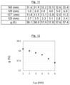
- the last line of the table of the figure 9 , as well as the figure 10 illustrate the evolution, in ordinate in figure 10 , of the solar factor, g, in percent, as a function of the thickness, t 129 , in nanometers of the zinc-based oxide sublayer ZnO 129 on the abscissa, this solar factor being measured immediately after the laser treatment of the two substrates 10, 30, then their integration to form the triple glazing.
- the solar factor is thus improved when the zinc-based oxide sublayer ZnO 129 is between 0.3 and 4.4 nm.
- the solar factor is particularly favorable for a thickness of this zinc-based oxide sublayer ZnO 129 between 1.0 and 3.0 nm, or even between 1.5 and 2.4 nm.
- the solar factor of the triple glazing rose to 58.1%; i.e. a gain of + 0.5 in solar factor by reducing the thickness of the zinc-based oxide sublayer ZnO 129 from 5.0 nm to 1.0 nm; this gain can be further increased by further reducing the thickness of the zinc-based oxide sublayer ZnO 129 to 0.5 nm, or even 0.3 nm.
- the inner substrate 30 of this double glazing is coated on its inner face 29 facing the intermediate gas blade 15 with an insulating coating 14 consisting of the functional single-layer stack described above: the functional single-layer stack are thus on the face called “face 3”).
- the table of the figure 11 summarizes the exact thickness of layers 125, 127', 129 and 165, in nm, for the 6 examples of zinc-based oxide underlayer ZnO 129, with a physical thickness varying from 1.0 nm to 6.0 nm.
- the last line of the table of the figure 11 illustrates the evolution on the ordinate of the solar factor, g, in percent, as a function of the thickness, t 129 , in nanometers of this sublayer of zinc-based oxide ZnO 129 on the abscissa, this solar factor being measured immediately after the laser treatment of the two substrates 10, 30, then their integration to form the triple glazing.
- the solar factor increases from 57.4% for a glazing whose stack comprises a sublayer of zinc-based oxide ZnO 129 of 6.0 nm to 58.1% for a glazing whose stack comprises a sublayer of zinc-based oxide ZnO 129 of 1.0 nm; the solar factor is thus clearly improved, in an unexpected manner, when the sublayer of zinc-based oxide ZnO 129 is between 0.3 and 4.4 nm.
- the solar factor is particularly favorable for a thickness of zinc-based oxide underlayer ZnO 129 between 0.3 and 2.9 nm, or even between 0.5 and 2.4.
Landscapes
- Chemical & Material Sciences (AREA)
- Life Sciences & Earth Sciences (AREA)
- Engineering & Computer Science (AREA)
- Chemical Kinetics & Catalysis (AREA)
- General Chemical & Material Sciences (AREA)
- Geochemistry & Mineralogy (AREA)
- Materials Engineering (AREA)
- Organic Chemistry (AREA)
- Laminated Bodies (AREA)
- Surface Treatment Of Glass (AREA)
- Chemical Vapour Deposition (AREA)
Claims (12)
- Material, umfassend ein Glassubstrat (30), das auf einer Fläche (29) mit einer Stapelung von Dünnschichten (14) mit Reflexionseigenschaften in dem Infrarot- und/oder in dem Sonnenstrahlungsbereich beschichtet ist, die mindestens eine funktionelle Metallschicht (140), insbesondere auf Basis von Silber oder einer Metalllegierung, die Silber enthält, und mindestens zwei Antireflexbeschichtungen (120, 160) aufweist, wobei die Antireflexbeschichtungen jeweils mindestens eine dielektrische Schicht (125, 165) aufweisen, wobei die funktionelle Schicht (140) zwischen den zwei Antireflexbeschichtungen (120, 160) angeordnet ist, dadurch gekennzeichnet, dass die darunterliegende Antireflexbeschichtung (120), die unter der funktionellen Schicht (140) in Richtung des Substrats (30) gelegen ist, aufweist: - eine Unterschicht aus Oxid auf Basis von Zink ZnO (129), die unter und in Kontakt mit der funktionellen Schicht (140) gelegen ist, mit einer physikalischen Dicke der Unterschicht aus Oxid auf Basis von Zink ZnO (129), die zwischen 0,3 und 4,4 nm, oder sogar zwischen 0,3 und 2,9 nm, oder sogar zwischen 0,5 und 2,4 nm liegt;- eine dielektrische Unterschicht aus Mischoxid auf Basis von Zink und Zinn SniZnjO (128), mit einer physikalischen Dicke der dielektrischen Unterschicht aus Mischoxid auf Basis von Zink und Zinn SniZnjO (128), die zwischen 3,0 und 50,0 nm oder sogar zwischen 4,0 und 40,0 nm oder sogar zwischen 5,0 und 35,0 nm liegt;- eine dielektrische Unterschicht aus Nitrid auf Basis von Silizium Si3N4 (127) oder auf Basis von Siliziumzirkonium SixNyZrz (127'), die unter und in Kontakt mit der dielektrischen Unterschicht aus Oxid auf Basis von Zink und Zinn SniZnjO (128) gelegen ist, mit einer physikalischen Dicke der dielektrischen Unterschicht aus Nitrid auf Basis von Silizium SI3N4 (127) oder auf Basis von Siliziumzirkonium SixNyZrz (127'), die zwischen 5,0 und 50,0 nm oder sogar zwischen 10,0 und 40,0 nm oder sogar zwischen 15,0 und 25,0 nm liegt;dass die darüberliegende Antireflexbeschichtung (160), die über der funktionellen Schicht (140) gegenüber dem Substrat (30) gelegen ist, aufweist:- eine Überschicht aus Oxid auf Basis von Zink ZnO (161) mit einer physikalischen Dicke der Überschicht aus Oxid auf Basis von Zink ZnO (161), die zwischen 2,0 und 10,0 nm oder sogar zwischen 2,0 und 8,0 nm oder sogar zwischen 2,5 und 5,4 nm liegt; und- eine dielektrische Überschicht (165), die auf der Überschicht aus Oxid auf Basis von Zink ZnO (161) gelegen ist, und vorzugsweise eine dielektrische Überschicht aus Nitrid auf Basis von Silizium, Si3N4,und dass eine Überblockierungsschicht aus Oxid auf Basis von Titan TiOx (150) auf und in Kontakt mit der funktionellen Schicht (140) und unter der darüberliegenden Antireflexbeschichtung (160) gelegen ist, mit einer physikalischen Dicke der Blockierungsschicht aus Oxid auf Basis von Titan TiOx (150), die zwischen 0,3 und 5,0 nm, sogar zwischen 0,3 und 2,9 nm oder sogar zwischen 0,5 und 2,4 nm liegt.
- Material nach Anspruch 1, wobei die dielektrische Unterschicht aus Nitrid auf Basis von Siliziumzirkonium SixNyZrz (127') ist und ein Atomverhältnis von Silizium zu Zirkonium, x/z, zwischen 2,2 und 5,6 oder sogar zwischen 2,9 und 5,6 oder sogar zwischen 3,0 und 4,8 vorweist, wobei die dielektrische Unterschicht aus Nitrid auf Basis von Siliziumzirkonium SixNyZrz (127') vorzugsweise keinen Sauerstoff aufweist.
- Material nach Anspruch 1 oder 2, wobei die funktionelle Metallschicht (140) oder jede metallische Funktion eine physikalische Dicke vorweist, die zwischen 8,0 und 22,0 nm oder sogar zwischen 9,0 und 16,4 nm oder sogar zwischen 9,5 und 12,4 nm liegt.
- Material nach einem der Ansprüche 1 bis 3, wobei die darunterliegende Antireflexbeschichtung (120), die unter der funktionellen Metallschicht (140) gelegen ist und/oder die darüberliegende Antireflexbeschichtung (160), die über der funktionellen Metallschicht (140) gelegen ist, überhaupt keine Schicht in dem metallischen Zustand aufweist.
- Material nach einem der Ansprüche 1 bis 4, wobei die Unterschicht aus Nitrid auf Basis von Siliziumzirkonium SixNyZrz (127') ist und eine primäre dielektrische Unterschicht aus Nitrid auf Basis von Silizium Si3N4 (125) unter und in Kontakt mit dieser Unterschicht aus Nitrid auf Basis von Siliziumzirkonium SixNyZrz (127') gelegen ist, mit einer physikalischen Dicke der primären dielektrischen Unterschicht aus Nitrid auf Basis von Silizium Si3N4 (125), die zwischen 5,0 und 30,0 nm oder sogar zwischen 5,0 und 20,0 nm oder sogar zwischen 5,0 und 10,0 nm liegt.
- Material nach Anspruch 1, wobei die dielektrische Unterschicht aus Nitrid auf Basis von Silizium Si3N4 (127) ist und keinen Sauerstoff aufweist.
- Material nach einem der Ansprüche 1 bis 6, wobei die Unterschicht aus Oxid auf Basis von Zink ZnO (129) und/oder die Überschicht aus Oxid auf Basis von Zink ZnO (161) aus mit Aluminium dotiertem Zinkoxid ZnO besteht.
- Material nach einem der Ansprüche 1 bis 7, wobei die darüberliegende Antireflexbeschichtung (160), die über der funktionellen Schicht (140) gelegen ist, ferner eine dielektrische Zwischenüberschicht (163) umfasst, die zwischen der Überschicht auf Basis von Zinkoxid ZnO (161) und der dielektrischen Überschicht (165) gelegen ist, wobei diese dielektrische Zwischenüberschicht (163) oxidiert ist und vorzugsweise umfasst: ein Titanoxid TiOx oder ein Mischoxid aus Zink und aus Zinn.
- Mehrfachverglasung, die mindestens ein Material nach einem der Ansprüche 1 bis 8 und mindestens ein anderes Substrat (10) aufweist, wobei die Substrate (10, 30) durch eine Rahmenstruktur (90) zusammengehalten werden, wobei die Verglasung eine Trennung zwischen einem Außenraum (ES) und einem Innenraum (IS) herstellt, wobei mindestens ein Zwischenlagengasspalt (15) zwischen den zwei Substraten angeordnet ist.
- Verfahren zum Gewinnen eines Materials, das ein Glassubstrat (30) aufweist, das auf einer Fläche (29) mit einer Stapelung von Dünnschichten (14) mit Reflexionseigenschaften in dem Infrarot- und/oder in dem Sonnenstrahlungsbereich beschichtet ist, die mindestens eine funktionelle Metallschicht (140), insbesondere auf Basis von Silber oder einer Metalllegierung, die Silber enthält, und zwei Antireflexbeschichtungen (120, 160) aufweist, wobei die Antireflexbeschichtungen jeweils mindestens eine dielektrische Schicht (127, 165) aufweisen, wobei die funktionelle Schicht (140) zwischen den zwei Antireflexbeschichtungen (120, 160) angeordnet ist, das Verfahren umfassend die folgenden Schritte der Reihe nach:- Abscheiden auf eine Fläche (29) des Substrats (30) einer Stapelung von Dünnschichten (14) mit Reflexionseigenschaften in dem Infrarot- und/oder in dem Sonnenstrahlungsbereich, die mindestens eine funktionelle Metallschicht (140), insbesondere auf Basis von Silber oder einer Metalllegierung, die Silber enthält, und mindestens zwei Antireflexbeschichtungen (120, 160) aufweist, um ein Material nach einem der Ansprüche 1 bis 8 auszubilden, dann- Behandeln der Stapelung von Dünnschichten (14) mithilfe einer Quelle, die eine Strahlung und insbesondere eine Infrarotstrahlung produziert.
- Verfahren nach Anspruch 10, wobei das Behandeln in einer Atmosphäre durchgeführt wird, umfassend keinen Sauerstoff.
- Verfahren nach Anspruch 10 oder 11, wobei die Unterschicht aus Oxid auf Basis von Zink ZnO (129) von einem Keramikziel, umfassend ZnO, und in einer Atmosphäre, die keinen Sauerstoff aufweist oder mehr als 10,0 % Sauerstoff aufweist, abgeschieden wird.
Applications Claiming Priority (2)
| Application Number | Priority Date | Filing Date | Title |
|---|---|---|---|
| FR2013685A FR3117929B1 (fr) | 2020-12-18 | 2020-12-18 | Materiau comportant un empilement a sous-couche dielectrique fine d’oxide a base de zinc et procede de depot de ce materiau |
| PCT/FR2021/052360 WO2022129797A1 (fr) | 2020-12-18 | 2021-12-16 | Matériau comportant un empilement à sous-couche diéléctrique fine d'oxide à base de zinc et procédé de dépot de ce matériau |
Publications (2)
| Publication Number | Publication Date |
|---|---|
| EP4263455A1 EP4263455A1 (de) | 2023-10-25 |
| EP4263455B1 true EP4263455B1 (de) | 2024-11-06 |
Family
ID=75690330
Family Applications (1)
| Application Number | Title | Priority Date | Filing Date |
|---|---|---|---|
| EP21851971.8A Active EP4263455B1 (de) | 2020-12-18 | 2021-12-16 | Material mit einem stapel mit einer dünnen, dielektrischen oxidunterschicht auf zinkbasis und verfahren zur abscheidung dieses materials |
Country Status (4)
| Country | Link |
|---|---|
| EP (1) | EP4263455B1 (de) |
| FR (1) | FR3117929B1 (de) |
| PL (1) | PL4263455T3 (de) |
| WO (1) | WO2022129797A1 (de) |
Citations (1)
| Publication number | Priority date | Publication date | Assignee | Title |
|---|---|---|---|---|
| FR2919110A1 (fr) * | 2007-07-16 | 2009-01-23 | Saint Gobain | Substrat de face avant d'ecran plasma, utilisation et procede de fabrication |
Family Cites Families (5)
| Publication number | Priority date | Publication date | Assignee | Title |
|---|---|---|---|---|
| FR2728559B1 (fr) | 1994-12-23 | 1997-01-31 | Saint Gobain Vitrage | Substrats en verre revetus d'un empilement de couches minces a proprietes de reflexion dans l'infrarouge et/ou dans le domaine du rayonnement solaire |
| FR2946639B1 (fr) | 2009-06-12 | 2011-07-15 | Saint Gobain | Procede de depot de couche mince et produit obtenu. |
| GB201102724D0 (en) * | 2011-02-17 | 2011-03-30 | Pilkington Group Ltd | Heat treatable coated glass pane |
| FR3026404B1 (fr) * | 2014-09-30 | 2016-11-25 | Saint Gobain | Substrat muni d'un empilement a proprietes thermiques et a couche intermediaire sous stoechiometrique |
| FR3054892A1 (fr) * | 2016-08-02 | 2018-02-09 | Saint Gobain | Substrat muni d'un empilement a proprietes thermiques comportant au moins une couche comprenant du nitrure de silicium-zirconium enrichi en zirconium, son utilisation et sa fabrication. |
-
2020
- 2020-12-18 FR FR2013685A patent/FR3117929B1/fr active Active
-
2021
- 2021-12-16 PL PL21851971.8T patent/PL4263455T3/pl unknown
- 2021-12-16 EP EP21851971.8A patent/EP4263455B1/de active Active
- 2021-12-16 WO PCT/FR2021/052360 patent/WO2022129797A1/fr not_active Ceased
Patent Citations (1)
| Publication number | Priority date | Publication date | Assignee | Title |
|---|---|---|---|---|
| FR2919110A1 (fr) * | 2007-07-16 | 2009-01-23 | Saint Gobain | Substrat de face avant d'ecran plasma, utilisation et procede de fabrication |
Also Published As
| Publication number | Publication date |
|---|---|
| PL4263455T3 (pl) | 2025-03-24 |
| WO2022129797A1 (fr) | 2022-06-23 |
| FR3117929A1 (fr) | 2022-06-24 |
| FR3117929B1 (fr) | 2023-12-29 |
| EP4263455A1 (de) | 2023-10-25 |
Similar Documents
| Publication | Publication Date | Title |
|---|---|---|
| EP3494420B1 (de) | Substrat mit einem stapel mit thermischen eigenschaften mit mindestens einer schicht mit zirkoniumreichem silicium-zirkonium-nitrid, verwendung und herstellung davon | |
| WO2005019126A1 (fr) | Substrat transparent revetu d'un empilement de couches minces a proprietes de reflexion dans l'infrarouge et/ou dans le domaine du rayonnement solaire | |
| EP3201150B1 (de) | Substrat mit einer mehrfachschicht mit thermischen eigenschaften und einer substöchiometrischen zwischenschicht | |
| EP4229017B1 (de) | Material mit einem stapel mit eingeschlossener metallischer absorptionsschicht und verfahren zur ablagerung dieses materials | |
| EP4172123A1 (de) | Material mit einem stapel mit einer dünnen dielektrischen schicht aus zinkbasiertem oxid und verfahren zur anwendung des besagten materials | |
| FR3036701A1 (fr) | Substrat muni d'un empilement a proprietes thermiques a couche terminale metallique et a couche preterminale oxydee | |
| EP4065531A1 (de) | Material mit einem stapel mit einer dünnen dielektrischen unterschicht aus zinkoxid und verfahren zur abscheidung dieses materials | |
| CA3006338A1 (fr) | Substrat muni d'un empilement a proprietes thermiques comportant au moins une couche en oxyde de nickel | |
| EP4263455B1 (de) | Material mit einem stapel mit einer dünnen, dielektrischen oxidunterschicht auf zinkbasis und verfahren zur abscheidung dieses materials | |
| EP4263456B1 (de) | Material mit einem stapel mit einer dünnen, dielektrischen oxidunterschicht auf zinkbasis und verfahren zur abscheidung dieses materials | |
| EP4065530B1 (de) | Material mit einem stapel mit einer dünnen dielektrischen oxidunterschicht auf zinkbasis und verfahren zum aufbringen dieses materials | |
| FR3111891A1 (fr) | Materiau comportant un empilement a sous-couche dielectrique fine d’oxide a base de zinc et procede de depot de ce materiau | |
| FR3109776A1 (fr) | Materiau comportant un empilement a sous-couche dielectrique fine d’oxide a base de zinc et procede de depot de ce materiau | |
| EP4172122A1 (de) | Material mit einem stapel mit einer dünnen dielektrischen schicht aus zinkbasiertem oxid und verfahren zur abscheidung dieses materials | |
| FR3114264A1 (fr) | Materiau comportant un empilement a couche metallique absorbante et surcouche dielectrique et procede de depot de ce materiau | |
| WO2024056765A1 (fr) | Materiau comportant un empilement comprenant un module de six couches | |
| WO2023180127A1 (fr) | Materiau comportant un empilement a couche absorbante metallique et procede de depot de ce materiau | |
| FR3157264A1 (fr) | Utilisation d’un vitrage multiple reversible et vitrage multiple pour l’utilisation | |
| CA3006339A1 (fr) | Substrat muni d'un empilement a proprietes thermiques comportant au moins une couche en oxyde de nickel |
Legal Events
| Date | Code | Title | Description |
|---|---|---|---|
| STAA | Information on the status of an ep patent application or granted ep patent |
Free format text: STATUS: UNKNOWN |
|
| STAA | Information on the status of an ep patent application or granted ep patent |
Free format text: STATUS: THE INTERNATIONAL PUBLICATION HAS BEEN MADE |
|
| PUAI | Public reference made under article 153(3) epc to a published international application that has entered the european phase |
Free format text: ORIGINAL CODE: 0009012 |
|
| STAA | Information on the status of an ep patent application or granted ep patent |
Free format text: STATUS: REQUEST FOR EXAMINATION WAS MADE |
|
| 17P | Request for examination filed |
Effective date: 20230718 |
|
| AK | Designated contracting states |
Kind code of ref document: A1 Designated state(s): AL AT BE BG CH CY CZ DE DK EE ES FI FR GB GR HR HU IE IS IT LI LT LU LV MC MK MT NL NO PL PT RO RS SE SI SK SM TR |
|
| DAV | Request for validation of the european patent (deleted) | ||
| DAX | Request for extension of the european patent (deleted) | ||
| GRAP | Despatch of communication of intention to grant a patent |
Free format text: ORIGINAL CODE: EPIDOSNIGR1 |
|
| STAA | Information on the status of an ep patent application or granted ep patent |
Free format text: STATUS: GRANT OF PATENT IS INTENDED |
|
| INTG | Intention to grant announced |
Effective date: 20240605 |
|
| GRAS | Grant fee paid |
Free format text: ORIGINAL CODE: EPIDOSNIGR3 |
|
| GRAA | (expected) grant |
Free format text: ORIGINAL CODE: 0009210 |
|
| STAA | Information on the status of an ep patent application or granted ep patent |
Free format text: STATUS: THE PATENT HAS BEEN GRANTED |
|
| AK | Designated contracting states |
Kind code of ref document: B1 Designated state(s): AL AT BE BG CH CY CZ DE DK EE ES FI FR GB GR HR HU IE IS IT LI LT LU LV MC MK MT NL NO PL PT RO RS SE SI SK SM TR |
|
| REG | Reference to a national code |
Ref country code: GB Ref legal event code: FG4D Free format text: NOT ENGLISH |
|
| REG | Reference to a national code |
Ref country code: CH Ref legal event code: EP |
|
| REG | Reference to a national code |
Ref country code: DE Ref legal event code: R096 Ref document number: 602021021612 Country of ref document: DE |
|
| REG | Reference to a national code |
Ref country code: IE Ref legal event code: FG4D Free format text: LANGUAGE OF EP DOCUMENT: FRENCH |
|
| P01 | Opt-out of the competence of the unified patent court (upc) registered |
Free format text: CASE NUMBER: APP_65800/2024 Effective date: 20241212 |
|
| REG | Reference to a national code |
Ref country code: LT Ref legal event code: MG9D |
|
| REG | Reference to a national code |
Ref country code: NL Ref legal event code: MP Effective date: 20241106 |
|
| PG25 | Lapsed in a contracting state [announced via postgrant information from national office to epo] |
Ref country code: IS Free format text: LAPSE BECAUSE OF FAILURE TO SUBMIT A TRANSLATION OF THE DESCRIPTION OR TO PAY THE FEE WITHIN THE PRESCRIBED TIME-LIMIT Effective date: 20250306 Ref country code: HR Free format text: LAPSE BECAUSE OF FAILURE TO SUBMIT A TRANSLATION OF THE DESCRIPTION OR TO PAY THE FEE WITHIN THE PRESCRIBED TIME-LIMIT Effective date: 20241106 Ref country code: PT Free format text: LAPSE BECAUSE OF FAILURE TO SUBMIT A TRANSLATION OF THE DESCRIPTION OR TO PAY THE FEE WITHIN THE PRESCRIBED TIME-LIMIT Effective date: 20250306 |
|
| PG25 | Lapsed in a contracting state [announced via postgrant information from national office to epo] |
Ref country code: NL Free format text: LAPSE BECAUSE OF FAILURE TO SUBMIT A TRANSLATION OF THE DESCRIPTION OR TO PAY THE FEE WITHIN THE PRESCRIBED TIME-LIMIT Effective date: 20241106 Ref country code: FI Free format text: LAPSE BECAUSE OF FAILURE TO SUBMIT A TRANSLATION OF THE DESCRIPTION OR TO PAY THE FEE WITHIN THE PRESCRIBED TIME-LIMIT Effective date: 20241106 |
|
| REG | Reference to a national code |
Ref country code: AT Ref legal event code: MK05 Ref document number: 1739226 Country of ref document: AT Kind code of ref document: T Effective date: 20241106 |
|
| PG25 | Lapsed in a contracting state [announced via postgrant information from national office to epo] |
Ref country code: BG Free format text: LAPSE BECAUSE OF FAILURE TO SUBMIT A TRANSLATION OF THE DESCRIPTION OR TO PAY THE FEE WITHIN THE PRESCRIBED TIME-LIMIT Effective date: 20241106 |
|
| PG25 | Lapsed in a contracting state [announced via postgrant information from national office to epo] |
Ref country code: ES Free format text: LAPSE BECAUSE OF FAILURE TO SUBMIT A TRANSLATION OF THE DESCRIPTION OR TO PAY THE FEE WITHIN THE PRESCRIBED TIME-LIMIT Effective date: 20241106 |
|
| PG25 | Lapsed in a contracting state [announced via postgrant information from national office to epo] |
Ref country code: NO Free format text: LAPSE BECAUSE OF FAILURE TO SUBMIT A TRANSLATION OF THE DESCRIPTION OR TO PAY THE FEE WITHIN THE PRESCRIBED TIME-LIMIT Effective date: 20250206 |
|
| PG25 | Lapsed in a contracting state [announced via postgrant information from national office to epo] |
Ref country code: LV Free format text: LAPSE BECAUSE OF FAILURE TO SUBMIT A TRANSLATION OF THE DESCRIPTION OR TO PAY THE FEE WITHIN THE PRESCRIBED TIME-LIMIT Effective date: 20241106 Ref country code: GR Free format text: LAPSE BECAUSE OF FAILURE TO SUBMIT A TRANSLATION OF THE DESCRIPTION OR TO PAY THE FEE WITHIN THE PRESCRIBED TIME-LIMIT Effective date: 20250207 Ref country code: AT Free format text: LAPSE BECAUSE OF FAILURE TO SUBMIT A TRANSLATION OF THE DESCRIPTION OR TO PAY THE FEE WITHIN THE PRESCRIBED TIME-LIMIT Effective date: 20241106 |
|
| PG25 | Lapsed in a contracting state [announced via postgrant information from national office to epo] |
Ref country code: RS Free format text: LAPSE BECAUSE OF FAILURE TO SUBMIT A TRANSLATION OF THE DESCRIPTION OR TO PAY THE FEE WITHIN THE PRESCRIBED TIME-LIMIT Effective date: 20250206 |
|
| PG25 | Lapsed in a contracting state [announced via postgrant information from national office to epo] |
Ref country code: SM Free format text: LAPSE BECAUSE OF FAILURE TO SUBMIT A TRANSLATION OF THE DESCRIPTION OR TO PAY THE FEE WITHIN THE PRESCRIBED TIME-LIMIT Effective date: 20241106 |
|
| PG25 | Lapsed in a contracting state [announced via postgrant information from national office to epo] |
Ref country code: DK Free format text: LAPSE BECAUSE OF FAILURE TO SUBMIT A TRANSLATION OF THE DESCRIPTION OR TO PAY THE FEE WITHIN THE PRESCRIBED TIME-LIMIT Effective date: 20241106 |
|
| PG25 | Lapsed in a contracting state [announced via postgrant information from national office to epo] |
Ref country code: EE Free format text: LAPSE BECAUSE OF FAILURE TO SUBMIT A TRANSLATION OF THE DESCRIPTION OR TO PAY THE FEE WITHIN THE PRESCRIBED TIME-LIMIT Effective date: 20241106 |
|
| PG25 | Lapsed in a contracting state [announced via postgrant information from national office to epo] |
Ref country code: RO Free format text: LAPSE BECAUSE OF FAILURE TO SUBMIT A TRANSLATION OF THE DESCRIPTION OR TO PAY THE FEE WITHIN THE PRESCRIBED TIME-LIMIT Effective date: 20241106 |
|
| PG25 | Lapsed in a contracting state [announced via postgrant information from national office to epo] |
Ref country code: SK Free format text: LAPSE BECAUSE OF FAILURE TO SUBMIT A TRANSLATION OF THE DESCRIPTION OR TO PAY THE FEE WITHIN THE PRESCRIBED TIME-LIMIT Effective date: 20241106 |
|
| PG25 | Lapsed in a contracting state [announced via postgrant information from national office to epo] |
Ref country code: CZ Free format text: LAPSE BECAUSE OF FAILURE TO SUBMIT A TRANSLATION OF THE DESCRIPTION OR TO PAY THE FEE WITHIN THE PRESCRIBED TIME-LIMIT Effective date: 20241106 |
|
| PG25 | Lapsed in a contracting state [announced via postgrant information from national office to epo] |
Ref country code: IT Free format text: LAPSE BECAUSE OF FAILURE TO SUBMIT A TRANSLATION OF THE DESCRIPTION OR TO PAY THE FEE WITHIN THE PRESCRIBED TIME-LIMIT Effective date: 20241106 |
|
| REG | Reference to a national code |
Ref country code: CH Ref legal event code: PL |
|
| REG | Reference to a national code |
Ref country code: DE Ref legal event code: R097 Ref document number: 602021021612 Country of ref document: DE |
|
| PG25 | Lapsed in a contracting state [announced via postgrant information from national office to epo] |
Ref country code: LU Free format text: LAPSE BECAUSE OF NON-PAYMENT OF DUE FEES Effective date: 20241216 |
|
| PG25 | Lapsed in a contracting state [announced via postgrant information from national office to epo] |
Ref country code: SE Free format text: LAPSE BECAUSE OF FAILURE TO SUBMIT A TRANSLATION OF THE DESCRIPTION OR TO PAY THE FEE WITHIN THE PRESCRIBED TIME-LIMIT Effective date: 20241106 |
|
| PLBE | No opposition filed within time limit |
Free format text: ORIGINAL CODE: 0009261 |
|
| STAA | Information on the status of an ep patent application or granted ep patent |
Free format text: STATUS: NO OPPOSITION FILED WITHIN TIME LIMIT |
|
| PG25 | Lapsed in a contracting state [announced via postgrant information from national office to epo] |
Ref country code: MC Free format text: LAPSE BECAUSE OF FAILURE TO SUBMIT A TRANSLATION OF THE DESCRIPTION OR TO PAY THE FEE WITHIN THE PRESCRIBED TIME-LIMIT Effective date: 20241106 |
|
| REG | Reference to a national code |
Ref country code: BE Ref legal event code: MM Effective date: 20241231 |
|
| 26N | No opposition filed |
Effective date: 20250807 |
|
| PG25 | Lapsed in a contracting state [announced via postgrant information from national office to epo] |
Ref country code: BE Free format text: LAPSE BECAUSE OF NON-PAYMENT OF DUE FEES Effective date: 20241231 |
|
| PG25 | Lapsed in a contracting state [announced via postgrant information from national office to epo] |
Ref country code: CH Free format text: LAPSE BECAUSE OF NON-PAYMENT OF DUE FEES Effective date: 20241231 |
|
| PG25 | Lapsed in a contracting state [announced via postgrant information from national office to epo] |
Ref country code: IE Free format text: LAPSE BECAUSE OF NON-PAYMENT OF DUE FEES Effective date: 20241216 |
|
| PGFP | Annual fee paid to national office [announced via postgrant information from national office to epo] |
Ref country code: DE Payment date: 20251104 Year of fee payment: 5 |
|
| PGFP | Annual fee paid to national office [announced via postgrant information from national office to epo] |
Ref country code: GB Payment date: 20251030 Year of fee payment: 5 |
|
| PGFP | Annual fee paid to national office [announced via postgrant information from national office to epo] |
Ref country code: FR Payment date: 20251110 Year of fee payment: 5 |
|
| PGFP | Annual fee paid to national office [announced via postgrant information from national office to epo] |
Ref country code: PL Payment date: 20251105 Year of fee payment: 5 |