EP4274704B1 - Verfahren zum verbinden eines ersten teils und eines zweiten teils durch direkthartlöten, einschliesslich stufen zur vorbereitung der oberfläche von mindestens einem der teile - Google Patents
Verfahren zum verbinden eines ersten teils und eines zweiten teils durch direkthartlöten, einschliesslich stufen zur vorbereitung der oberfläche von mindestens einem der teile Download PDFInfo
- Publication number
- EP4274704B1 EP4274704B1 EP22702754.7A EP22702754A EP4274704B1 EP 4274704 B1 EP4274704 B1 EP 4274704B1 EP 22702754 A EP22702754 A EP 22702754A EP 4274704 B1 EP4274704 B1 EP 4274704B1
- Authority
- EP
- European Patent Office
- Prior art keywords
- layer
- carbon
- brazing
- active element
- active
- Prior art date
- Legal status (The legal status is an assumption and is not a legal conclusion. Google has not performed a legal analysis and makes no representation as to the accuracy of the status listed.)
- Active
Links
Images


Classifications
-
- B—PERFORMING OPERATIONS; TRANSPORTING
- B23—MACHINE TOOLS; METAL-WORKING NOT OTHERWISE PROVIDED FOR
- B23K—SOLDERING OR UNSOLDERING; WELDING; CLADDING OR PLATING BY SOLDERING OR WELDING; CUTTING BY APPLYING HEAT LOCALLY, e.g. FLAME CUTTING; WORKING BY LASER BEAM
- B23K1/00—Soldering, e.g. brazing, or unsoldering
- B23K1/19—Soldering, e.g. brazing, or unsoldering taking account of the properties of the materials to be soldered
-
- B—PERFORMING OPERATIONS; TRANSPORTING
- B23—MACHINE TOOLS; METAL-WORKING NOT OTHERWISE PROVIDED FOR
- B23K—SOLDERING OR UNSOLDERING; WELDING; CLADDING OR PLATING BY SOLDERING OR WELDING; CUTTING BY APPLYING HEAT LOCALLY, e.g. FLAME CUTTING; WORKING BY LASER BEAM
- B23K1/00—Soldering, e.g. brazing, or unsoldering
- B23K1/0008—Soldering, e.g. brazing, or unsoldering specially adapted for particular articles or work
-
- B—PERFORMING OPERATIONS; TRANSPORTING
- B23—MACHINE TOOLS; METAL-WORKING NOT OTHERWISE PROVIDED FOR
- B23K—SOLDERING OR UNSOLDERING; WELDING; CLADDING OR PLATING BY SOLDERING OR WELDING; CUTTING BY APPLYING HEAT LOCALLY, e.g. FLAME CUTTING; WORKING BY LASER BEAM
- B23K1/00—Soldering, e.g. brazing, or unsoldering
- B23K1/20—Preliminary treatment of work or areas to be soldered, e.g. in respect of a galvanic coating
-
- B—PERFORMING OPERATIONS; TRANSPORTING
- B23—MACHINE TOOLS; METAL-WORKING NOT OTHERWISE PROVIDED FOR
- B23K—SOLDERING OR UNSOLDERING; WELDING; CLADDING OR PLATING BY SOLDERING OR WELDING; CUTTING BY APPLYING HEAT LOCALLY, e.g. FLAME CUTTING; WORKING BY LASER BEAM
- B23K1/00—Soldering, e.g. brazing, or unsoldering
- B23K1/20—Preliminary treatment of work or areas to be soldered, e.g. in respect of a galvanic coating
- B23K1/206—Cleaning
-
- B—PERFORMING OPERATIONS; TRANSPORTING
- B23—MACHINE TOOLS; METAL-WORKING NOT OTHERWISE PROVIDED FOR
- B23K—SOLDERING OR UNSOLDERING; WELDING; CLADDING OR PLATING BY SOLDERING OR WELDING; CUTTING BY APPLYING HEAT LOCALLY, e.g. FLAME CUTTING; WORKING BY LASER BEAM
- B23K35/00—Rods, electrodes, materials, or media, for use in soldering, welding, or cutting
- B23K35/22—Rods, electrodes, materials, or media, for use in soldering, welding, or cutting characterised by the composition or nature of the material
- B23K35/24—Selection of soldering or welding materials proper
- B23K35/26—Selection of soldering or welding materials proper with the principal constituent melting at less than 400°C
- B23K35/262—Sn as the principal constituent
-
- B—PERFORMING OPERATIONS; TRANSPORTING
- B23—MACHINE TOOLS; METAL-WORKING NOT OTHERWISE PROVIDED FOR
- B23K—SOLDERING OR UNSOLDERING; WELDING; CLADDING OR PLATING BY SOLDERING OR WELDING; CUTTING BY APPLYING HEAT LOCALLY, e.g. FLAME CUTTING; WORKING BY LASER BEAM
- B23K2103/00—Materials to be soldered, welded or cut
- B23K2103/08—Non-ferrous metals or alloys
- B23K2103/14—Titanium or alloys thereof
-
- B—PERFORMING OPERATIONS; TRANSPORTING
- B23—MACHINE TOOLS; METAL-WORKING NOT OTHERWISE PROVIDED FOR
- B23K—SOLDERING OR UNSOLDERING; WELDING; CLADDING OR PLATING BY SOLDERING OR WELDING; CUTTING BY APPLYING HEAT LOCALLY, e.g. FLAME CUTTING; WORKING BY LASER BEAM
- B23K2103/00—Materials to be soldered, welded or cut
- B23K2103/16—Composite materials
-
- B—PERFORMING OPERATIONS; TRANSPORTING
- B23—MACHINE TOOLS; METAL-WORKING NOT OTHERWISE PROVIDED FOR
- B23K—SOLDERING OR UNSOLDERING; WELDING; CLADDING OR PLATING BY SOLDERING OR WELDING; CUTTING BY APPLYING HEAT LOCALLY, e.g. FLAME CUTTING; WORKING BY LASER BEAM
- B23K2103/00—Materials to be soldered, welded or cut
- B23K2103/16—Composite materials
- B23K2103/166—Multilayered materials
- B23K2103/172—Multilayered materials wherein at least one of the layers is non-metallic
-
- B—PERFORMING OPERATIONS; TRANSPORTING
- B23—MACHINE TOOLS; METAL-WORKING NOT OTHERWISE PROVIDED FOR
- B23K—SOLDERING OR UNSOLDERING; WELDING; CLADDING OR PLATING BY SOLDERING OR WELDING; CUTTING BY APPLYING HEAT LOCALLY, e.g. FLAME CUTTING; WORKING BY LASER BEAM
- B23K2103/00—Materials to be soldered, welded or cut
- B23K2103/18—Dissimilar materials
-
- B—PERFORMING OPERATIONS; TRANSPORTING
- B23—MACHINE TOOLS; METAL-WORKING NOT OTHERWISE PROVIDED FOR
- B23K—SOLDERING OR UNSOLDERING; WELDING; CLADDING OR PLATING BY SOLDERING OR WELDING; CUTTING BY APPLYING HEAT LOCALLY, e.g. FLAME CUTTING; WORKING BY LASER BEAM
- B23K2103/00—Materials to be soldered, welded or cut
- B23K2103/18—Dissimilar materials
- B23K2103/26—Alloys of Nickel and Cobalt and Chromium
-
- B—PERFORMING OPERATIONS; TRANSPORTING
- B23—MACHINE TOOLS; METAL-WORKING NOT OTHERWISE PROVIDED FOR
- B23K—SOLDERING OR UNSOLDERING; WELDING; CLADDING OR PLATING BY SOLDERING OR WELDING; CUTTING BY APPLYING HEAT LOCALLY, e.g. FLAME CUTTING; WORKING BY LASER BEAM
- B23K2103/00—Materials to be soldered, welded or cut
- B23K2103/30—Organic materials
-
- B—PERFORMING OPERATIONS; TRANSPORTING
- B23—MACHINE TOOLS; METAL-WORKING NOT OTHERWISE PROVIDED FOR
- B23K—SOLDERING OR UNSOLDERING; WELDING; CLADDING OR PLATING BY SOLDERING OR WELDING; CUTTING BY APPLYING HEAT LOCALLY, e.g. FLAME CUTTING; WORKING BY LASER BEAM
- B23K2103/00—Materials to be soldered, welded or cut
- B23K2103/50—Inorganic materials other than metals or composite materials
Definitions
- the present invention relates to the general field of brazing and more particularly to a method of direct brazing of a first part and a second part, see claim 1.
- the invention is particularly interesting since it allows the direct assembly by soft soldering (typically for temperatures below 450°C) of two parts using non-active solders.
- the invention finds applications in the field of implants, for example prostheses.
- tin-based alloys such as Sn-Ag-Cu-Cr, Sn-Ag-Cu, or Sn-Ag-Cu-Ni are used for brazing carbon nanotubes to a copper element.
- the process is carried out at temperatures below 700°C. This process is used to produce small devices, in this case electrical components. Such devices involve low deformations and therefore low thermomechanical stresses. Brazing is further facilitated by the use of copper, which is very ductile.
- the process must be carried out using a flux (acids, solvents, etc.) to remove the oxides in air and/or in a protective atmosphere with a content in reduced oxygen (inert atmosphere, reducing atmosphere, vacuum).
- a flux acids, solvents, etc.
- Another possible way to braze ceramics at low temperature is to achieve non-wettable metallization of the components with a coating whose process includes high temperature annealing. This approach has been widely used for several decades to braze alumina.
- the most widespread alumina metallization technique consists of applying a mixture of Mo and Mn powders and then performing a high-temperature heat treatment (>1400°C) to form a glassy phase. This coating is then covered by a 2 to 10 ⁇ m layer of Ni or Cu which then allows conventional brazing with non-active brazing agents.
- This technique called “moly-manganese", is not applicable for carbon parts.
- the document FR 3 095 151 A1 (describing the preamble of claim 1) provides a method of assembling a first carbon part and a second part based on titanium or a CrCo alloy, the method comprising the steps of (a) bringing a filler material into contact with the first part and the second part, (b) heating the assembly to an assembly temperature greater than or equal to 600°C and less than or equal to 800°C and (c) cooling the assembly so as to form a braze joint between the two parts and to assemble them.
- the document US 4,468,309 A describes a method of protecting a tubular part against friction damage.
- the tubular part which may be made of a nickel-based alloy, is, depending on the embodiment of the figure 2 , covered with a layer of chrome then with a layer of gold.
- the document CN 103 352 222 A describes a method of preparing a tungsten coating on a carbonaceous material part comprising the following steps: (1) pretreating the surface of the part; (2) plasma cleaning the part and depositing a layer of a transition element such as, for example, chromium by sputtering; and (c) vapor depositing a tungsten coating.
- An aim of the present invention is to propose a method of assembling two parts by brazing comprising a step of preparing the surface of a part made of carbon (in particular, pyrolytic carbon, graphite or C/C composite covered with pyrolytic carbon, or vitreous carbon) or titanium-based, nickel-based or CoCr which is simple and inexpensive to implement, this part being intended to be assembled by brazing with another part at temperatures below 450°C, using non-active brazing materials, without using intercalary material, flux or ultrasonic vibrations, the assembly obtained having to have good mechanical strength and a long service life.
- carbon in particular, pyrolytic carbon, graphite or C/C composite covered with pyrolytic carbon, or vitreous carbon
- titanium-based, nickel-based or CoCr which is simple and inexpensive to implement
- the invention is fundamentally distinguished from the prior art by the implementation of particular steps in order to prepare the surface of the part to be assembled.
- the preparation of the surface of the part to be assembled in the proposed process allows to obtain a good wetting at such temperatures, and a better mechanical response.
- the reduction of the thermal amplitude reduces the thermomechanical constraints.
- the preparation method implemented in the invention makes it possible to durably assemble parts of different dimensions, and in particular massive parts resistant to mechanical stress.
- the parts thus assembled have strong interfaces and good mechanical strength despite the difference in thermomechanical behavior between, for example, a carbon part and a metal part made from titanium, nickel or CoCr.
- the active element is Ti, Cr or Zr.
- the first layer has a thickness of 300 ⁇ m to 500 ⁇ m.
- the method comprises a step e), between step c) and step d), during which a third layer of a non-active element is deposited.
- a stack of three layers is thus obtained comprising from the active surface of the part: the first layer, the third layer and the second layer.
- the third layer acts as a diffusion barrier with respect to the first layer.
- the non-active element is W or Nb.
- the first layer has a thickness of 30 to 50 nm and the third layer has a thickness of 100 to 500 nm.
- the first layer comprises, in addition to the active element, a non-active element, preferably W or Nb, deposited simultaneously with the active element during step c).
- a non-active element preferably W or Nb
- such a layer comprises at least 40% by volume, and preferably at least 60%, of the active element in order to form a continuous phase of active element.
- the third layer has a thickness of 50 to 100 nm.
- the non-active element acts as a diffusion barrier and protects the active element of the bonding layer from the solder.
- the dissolution of the active element in the solder can lead to a loss of adhesion.
- the first part and the second part can be the same or different.
- the second part provided in step ii) is, advantageously, prepared according to the preparation method as described above.
- the second part is covered with a stack comprising a first layer containing a carbide element and a second layer of gold.
- the stack may also comprise a third layer containing a non-active element, positioned between the first layer and the second layer.
- the first layer may comprise the non-active element.
- This second particular embodiment is particularly advantageous in the case of a second metal part, for example in CoCr, titanium-based or nickel-based.
- the filler material is tin or a tin-based alloy. It may be a binary tin-based alloy such as SnAg, SnCu or SnIn. It may also be a ternary tin-based alloy.
- the assembly temperature is less than 350°C (for example between 250°C and 350°C), and even more preferably less than 320°C (for example between 250°C and 320°C).
- the assembly temperature depends on the brazing chosen.
- the first part is a graphite substrate coated with pyrolytic carbon and the second part is made of CoCr alloy.
- the first part 100 and/or the second part 200 may be metal parts, for example titanium-based, nickel-based or CoCr-based or carbon parts.
- the carbon part (or carbonaceous part) can be chosen from pyrolytic carbon parts, graphite parts or a C/C composite covered with pyrolytic carbon, or vitreous carbon.
- Titanium-based means that the part contains more than 50% titanium by mass. This can be titanium or a titanium alloy.
- the titanium-based part titanium can be, for example, Ti-6Al-4V (TA6V), Ti-6Al-7Nb, Ti-5Al-2.5Fe, Ti-13Nb-13Zr, Ti-12Mo-6Zr-2Fe, Ti35Nb-7Zr-5Ta, Ti-29Nb-13Ta-4.6Zr, Ti-35Nb-5Ta-7Zr-0.40, Ti-15Mo-5Zr-3Al, Ti-Mo or T40.
- T6V Ti-6Al-4V
- Ti-6Al-7Nb Ti-5Al-2.5Fe
- Ti-13Nb-13Zr Ti-12Mo-6Zr-2Fe
- Ti35Nb-7Zr-5Ta Ti-29Nb-13Ta-4.6Zr
- Ti-35Nb-5Ta-7Zr-0.40 Ti-15Mo-5Zr-3Al, Ti-Mo or T40.
- Nickel-based means that the part contains more than 50% nickel by mass. This can be nickel or a nickel alloy.
- the nickel-based part can be made of an Inconel ® , Monel ® , or Hastelloy ® alloy.
- the CoCr part can be in a UNS R30008 alloy.
- the part(s) to be assembled may have dimensions of a few mm2 to a few cm2 .
- a carbide is an element that forms carbides. Examples of such elements are zirconium, molybdenum, chromium, titanium, niobium and tungsten.
- the bonding layer is made of Ti, Cr or Zr. It could also be an alloy of these elements such as TiZr.
- the bonding layer 110 preferably has a thickness of 300 to 500 ⁇ m.
- a third layer 130 can be deposited between the bonding layer 110 and the gold layer 120. This layer acts as a diffusion barrier.
- the barrier layer 130 is made of a non-active element. It can be, for example, made of W or Nb. It could also be made of nickel. According to this variant embodiment, the bonding layer 110 advantageously has a thickness of 30 to 50 nm and the diffusion barrier layer 130 advantageously has a thickness of 100 to 500 nm.
- the first layer 110 advantageously has a thickness of 100 to 500 nm.
- the active carburizing element preferably represents at least 40% by volume of the first layer 100 in order to form a continuous phase within the first layer 110.
- Layers 110, 120 and/or 130 can be deposited by physical vapor deposition (PVD), chemical vapor deposition (CVD), or by plasma spraying.
- a deposit will be made by PVD.
- plasma treatment can be carried out in situ in the deposition machine.
- the neutral gas can be argon or nitrogen. Preferably, it is argon.
- This surface preparation process is particularly advantageous in the case of a carbon part.
- the second part 200 is also prepared with the preparation method described above.
- the surface of the two parts can be prepared with the preparation method described above.
- the 210 gold layer will quickly dissolve in the solder as soon as the latter is liquid.
- This variant embodiment is advantageous in the case of a second metallic part 200 based on titanium, nickel or CoCr.
- the metal part may be covered by a thin native oxide layer that does not allow good wetting by the solder at low temperatures ( ⁇ 450°C). However, the reactivity at the interface is good enough to ensure good solder adhesion.
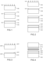
- the first part 100 and the second part 200 are then assembled ( figure 4 ).
- the solder 30 (also called filler material or soldering alloy) is advantageously a non-active solder.
- the solder is a tin solder or a solder made of a tin alloy.
- the tin alloy is chosen from SnIn, SnAg (96.5Sn-3.5Ag) and SnAgCu (96.5%Sn 3%Ag 0.5%Cu).
- the solder 30 is positioned between the two parts 100, 200 to be assembled, and more particularly between the two layers of gold 120, 210 (step iii).
- step iv After heating (step iv) and cooling (step v), an assembly with good mechanical properties is obtained.
- the parts 100, 200 are assembled by a brazing joint free of cracks.
- These implants can, for example, have brazing surfaces of the order of 20 cm2 .
- the metal part was machined into a 20 mm long and 10 mm diameter rod. It is made of Co base alloy (UNS R30008) whose composition is given in the following table: Element % by mass Co 39.0 to 42.0 Cr 18.5 to 21.5 Fe base Neither 15.0 to 18.0 Mo 6.5 to 7.5 Mn 1.0 to 2.0
- the carbon part is a POCO graphite disc coated with PyC pyrolytic carbon ( ⁇ 200 ⁇ m) 21 mm in diameter and 3 mm in height.
- Solder is a tin-based alloy SnAg. Its composition is 96.5Sn-3.5Ag (by mass), its melting point is close to that of tin (232°C).
- Such an alloy is, for example, marketed in the form of a ribbon of different thicknesses by the Indium Corporation under the trade name Indalloy-121. In these examples, the ribbon has a thickness of 100 ⁇ m.
- the carbon and metal parts are cleaned in an ultrasonic bath with acetone then ethanol and then dried with compressed air.
- the parts are then covered with metal masks (preferably stainless steel) to limit the metallization area to the assembly surface.
- metal masks preferably stainless steel
- the parts covered by the masks are positioned in the enclosure of a PVD machine, then the system is pumped up to 5 ⁇ 10 -7 mbar.
- the parts are then treated in the machine enclosure by Ar plasma in order to thoroughly clean their surfaces and form an active surface in order to improve the adhesion of the subsequent metal deposit (50W, 120 s). Then the parts are metallized.
- Example 1 Metallization of a G/PyC part by Ti/Au (figure 1):
- a 500 nm active element (Ti) bonding layer 110 is deposited on the active surface 101 of the part 1000 at a speed of 0.3 nm/s in the PVD enclosure.
- Non-active element (Au) coating layer 120 is deposited to protect the Ti thin film from oxidation and improve wetting.
- Example 2 Metallization of a G/PyC part by Ti/W/Au (figure 2):
- a 30 nm Ti bonding layer 110 is deposited on the active surface 101 of the part 100 at a speed of 0.3 nm/s in the PVD enclosure.
- a 100 nm thick W barrier layer 130 is deposited to block the diffusion and dissolution of the bonding layer 110 in the solder. This barrier layer 130 prevents the dissolution of the active element layer.
- a final layer 120 in non-active element (Au) of 100 nm thickness is made to protect the deposit from oxidation and improve wetting.
- the 200 pieces are made of CoCr.
- a 100 nm thick non-active element (Au) 210 layer is deposited to improve low temperature wetting.
- the 100 metallized G/PyC parts and the 200 metallized CoCr parts are assembled without additional cleaning.
- a 30 solder in sheet or ribbon form is cut with a die cutter and cleaned in an ultrasonic bath with acetone and then ethanol.
- the 30 solder is then positioned on the 100 carbon part ( figure 5 ), then the metal part 200 is brought into contact with the solder 30.
- the assembly is held in a tool ( figure 6 ), then placed in a secondary vacuum furnace.
- a mass is added to apply pressure (typically 15 to 20 g/cm 2 ) to the area to be brazed.
- the assembly is heated to a holding temperature, higher than the melting point of the solder (350°C, in this case) for a holding time of a few tens of minutes (10 to 15 min).
- the assemblies thus obtained by brazing are subjected to various mechanical torsion tests.
- the tests were carried out at room temperature (typically 20 to 25°C) with an electromechanical traction machine marketed by MTS Systems Corporation.
- the rotation of the mandrel is actuated by the movement of the crosshead (0.5 mm/min).
- the maximum tangential stresses (at failure) are calculated by the following formula: with F is the maximum force applied; R is the radius of the torsion axis and C the radius of the torsion pin.
- the metallization of the carbon part with the Ti/Au deposit ensures better mechanical strength due to excellent adhesion of the braze to the Ti layer.
- the fracture occurs in the braze with values corresponding to the strength of the braze itself.
- the maximum tangential stresses (at rupture) are greater than or equal to 22.8 MPa.
- the rupture is essentially adhesive and occurs at the braze/W layer interface.
Landscapes
- Engineering & Computer Science (AREA)
- Mechanical Engineering (AREA)
- Chemical & Material Sciences (AREA)
- Materials Engineering (AREA)
- Ceramic Products (AREA)
Claims (10)
- Verfahren zum Zusammenfügen eines ersten Bauteils (100) und eines zweiten Bauteils (200) durch Verlöten, umfassend die folgenden Schritte:i) Vorbereiten eines ersten Bauteils (100) aus Kohlenstoff, auf Titanbasis, auf Nickelbasis oder aus einer CoCr-Legierung,ii) Vorbereiten eines zweiten Bauteils (200) aus Kohlenstoff, auf Titanbasis, auf Nickelbasis oder aus einer CoCr-Legierung,iii) Inkontaktbringen eines Zusatzmaterials (300) mit dem ersten Bauteil (100) und mit dem zweiten Bauteil (200),iv) Erhitzen der in Schritt iii) erhaltenen Anordnung,v) Abkühlen der Anordnung, um eine Lötverbindung zwischen dem ersten Bauteil (100) und dem zweiten Bauteil (200) zu bilden, wodurch die Bauteile zusammengefügt werden,dadurch gekennzeichnet, dass das Vorbereiten des ersten Bauteils (100) während des Schritts i) und schließlich des zweiten Bauteils (200) während des Schritts ii) gemäß den folgenden Teilschritten a) bis d) durchgeführt wird:a) Bereitstellen des ersten Bauteils (100) aus Kohlenstoff, auf Titanbasis, auf Nickelbasis oder aus einer CoCr-Legierung,b) Durchführen einer Plasmabehandlung mit einem neutralen Gas am ersten Bauteil (100), wodurch das Bauteil gereinigt und eine Arbeitsoberfläche (101) auf dem Bauteil gebildet wird,c) Abscheiden einer ersten Schicht (110), die ein aktives Element umfasst, über der Arbeitsoberfläche (101) des ersten Bauteils (100), wobei das aktive Element ein karbidbildendes Element ist,d) Abscheiden einer zweiten Schicht (120) aus Gold über der ersten Schicht (110), wodurch die erste Schicht (110) vor Oxidation geschützt wird und eine gute Benetzung gewährleistet wird, unddass das Erhitzen in Schritt iv) bis zu einer Zusammenfügungstemperatur, die höher als die Schmelztemperatur des Zusatzmaterials (300) ist, durchgeführt wird, um das Zusatzmaterial zu schmelzen und die Zusammenfügungstemperatur für einen Haltezeitraum aufrechtzuerhalten, wobei die Zusammenfügungstemperatur weniger als 450°C beträgt.
- Verfahren nach Anspruch 1, dadurch gekennzeichnet, dass das aktive Element Ti, Cr oder Zr ist.
- Verfahren nach einem der Ansprüche 1 und 2, dadurch gekennzeichnet, dass die erste Schicht (110) eine Dicke von 300 µm bis 500 µm aufweist.
- Verfahren nach einem der Ansprüche 1 und 2, dadurch gekennzeichnet, dass das Verfahren einen Schritt e) zwischen Schritt c) und Schritt d) enthält, während dem eine dritte Schicht (130) eines nicht aktiven Elements, vorzugsweise W oder Nb, abgeschieden wird.
- Verfahren nach dem vorhergehenden Anspruch, dadurch gekennzeichnet, dass die erste Schicht (110) eine Dicke von 30 bis 50 nm aufweist und die dritte Schicht (130) eine Dicke von 100 bis 500 nm aufweist.
- Verfahren nach einem der Ansprüche 1 und 2, dadurch gekennzeichnet, dass die erste Schicht auch ein nicht aktives Element, vorzugsweise W oder Nb, umfasst, das gleichzeitig mit dem aktiven Element während des Schritts c) abgeschieden wird.
- Verfahren nach Anspruch 4, dadurch gekennzeichnet, dass die dritte Schicht (130) eine Dicke von 50 bis 100 nm aufweist.
- Verfahren nach einem der vorhergehenden Ansprüche, dadurch gekennzeichnet, dass das Zusatzmaterial (300) Zinn oder eine Legierung auf Zinnbasis wie SnAg, SnCu oder Snln ist.
- Verfahren nach Anspruch 8, dadurch gekennzeichnet, dass die Zusammenfügungstemperatur zwischen 250°C und 320°C beträgt.
- Verfahren nach einem der vorhergehenden Ansprüche, dadurch gekennzeichnet, dass das erste Bauteil (100) ein mit pyrolytischem Kohlenstoff bedecktes Graphitsubstrat ist und das zweite Bauteil (200) aus einer CoCr-Legierung besteht.
Applications Claiming Priority (2)
| Application Number | Priority Date | Filing Date | Title |
|---|---|---|---|
| FR2100219A FR3118721B1 (fr) | 2021-01-11 | 2021-01-11 | Procede de preparation de la surface d’une piece et procede d’assemblage par brasage direct d’une piece ainsi preparee |
| PCT/FR2022/050053 WO2022148941A1 (fr) | 2021-01-11 | 2022-01-10 | Procede d'assemblage par brasage direct d'une première pièce et d'une deuxième pièce, incluant des étapes de préparation de la surface d'au moins une des pièces |
Publications (2)
| Publication Number | Publication Date |
|---|---|
| EP4274704A1 EP4274704A1 (de) | 2023-11-15 |
| EP4274704B1 true EP4274704B1 (de) | 2025-03-05 |
Family
ID=75690379
Family Applications (1)
| Application Number | Title | Priority Date | Filing Date |
|---|---|---|---|
| EP22702754.7A Active EP4274704B1 (de) | 2021-01-11 | 2022-01-10 | Verfahren zum verbinden eines ersten teils und eines zweiten teils durch direkthartlöten, einschliesslich stufen zur vorbereitung der oberfläche von mindestens einem der teile |
Country Status (4)
| Country | Link |
|---|---|
| US (1) | US12472574B2 (de) |
| EP (1) | EP4274704B1 (de) |
| FR (1) | FR3118721B1 (de) |
| WO (1) | WO2022148941A1 (de) |
Families Citing this family (3)
| Publication number | Priority date | Publication date | Assignee | Title |
|---|---|---|---|---|
| FR3118721B1 (fr) * | 2021-01-11 | 2023-05-12 | Commissariat Energie Atomique | Procede de preparation de la surface d’une piece et procede d’assemblage par brasage direct d’une piece ainsi preparee |
| WO2022211775A1 (en) * | 2021-03-29 | 2022-10-06 | Hewlett-Packard Development Company, L.P. | Manufacturing 3d printed objects |
| CN118344170B (zh) * | 2024-03-11 | 2024-11-29 | 安徽工程大学 | 一种碳化硅与散热铜板的低温连接方法 |
Family Cites Families (13)
| Publication number | Priority date | Publication date | Assignee | Title |
|---|---|---|---|---|
| GB2137131B (en) * | 1983-03-15 | 1986-06-25 | Standard Telephones Cables Ltd | Bonding semiconductive bodies |
| US4468309A (en) * | 1983-04-22 | 1984-08-28 | White Engineering Corporation | Method for resisting galling |
| US6528123B1 (en) | 2000-06-28 | 2003-03-04 | Sandia Corporation | Coating system to permit direct brazing of ceramics |
| FR2894498B1 (fr) | 2005-12-08 | 2009-07-10 | Snecma Sa | Assemblage par brasage entre une piece metallique a base de titane et une piece en materiau ceramique a base de carbure de silicium (sic) et/ou de carbone |
| GB201015379D0 (en) * | 2010-09-15 | 2010-10-27 | Element Six N V | A diamond optical component for an optical tool |
| CN103352222B (zh) * | 2013-06-24 | 2016-03-02 | 核工业西南物理研究院 | 一种用于托卡马克装置的碳基钨涂层的制备方法 |
| GB201312388D0 (en) | 2013-07-10 | 2013-08-21 | Cambridge Entpr Ltd | Materials and methods for soldering and soldered products |
| GB201322837D0 (en) * | 2013-12-23 | 2014-02-12 | Element Six Ltd | Polycrystalline chemical vapour deposited diamond tool parts and methods of fabricating mounting and using the same |
| WO2017149810A1 (ja) * | 2016-02-29 | 2017-09-08 | 三井金属鉱業株式会社 | キャリア付銅箔及びその製造方法、並びに配線層付コアレス支持体及びプリント配線板の製造方法 |
| WO2017149811A1 (ja) * | 2016-02-29 | 2017-09-08 | 三井金属鉱業株式会社 | キャリア付銅箔、並びに配線層付コアレス支持体及びプリント配線板の製造方法 |
| FR3095151B1 (fr) * | 2019-04-16 | 2021-05-14 | Commissariat Energie Atomique | Procede d’assemblage d’une piece en carbone et d’une piece metallique par brasage |
| TWI828988B (zh) * | 2020-06-26 | 2024-01-11 | 日商日本特殊陶業股份有限公司 | 接合體及靜電夾頭 |
| FR3118721B1 (fr) * | 2021-01-11 | 2023-05-12 | Commissariat Energie Atomique | Procede de preparation de la surface d’une piece et procede d’assemblage par brasage direct d’une piece ainsi preparee |
-
2021
- 2021-01-11 FR FR2100219A patent/FR3118721B1/fr active Active
-
2022
- 2022-01-10 WO PCT/FR2022/050053 patent/WO2022148941A1/fr not_active Ceased
- 2022-01-10 EP EP22702754.7A patent/EP4274704B1/de active Active
- 2022-01-10 US US18/260,803 patent/US12472574B2/en active Active
Also Published As
| Publication number | Publication date |
|---|---|
| US20240075546A1 (en) | 2024-03-07 |
| US12472574B2 (en) | 2025-11-18 |
| FR3118721A1 (fr) | 2022-07-15 |
| FR3118721B1 (fr) | 2023-05-12 |
| EP4274704A1 (de) | 2023-11-15 |
| WO2022148941A1 (fr) | 2022-07-14 |
Similar Documents
| Publication | Publication Date | Title |
|---|---|---|
| EP4274704B1 (de) | Verfahren zum verbinden eines ersten teils und eines zweiten teils durch direkthartlöten, einschliesslich stufen zur vorbereitung der oberfläche von mindestens einem der teile | |
| EP1140416B1 (de) | Hartlötzusammensetzung und verfahren zum hartlöten von materialien auf aluminiumoxyd-basis mit dieser zusammensetzung | |
| EP1440045B1 (de) | Verfahren zum metallisieren und/oder löten oxidkeramischer bauteile mittels einer diese nicht benetzenden siliziumlegierung | |
| EP1966107B1 (de) | Gelötete verbindung zwischen einem metallteil auf titanbasis und einem keramischen teil auf basis von siliciumcarbid (sic) und/oder kohlenstoff | |
| EP0904256A1 (de) | Verfahren zur zusammenfügung von werkstoffteilen auf basis von siliciumcarbid mit hilfe einer dicken verbindungsschicht durch feuerfeste hartlötung und so erhaltene dicke feuerfeste verbindungsschicht | |
| CA2432650C (fr) | Procede de fabrication d'un produit plaque comportant une piece support en acier et un revetement metallique anti-corrosion | |
| EP0904881A1 (de) | Verbund- oder Auftragsdiffusionlötsverfahren von aus Titanaluminid hergestellten Werkstücken | |
| EP1499435B1 (de) | Verfahren zum herstellen eines elementes einer chemischen vorrichtung enthaltend ein metallisches haltewerkstück und metallische antikorrosionbeschichtung | |
| US6315188B1 (en) | Surface preparation for high purity alumina ceramics enabling direct brazing in hydrogen atmospheres | |
| FR3095151A1 (fr) | Procede d’assemblage d’une piece en carbone et d’une piece metallique par brasage | |
| JP2003112269A (ja) | ベリリウムと銅または銅合金の接合体の製造方法およびその接合体 | |
| JPH11285859A (ja) | ベリリウムと銅合金のhip接合体の製造方法およびhip接合体 | |
| WO2006095093A1 (fr) | Plaques en acier revetues de zirconium et elements de dispositifs chimiques realises avec de telles plaques | |
| JP4615746B2 (ja) | スパッタリング用チタンターゲット組立て体及びその製造方法 | |
| US20040134776A1 (en) | Assemblies comprising molybdenum and aluminum; and methods of utilizing interlayers in forming target/backing plate assemblies | |
| JPH0446070A (ja) | 金属部材とセラミックス或はサーメット部材の接合方法 | |
| EP2263820A1 (de) | Hartlötverfahren mit einem reaktiven Lotmaterial, sowie dadurch hergestellter vakuumdichter Behälter | |
| EP4197691A1 (de) | Verfahren zum verbinden eines zirkonoxidteils mit einem titanelement | |
| JPH0464795B2 (de) | ||
| JP3681824B2 (ja) | セラミックスの接合体およびセラミックスの接合方法 | |
| JP4151859B2 (ja) | スパッタリング用ターゲット板の接合方法 | |
| US20010048020A1 (en) | Welding process for ti material and cu material, and a backing plate for a sputtering target | |
| FR3095150A1 (fr) | Procede d’assemblage d’une piece en carbone et d’une piece metallique en deux etapes | |
| JPH0450107B2 (de) | ||
| JP2597105B2 (ja) | 銅部材表面硬化方法 |
Legal Events
| Date | Code | Title | Description |
|---|---|---|---|
| STAA | Information on the status of an ep patent application or granted ep patent |
Free format text: STATUS: UNKNOWN |
|
| STAA | Information on the status of an ep patent application or granted ep patent |
Free format text: STATUS: THE INTERNATIONAL PUBLICATION HAS BEEN MADE |
|
| PUAI | Public reference made under article 153(3) epc to a published international application that has entered the european phase |
Free format text: ORIGINAL CODE: 0009012 |
|
| STAA | Information on the status of an ep patent application or granted ep patent |
Free format text: STATUS: REQUEST FOR EXAMINATION WAS MADE |
|
| 17P | Request for examination filed |
Effective date: 20230705 |
|
| AK | Designated contracting states |
Kind code of ref document: A1 Designated state(s): AL AT BE BG CH CY CZ DE DK EE ES FI FR GB GR HR HU IE IS IT LI LT LU LV MC MK MT NL NO PL PT RO RS SE SI SK SM TR |
|
| DAV | Request for validation of the european patent (deleted) | ||
| DAX | Request for extension of the european patent (deleted) | ||
| GRAP | Despatch of communication of intention to grant a patent |
Free format text: ORIGINAL CODE: EPIDOSNIGR1 |
|
| STAA | Information on the status of an ep patent application or granted ep patent |
Free format text: STATUS: GRANT OF PATENT IS INTENDED |
|
| INTG | Intention to grant announced |
Effective date: 20240826 |
|
| RAP3 | Party data changed (applicant data changed or rights of an application transferred) |
Owner name: COMMISSARIAT A L'ENERGIE ATOMIQUE ET AUX ENERGIESALTERNATIVES |
|
| GRAS | Grant fee paid |
Free format text: ORIGINAL CODE: EPIDOSNIGR3 |
|
| GRAA | (expected) grant |
Free format text: ORIGINAL CODE: 0009210 |
|
| STAA | Information on the status of an ep patent application or granted ep patent |
Free format text: STATUS: THE PATENT HAS BEEN GRANTED |
|
| AK | Designated contracting states |
Kind code of ref document: B1 Designated state(s): AL AT BE BG CH CY CZ DE DK EE ES FI FR GB GR HR HU IE IS IT LI LT LU LV MC MK MT NL NO PL PT RO RS SE SI SK SM TR |
|
| REG | Reference to a national code |
Ref country code: GB Ref legal event code: FG4D Free format text: NOT ENGLISH |
|
| REG | Reference to a national code |
Ref country code: CH Ref legal event code: EP |
|
| REG | Reference to a national code |
Ref country code: DE Ref legal event code: R096 Ref document number: 602022011428 Country of ref document: DE |
|
| REG | Reference to a national code |
Ref country code: IE Ref legal event code: FG4D Free format text: LANGUAGE OF EP DOCUMENT: FRENCH |
|
| PG25 | Lapsed in a contracting state [announced via postgrant information from national office to epo] |
Ref country code: RS Free format text: LAPSE BECAUSE OF FAILURE TO SUBMIT A TRANSLATION OF THE DESCRIPTION OR TO PAY THE FEE WITHIN THE PRESCRIBED TIME-LIMIT Effective date: 20250605 |
|
| PG25 | Lapsed in a contracting state [announced via postgrant information from national office to epo] |
Ref country code: FI Free format text: LAPSE BECAUSE OF FAILURE TO SUBMIT A TRANSLATION OF THE DESCRIPTION OR TO PAY THE FEE WITHIN THE PRESCRIBED TIME-LIMIT Effective date: 20250305 |
|
| REG | Reference to a national code |
Ref country code: NL Ref legal event code: MP Effective date: 20250305 |
|
| PG25 | Lapsed in a contracting state [announced via postgrant information from national office to epo] |
Ref country code: ES Free format text: LAPSE BECAUSE OF FAILURE TO SUBMIT A TRANSLATION OF THE DESCRIPTION OR TO PAY THE FEE WITHIN THE PRESCRIBED TIME-LIMIT Effective date: 20250305 |
|
| REG | Reference to a national code |
Ref country code: LT Ref legal event code: MG9D |
|
| PG25 | Lapsed in a contracting state [announced via postgrant information from national office to epo] |
Ref country code: NO Free format text: LAPSE BECAUSE OF FAILURE TO SUBMIT A TRANSLATION OF THE DESCRIPTION OR TO PAY THE FEE WITHIN THE PRESCRIBED TIME-LIMIT Effective date: 20250605 |
|
| PG25 | Lapsed in a contracting state [announced via postgrant information from national office to epo] |
Ref country code: HR Free format text: LAPSE BECAUSE OF FAILURE TO SUBMIT A TRANSLATION OF THE DESCRIPTION OR TO PAY THE FEE WITHIN THE PRESCRIBED TIME-LIMIT Effective date: 20250305 |
|
| PG25 | Lapsed in a contracting state [announced via postgrant information from national office to epo] |
Ref country code: LV Free format text: LAPSE BECAUSE OF FAILURE TO SUBMIT A TRANSLATION OF THE DESCRIPTION OR TO PAY THE FEE WITHIN THE PRESCRIBED TIME-LIMIT Effective date: 20250305 |
|
| PG25 | Lapsed in a contracting state [announced via postgrant information from national office to epo] |
Ref country code: BG Free format text: LAPSE BECAUSE OF FAILURE TO SUBMIT A TRANSLATION OF THE DESCRIPTION OR TO PAY THE FEE WITHIN THE PRESCRIBED TIME-LIMIT Effective date: 20250305 Ref country code: GR Free format text: LAPSE BECAUSE OF FAILURE TO SUBMIT A TRANSLATION OF THE DESCRIPTION OR TO PAY THE FEE WITHIN THE PRESCRIBED TIME-LIMIT Effective date: 20250606 |
|
| REG | Reference to a national code |
Ref country code: AT Ref legal event code: MK05 Ref document number: 1772491 Country of ref document: AT Kind code of ref document: T Effective date: 20250305 |
|
| PG25 | Lapsed in a contracting state [announced via postgrant information from national office to epo] |
Ref country code: NL Free format text: LAPSE BECAUSE OF FAILURE TO SUBMIT A TRANSLATION OF THE DESCRIPTION OR TO PAY THE FEE WITHIN THE PRESCRIBED TIME-LIMIT Effective date: 20250305 |
|
| PG25 | Lapsed in a contracting state [announced via postgrant information from national office to epo] |
Ref country code: SE Free format text: LAPSE BECAUSE OF FAILURE TO SUBMIT A TRANSLATION OF THE DESCRIPTION OR TO PAY THE FEE WITHIN THE PRESCRIBED TIME-LIMIT Effective date: 20250305 |
|
| PG25 | Lapsed in a contracting state [announced via postgrant information from national office to epo] |
Ref country code: SM Free format text: LAPSE BECAUSE OF FAILURE TO SUBMIT A TRANSLATION OF THE DESCRIPTION OR TO PAY THE FEE WITHIN THE PRESCRIBED TIME-LIMIT Effective date: 20250305 |
|
| PG25 | Lapsed in a contracting state [announced via postgrant information from national office to epo] |
Ref country code: PT Free format text: LAPSE BECAUSE OF FAILURE TO SUBMIT A TRANSLATION OF THE DESCRIPTION OR TO PAY THE FEE WITHIN THE PRESCRIBED TIME-LIMIT Effective date: 20250707 |
|
| PG25 | Lapsed in a contracting state [announced via postgrant information from national office to epo] |
Ref country code: IT Free format text: LAPSE BECAUSE OF FAILURE TO SUBMIT A TRANSLATION OF THE DESCRIPTION OR TO PAY THE FEE WITHIN THE PRESCRIBED TIME-LIMIT Effective date: 20250305 Ref country code: PL Free format text: LAPSE BECAUSE OF FAILURE TO SUBMIT A TRANSLATION OF THE DESCRIPTION OR TO PAY THE FEE WITHIN THE PRESCRIBED TIME-LIMIT Effective date: 20250305 |
|
| PG25 | Lapsed in a contracting state [announced via postgrant information from national office to epo] |
Ref country code: AT Free format text: LAPSE BECAUSE OF FAILURE TO SUBMIT A TRANSLATION OF THE DESCRIPTION OR TO PAY THE FEE WITHIN THE PRESCRIBED TIME-LIMIT Effective date: 20250305 |
|
| PG25 | Lapsed in a contracting state [announced via postgrant information from national office to epo] |
Ref country code: EE Free format text: LAPSE BECAUSE OF FAILURE TO SUBMIT A TRANSLATION OF THE DESCRIPTION OR TO PAY THE FEE WITHIN THE PRESCRIBED TIME-LIMIT Effective date: 20250305 Ref country code: CZ Free format text: LAPSE BECAUSE OF FAILURE TO SUBMIT A TRANSLATION OF THE DESCRIPTION OR TO PAY THE FEE WITHIN THE PRESCRIBED TIME-LIMIT Effective date: 20250305 |
|
| PG25 | Lapsed in a contracting state [announced via postgrant information from national office to epo] |
Ref country code: RO Free format text: LAPSE BECAUSE OF FAILURE TO SUBMIT A TRANSLATION OF THE DESCRIPTION OR TO PAY THE FEE WITHIN THE PRESCRIBED TIME-LIMIT Effective date: 20250305 |
|
| PG25 | Lapsed in a contracting state [announced via postgrant information from national office to epo] |
Ref country code: SK Free format text: LAPSE BECAUSE OF FAILURE TO SUBMIT A TRANSLATION OF THE DESCRIPTION OR TO PAY THE FEE WITHIN THE PRESCRIBED TIME-LIMIT Effective date: 20250305 |
|
| PG25 | Lapsed in a contracting state [announced via postgrant information from national office to epo] |
Ref country code: IS Free format text: LAPSE BECAUSE OF FAILURE TO SUBMIT A TRANSLATION OF THE DESCRIPTION OR TO PAY THE FEE WITHIN THE PRESCRIBED TIME-LIMIT Effective date: 20250705 |
|
| REG | Reference to a national code |
Ref country code: DE Ref legal event code: R097 Ref document number: 602022011428 Country of ref document: DE |
|
| PLBE | No opposition filed within time limit |
Free format text: ORIGINAL CODE: 0009261 |
|
| STAA | Information on the status of an ep patent application or granted ep patent |
Free format text: STATUS: NO OPPOSITION FILED WITHIN TIME LIMIT |
|
| PG25 | Lapsed in a contracting state [announced via postgrant information from national office to epo] |
Ref country code: DK Free format text: LAPSE BECAUSE OF FAILURE TO SUBMIT A TRANSLATION OF THE DESCRIPTION OR TO PAY THE FEE WITHIN THE PRESCRIBED TIME-LIMIT Effective date: 20250305 |
|
| REG | Reference to a national code |
Ref country code: CH Ref legal event code: L10 Free format text: ST27 STATUS EVENT CODE: U-0-0-L10-L00 (AS PROVIDED BY THE NATIONAL OFFICE) Effective date: 20260114 |
|
| REG | Reference to a national code |
Ref country code: CH Ref legal event code: U11 Free format text: ST27 STATUS EVENT CODE: U-0-0-U10-U11 (AS PROVIDED BY THE NATIONAL OFFICE) Effective date: 20260201 |
|
| 26N | No opposition filed |
Effective date: 20251208 |
|
| PGFP | Annual fee paid to national office [announced via postgrant information from national office to epo] |
Ref country code: GB Payment date: 20260121 Year of fee payment: 5 |
|
| PGFP | Annual fee paid to national office [announced via postgrant information from national office to epo] |
Ref country code: DE Payment date: 20260120 Year of fee payment: 5 |
|
| PGFP | Annual fee paid to national office [announced via postgrant information from national office to epo] |
Ref country code: FR Payment date: 20260128 Year of fee payment: 5 |
|
| PGFP | Annual fee paid to national office [announced via postgrant information from national office to epo] |
Ref country code: CH Payment date: 20260201 Year of fee payment: 5 |