EP4294155A2 - Dispositif d'affichage à diodes électroluminescentes organiques - Google Patents
Dispositif d'affichage à diodes électroluminescentes organiques Download PDFInfo
- Publication number
- EP4294155A2 EP4294155A2 EP23205018.7A EP23205018A EP4294155A2 EP 4294155 A2 EP4294155 A2 EP 4294155A2 EP 23205018 A EP23205018 A EP 23205018A EP 4294155 A2 EP4294155 A2 EP 4294155A2
- Authority
- EP
- European Patent Office
- Prior art keywords
- layer
- display device
- spacers
- disposed
- red
- Prior art date
- Legal status (The legal status is an assumption and is not a legal conclusion. Google has not performed a legal analysis and makes no representation as to the accuracy of the status listed.)
- Pending
Links
Images








Classifications
-
- H—ELECTRICITY
- H10—SEMICONDUCTOR DEVICES; ELECTRIC SOLID-STATE DEVICES NOT OTHERWISE PROVIDED FOR
- H10K—ORGANIC ELECTRIC SOLID-STATE DEVICES
- H10K59/00—Integrated devices, or assemblies of multiple devices, comprising at least one organic light-emitting element covered by group H10K50/00
- H10K59/80—Constructional details
- H10K59/87—Passivation; Containers; Encapsulations
- H10K59/871—Self-supporting sealing arrangements
- H10K59/8723—Vertical spacers, e.g. arranged between the sealing arrangement and the OLED
-
- H—ELECTRICITY
- H10—SEMICONDUCTOR DEVICES; ELECTRIC SOLID-STATE DEVICES NOT OTHERWISE PROVIDED FOR
- H10K—ORGANIC ELECTRIC SOLID-STATE DEVICES
- H10K59/00—Integrated devices, or assemblies of multiple devices, comprising at least one organic light-emitting element covered by group H10K50/00
- H10K59/30—Devices specially adapted for multicolour light emission
- H10K59/35—Devices specially adapted for multicolour light emission comprising red-green-blue [RGB] subpixels
- H10K59/352—Devices specially adapted for multicolour light emission comprising red-green-blue [RGB] subpixels the areas of the RGB subpixels being different
-
- H—ELECTRICITY
- H10—SEMICONDUCTOR DEVICES; ELECTRIC SOLID-STATE DEVICES NOT OTHERWISE PROVIDED FOR
- H10K—ORGANIC ELECTRIC SOLID-STATE DEVICES
- H10K50/00—Organic light-emitting devices
- H10K50/80—Constructional details
- H10K50/805—Electrodes
- H10K50/82—Cathodes
- H10K50/822—Cathodes characterised by their shape
-
- H—ELECTRICITY
- H10—SEMICONDUCTOR DEVICES; ELECTRIC SOLID-STATE DEVICES NOT OTHERWISE PROVIDED FOR
- H10K—ORGANIC ELECTRIC SOLID-STATE DEVICES
- H10K59/00—Integrated devices, or assemblies of multiple devices, comprising at least one organic light-emitting element covered by group H10K50/00
- H10K59/10—OLED displays
- H10K59/12—Active-matrix OLED [AMOLED] displays
- H10K59/122—Pixel-defining structures or layers, e.g. banks
-
- H—ELECTRICITY
- H10—SEMICONDUCTOR DEVICES; ELECTRIC SOLID-STATE DEVICES NOT OTHERWISE PROVIDED FOR
- H10K—ORGANIC ELECTRIC SOLID-STATE DEVICES
- H10K59/00—Integrated devices, or assemblies of multiple devices, comprising at least one organic light-emitting element covered by group H10K50/00
- H10K59/10—OLED displays
- H10K59/12—Active-matrix OLED [AMOLED] displays
- H10K59/123—Connection of the pixel electrodes to the thin film transistors [TFT]
-
- H—ELECTRICITY
- H10—SEMICONDUCTOR DEVICES; ELECTRIC SOLID-STATE DEVICES NOT OTHERWISE PROVIDED FOR
- H10K—ORGANIC ELECTRIC SOLID-STATE DEVICES
- H10K59/00—Integrated devices, or assemblies of multiple devices, comprising at least one organic light-emitting element covered by group H10K50/00
- H10K59/30—Devices specially adapted for multicolour light emission
- H10K59/35—Devices specially adapted for multicolour light emission comprising red-green-blue [RGB] subpixels
-
- H—ELECTRICITY
- H10—SEMICONDUCTOR DEVICES; ELECTRIC SOLID-STATE DEVICES NOT OTHERWISE PROVIDED FOR
- H10K—ORGANIC ELECTRIC SOLID-STATE DEVICES
- H10K59/00—Integrated devices, or assemblies of multiple devices, comprising at least one organic light-emitting element covered by group H10K50/00
- H10K59/30—Devices specially adapted for multicolour light emission
- H10K59/35—Devices specially adapted for multicolour light emission comprising red-green-blue [RGB] subpixels
- H10K59/353—Devices specially adapted for multicolour light emission comprising red-green-blue [RGB] subpixels characterised by the geometrical arrangement of the RGB subpixels
-
- H—ELECTRICITY
- H10—SEMICONDUCTOR DEVICES; ELECTRIC SOLID-STATE DEVICES NOT OTHERWISE PROVIDED FOR
- H10K—ORGANIC ELECTRIC SOLID-STATE DEVICES
- H10K59/00—Integrated devices, or assemblies of multiple devices, comprising at least one organic light-emitting element covered by group H10K50/00
- H10K59/80—Constructional details
- H10K59/805—Electrodes
- H10K59/8052—Cathodes
- H10K59/80521—Cathodes characterised by their shape
Definitions
- the present disclosure is directed to an organic light emitting diode display device that substantially obviate one or more of the problems due to limitations and disadvantages of the related art.
- the element In construing an element, the element is construed as including an error or tolerance range even where no explicit description of such an error or tolerance range.
- FIG. 1 is a view showing an organic light emitting diode display device according to a first embodiment of the present disclosure.
- an organic light emitting diode (OLED) display device 100 includes an image processing unit 101, a timing controlling unit 102, a gate driving unit 103, a data driving unit 104, a power supplying unit 106 and a display panel PNL.
- the image processing unit 101 outputs an image data and a plurality of timing signals for driving various units.
- the plurality of timing signals outputted from the image processing unit 101 may include a data enable signal, a horizontal synchronization signal, a vertical synchronization signal and a clock signal.
- the timing controlling unit 102 receives the image data and the plurality of timing signals from the image processing unit 101.
- the timing controlling unit 102 generates and outputs a gate control signal GDC for controlling an operation timing of the gate driving unit 103 and a data control signal DDC for controlling an operation timing of the data driving unit 104 based on the plurality of timing signals supplied from the image processing unit 101.
- the gate driving unit 103 outputs a scan signal to the display panel PNL in response to the gate control signal supplied from the timing controlling unit 102.
- the gate driving unit 103 outputs the scan signal through a plurality of gate lines GL1 to GLm.
- the gate driving unit 103 may be formed as an integrated circuit (IC), it is not limited thereto.
- the gate driving unit 103 may have a gate-in-panel (GIP) structure where a thin film transistor are formed on a substrate of the OLED display device 100.
- the GIP structure may include a plurality of circuits such as a shift register and a level shifter.
- the data driving unit 104 outputs a data voltage to the display panel PNL in response to the data control signal DDC supplied from the timing controlling unit 102.
- the data driving unit 104 performs a sampling and a latch of a data signal DATA of a digital type supplied from the timing controlling unit 102 and coverts the data signal DATA into the data voltage of an analog type based on a gamma voltage.
- the data driving unit 104 outputs the data voltage through a plurality of data lines DL1 to DLn.
- the data driving unit 104 may be mounted on the display panel PNL as an integrated circuit (IC) or may be laminated directly on the display panel PNL as various patterns and layers, it is not limited thereto.
- IC integrated circuit
- the power supplying unit 106 outputs and supplies a high level voltage EVDD and a low level voltage EVSS to the display panel PNL.
- the high level voltage EVDD and the low level voltage EVSS are supplied to the display panel PNL through a power line.
- the voltages outputted from the power supplying unit 106 may be transmitted to the gate driving unit 104 or the data driving unit 104 for driving the gate driving unit 104 or the data driving unit 104.
- the display panel PNL displays an image in response to the scan signal, the data voltage and the voltages supplied from the gate driving unit 103, the data driving unit 104 and the power supplying unit 106, respectively.
- the display panel PNL includes a plurality of subpixels SP for displaying an image.
- the plurality of subpixels SP includes red, green and blue subpixels or white, red, green and blue subpixels.
- the white, red, green and blue subpixels may have the same area as each other or may have different areas from each other.
- FIG. 2 is a circuit diagram showing a subpixel of a display panel PNL of an organic light emitting diode display device according to a first embodiment of the present disclosure.
- the display panel PNL of the OLED display device 100 includes a display area and a pad area, and the display area includes the plurality of subpixels SP.
- Each subpixel SP displays a single color in the OLED display device 100.
- each subpixel SP may display one of red, green, blue and white colors, and red, green, blue and white subpixels SP may be defined as a single pixel.
- the plurality of subpixels SP are disposed in a matrix on a substrate of the OLED display device 100, and a plurality of lines are disposed between the plurality of subpixels SP in the display area.
- a plurality of link lines electrically connected to the plurality of lines in the display area and supplying signals to elements of the OLED display device 100 may be disposed in the pad area.
- the plurality of link lines may include a high level voltage (Vdd) line, a data voltage (Vdata) line, a reference voltage (Vref) line and a low level voltage (Vss) line.
- each subpixel SP of the display panel PNL of the OLED display device 100 includes a switching thin film transistor (TFT) T1, a driving TFT T2, a storage capacitor Cst, a sensing TFT T3, an auxiliary TFT T4 and a light emitting diode E. Since the subpixel SP of the OLED display device 100 includes 4 TFTs and 1 capacitor, the subpixel SP may be referred to as a 4T1C structure. However, a structure of the subpixel SP of the OLED display device 100 is not limited thereto.
- Each of 4 TFTs in the subpixel SP includes a semiconductor layer, a gate electrode, a source electrode and a drain electrode, and may have a positive type or a negative type.
- FIG. 2 exemplarily shows a negative type thin film transistor.
- the switching TFT T1 includes a drain electrode connected to the data line, a source electrode connected to a first node N1 and a gate electrode connected to the gate line.
- the switching TFT T1 is turned on according to the gate voltage Vg applied to the gate line from the gate driving unit and transmits the data voltage Vdata applied through the data line from the data driving unit to the first node N1.
- the driving TFT T2 includes a drain electrode connected to a high level voltage (Vdd) line, a source electrode connected to an anode of the light emitting diode E and a gate electrode connected to the first node N1.
- the driving TFT T2 is turned on when a voltage of the first node N1 is greater than a threshold voltage Vth and is turned off when a voltage of the first node N1 is smaller than a threshold voltage Vth.
- the driving TFT T2 transmits a driving current of the high level voltage (Vdd) line to the light emitting diode E.
- the storage capacitor Cst includes a first electrode connected to the first node N1 and a second node N2 connected to the source electrode of the driving TFT T2.
- the storage capacitor Cst keeps a voltage difference between the gate electrode and the source electrode of the driving TFT T2 constant during an emission time where the light emitting diode E emits a light so that a constant driving current can be transmitted to the light emitting diode E.
- the sensing TFT T3 includes a drain electrode connected to the source electrode of the driving TFT T2, a source electrode connected to the reference line and a gate electrode connected to a sensing line.
- the sensing TFT T3 is a thin film transistor for sensing the threshold voltage of the driving TFT T2.
- the auxiliary TFT T4 includes a drain electrode electrically connected to a cathode of the light emitting diode E, a source electrode electrically connected to the reference line and a gate electrode electrically connected to an auxiliary line.
- the auxiliary TFT T4 is turned on during an emission period to transmit the low level voltage Vss to the cathode of the light emitting diode E.
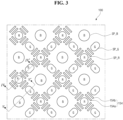
- FIG. 3 is a plan view showing an organic light emitting diode display device according to a first embodiment of the present disclosure.
- a plurality of spacers 154 each having a reversed taper shape in a cross-sectional view are disposed in a periphery of the red subpixel SP_R, while the plurality of spacers 154 are not disposed in a periphery of the green and blue subpixels SP_G and SP_B.
- a width of a top portion (top surface) is greater than a width of the bottom portion (bottom surface).
- the plurality of spacers 154 each having a bar shape in a plan view are disposed in four peripheral sides of the red subpixel SP_R to surround the red subpixel SP_R.
- the plurality of spacers 154 surrounding the red subpixel SP_R are spaced apart from each other.
- four spacers 154 are disposed in a rectangular shape and the red subpixel SP_R is disposed in the rectangular shape in FIG. 3
- the spacers 154 equal to or greater than five may be disposed in a polygonal shape or a circular shape and the red subpixel SP_R may be disposed in the polygonal shape or the circular shape in another embodiment.
- the TFT T includes a semiconductor layer 114 on a buffer layer 142 over a first substrate 110, a gate insulating layer 143 covering the semiconductor layer 114 on the buffer layer 142, a gate electrode 116 on the gate insulating layer 143, an interlayer insulating layer 144 covering the gate electrode 116 over the gate insulating layer 143 and source and drain electrodes 122 and 124 on the interlayer insulating layer 144.
- the interlayer insulating layer 144 may include an organic material such as photoacryl or may have a single layer or a multiple layer of an inorganic material such as silicon nitride (SiNx) or silicon oxide (SiOx). In addition, the interlayer insulating layer 144 may have a multiple layer of an organic layer and an inorganic layer.
- Source and drain electrodes 122 and 124 are connected to the source and drain regions 114b and 114c, respectively, of the semiconductor layer 114 through first and second contact holes 149a and 149b in the gate insulating layer 143 and the interlayer insulating layer 144.
- An electron transporting layer 136 is disposed on the emitting layer 135 between the adjacent bank layer 152, the hole transporting layer 134 over the top surface of the bank layer 152 and the hole transporting layer 134 over the side and top surfaces of the spacer 154.
- a cathode 138 is disposed on the electron transporting layer 136 between the adjacent bank layers 152, the electron transporting layer 136 over the top surface of the bank layer 152 and the electron transporting layer 136 over the top surface of the spacer 154.
- the cathode 138 is not disposed on the electron transporting layer 136 over the side surface of the spacer 154.
- the cathode 138 is disposed over the top surface of the bank layer 152 and the top surface of the spacer 154, the cathode 138 is not disposed over the side surface of the reversely tapered spacer 154.
- the cathode 138 over the top surface of the bank layer 152 and the cathode 138 over the top surface of the spacer 154 are cut due to the side surface of the reversely tapered spacer 154.
- a hole injecting layer may be disposed between the anode 132 and the hole transporting layer 134, and an electron injecting layer may be disposed on the electron transporting layer 136.
- the hole transporting layer 134 and the electron transporting layer 136 are disposed on the side and top surfaces of the spacer 154, the hole transporting layer 134 and the electron transporting layer 136 are disposed on an entire surface of the OLED display device 100.
- the cathode 138 is cut due to the spacer 154.
- a lateral leakage current is generated and is transmitted to the adjacent subpixel. Since the lateral leakage current causes an error in a current of the adjacent subpixel, a uniformity of a luminance between the subpixels is deteriorated.
- the adjacent subpixel having an off state may be turned on due to the lateral leakage current to emit a light. Specifically, since a gap distance between the subpixels is reduced in a high resolution display device, a bad influence of the lateral leakage current increases.
- the lateral leakage current flows through a common layer such as the hole transporting layer 134, the electron transporting layer 136, the hole injecting layer and the electron injecting layer to be transmitted to the adjacent subpixel.
- a transmission of the lateral leakage current to the adjacent subpixel is minimized by adjusting a current path of the lateral leakage current.
- the hole transporting layer 134 and the electron transporting layer 136 are disposed on the side and top surfaces of the spacer 154, the current path of the lateral leakage current is elongated. As a result, the lateral leakage current transmitted to the adjacent subpixel is minimized due to an increase of a length of the current path.
- the cathode 138 over a whole of the OLED display device 100 is cut in a region of the spacer 154, and an increase of a length of a current path of the low level voltage Vss is prevented.
- the current of the low level voltage Vss flows through the cathode 138.
- the increase of the length of the current path of the low level voltage Vss causes a rising of the low level voltage Vss.
- a driving voltage and a power consumption increase and a uniformity of a luminance is deteriorated due to the rising of the low level voltage Vss.
- the cathode 154 When the cathode 138 is not cut by the spacer 154, the cathode 154 extends to the side and top surfaces of the spacer 154. As a result, the current path of the low level voltage Vss is elongated and the low level voltage Vss increases.
- the cathode 138 is cut in the region of the reversely tapered spacer 154 to prevent the rising of the low level voltage Vss. Since the current path of the low level voltage Vss is prevented from being formed on the top and side surfaces of the first spacer 154a and the top and side surfaces of the second spacer 154b, the increase of the current path of the low level voltage Vss is minimized due to the spacer 154.
- the spacer 154 having a reverse taper shape is disposed on the bank layer 152.
- the current path of the lateral leakage current is elongated and the lateral leakage current to the adjacent subpixel is minimized.
- the increase of the length of the current path of the low level voltage Vss is minimized and the rising of the low level voltage Vss is minimized.
- the spacer 154 is disposed in a periphery of the red subpixel SP_R and is not disposed in a periphery of the green and blue subpixels SP_G and SP_B.
- the cathode 138 is cut in the region of the spacer 154.
- the current path is elongated as compared with a comparison example where the spacer 154 is omitted.
- a length of the current path of the low level voltage Vss increases as compared with a comparison example where the spacer 154 is omitted and the current of the low level voltage Vss is transmitted through the first current path, a property of the OLED display device 100 may be deteriorated due to the rising of the low level voltage.
- the OLED device 100 has an advantage that the lateral leakage current decreases and a disadvantage that the low level voltage increases.
- the advantage the lateral leakage current decreases is maximized and the disadvantage that that the low level voltage increases is minimized. As a result, an efficiency of the OLED display device 100 is improved.
- the red, green and blue subpixels SP_R, SP_G and SP_B a relatively small current is applied to the red subpixel SP_R and a relatively great current is applied to the green and blue subpixels SP_G and SP_B.
- the TFT T in the red subpixel SP_R has a relatively low threshold voltage and the TFT T in the green and blue subpixels SP_G and SP_B has a relatively high threshold voltage.
- the spacer 154 is disposed in the periphery of the red subpixel SP_R having a maximum influence by the lateral leakage current, and the spacer 154 is not disposed in the periphery of the green and blue subpixels SP_G and SP_B having a minimum influence by the lateral leakage current. As a result, deterioration due to the lateral leakage current is prevented.
- an encapsulation layer 160 is disposed on the cathode 136.
- the encapsulation layer 160 may include a first encapsulation layer 162 of an inorganic material, a second encapsulation layer 164 of an organic material and a third encapsulation layer 166 of an inorganic material.
- the inorganic material may include silicon nitride (SiNx) and silicon oxide (SiOx), it is not limited thereto.
- the organic material may include polyethylene terephthalate (PET), polyethylene naphthalate (PEN), polycarbonate (PC), polyimide (PI), polyethylene sulfonate (PES), polyoxymethylene (POM), polyarylate (PAR) and a mixture thereof, it is not limited thereto.
- PET polyethylene terephthalate
- PEN polyethylene naphthalate
- PC polycarbonate
- PI polyimide
- PES polyethylene sulfonate
- POM polyoxymethylene
- PAR polyarylate
- the second substrate 170 as an encapsulation cap may include a protecting film such as a polystyrene film, a polyethylene film, a polyethylene naphthalate film and a polyimide film or a glass of a thickness of about 10 ⁇ m to about 99 ⁇ m.
- a protecting film such as a polystyrene film, a polyethylene film, a polyethylene naphthalate film and a polyimide film or a glass of a thickness of about 10 ⁇ m to about 99 ⁇ m.
- the spacer 154 includes the first and second sub-spacers 154a and 154b in a first embodiment, the spacer 154 may include one sub-spacer or three or more sub-spacers in another embodiment.
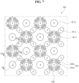
- FIG. 7 is a plan view showing an organic light emitting diode display device according to a second embodiment of the present disclosure
- FIG. 8 is a cross-sectional view taken along a line VIII-VIII' of FIG. 7
- FIG. 9 is a cross-sectional view taken along a line IX-IX' of FIG. 7 . Illustration on a part that is the same as the first embodiment will be omitted.
- an organic light emitting diode (OLED) display device 200 may include a red subpixel SP_R, a green subpixel SP_G and a blue subpixel SP_B.
- a plurality of spacers 254 each having a reversed taper shape in a cross-sectional view are disposed in a periphery of the red subpixel SP_R, while the plurality of spacers 254 are not disposed in a periphery of the green and blue subpixels SP_G and SP_B.
- a groove 256 of a predetermined width is disposed along a boundary of the red subpixel SP_R to have a closed curve (loop) shape in a periphery of the red subpixel SP_R.
- the groove 256 may be disposed between the first and second sub-spacers 254a and 254b.
- the groove 256 may be disposed inside the first sub-spacer 254a or outside the second sub-spacer 254b to surround the red subpixel SP_R.
- a thin film transistor (TFT) T is disposed on a first substrate 210, and a bank layer 252 is disposed over the TFT T.
- TFT thin film transistor
- a reversely tapered spacer 254 is disposed on the bank layer 252 between the red and green subpixels SP_R and SP_G and in a periphery of the red subpixel SP_R.
- the spacer 254 includes first and second sub-spacers 254a and 254b spaced apart from each other in a second embodiment, the spacer 254 may include one sub-spacer or three or more sub-spacers in another embodiment.
- the groove 256 is disposed in a periphery of the red subpixel SP_R on the bank layer 252.
- the groove 256 is spaced apart from the first and second sub-spacers 254a and 254b and has a predetermined width.
- a sidewall of the groove 256 may have a slanting angle equal to or smaller than about 90 degree to have a taper shape.
- the groove 256 may be disposed between the first and second sub-spacers 254a and 254b in a second embodiment, the groove 256 may be disposed outside the first and second sub-spacers 254a and 254b in another embodiment.
- the groove 256 may have one sub-groove in a second embodiment, the groove 256 may have two or more sub-grooves in another embodiment.
- a plurality of sub-grooves may be disposed between the first and second sub-spacers 254a and 254b or may be disposed outside the first and second sub-spacers 254a and 254b.
- the spacer 254 may include the same material as the bank layer 252 or may have a different material from the bank layer 252. For example, when the spacer 254 and the bank layer 252 include the same material as each other, the spacer 254 and the bank layer 252 may be formed through a single mask process. Further, the spacer 254, the bank layer 252 and the groove 256 may be formed through a single mask process.
- a hole transporting layer 234 is disposed on the anode 232 between the adjacent bank layers 252, an top surface of the bank layer 252, side and top surfaces of the spacer 254 and side and bottom surfaces of the groove 256.
- An emitting layer 235 is disposed on the hole transporting layer 234 between the adjacent bank layers 252.
- the emitting layer 235 may include a red emitting layer emitting a red colored light in the red subpixel SP_R, a green emitting layer emitting a green colored light in the green subpixel SP_G and a blue emitting layer emitting a blue colored light in the blue subpixel SP_B.
- the emitting layer 235 may include a white emitting layer emitting a white colored light in the red, green and blue subpixels SP_R, SP_G and SP_B.
- a cathode 238 is disposed on the electron transporting layer 236 between the adjacent bank layers 252, the electron transporting layer 236 over the top surface of the bank layer 252, the electron transporting layer 236 over the top surface of the spacer 254 and the electron transporting layer 236 over the side and bottom surfaces of the groove 256.
- the cathode 238 is not disposed on the electron transporting layer 236 over the side surface of the spacer 254.
- the cathode 238 is disposed over the top surface of the bank layer 252, the top surface of the spacer 254 and an inner surface of the groove 256, the cathode 238 is not disposed over the side surface of the reversely tapered spacer 254.
- the cathode 238 over the top surface of the bank layer 252 and the cathode 238 over the top surface of the spacer 254 are cut due to the side surface of the reversely tapered spacer 254.
- the hole transporting layer 234 and the electron transporting layer 236 are disposed on the side and top surfaces of the spacer 254 and the side and bottom surfaces of the groove 256, the hole transporting layer 234 and the electron transporting layer 236 are disposed on an entire surface of the OLED display device 200.
- the cathode 238 is cut due to the spacer 254.
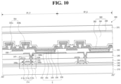
- FIGs. 10 and 11 are cross-sectional views showing an organic light emitting diode display device according to a third embodiment of the present disclosure.
- FIG. 10 corresponds to a cross-sectional view taken along a line VIII-VIII' of FIG. 7
- FIG. 11 corresponds to a cross-sectional view taken along a line IX-IX' of FIG. 7 . Illustration on a part that is the same as the first and second embodiments will be omitted.
- a thin film transistor (TFT) T an organic light emitting diode (OLED) display device 300 according to a third embodiment of the present disclosure is disposed on a first substrate 310, and a bank layer 352 is disposed over the TFT T.
- TFT thin film transistor
- OLED organic light emitting diode
- a reversely tapered spacer 354 is disposed on the bank layer 352 between red and green subpixels SP_R and SP_G and in a periphery of the red subpixel SP_R.
- the spacer 354 includes first and second sub-spacers 354a and 354b spaced apart from each other in a third embodiment, the spacer 354 may include one sub-spacer or three or more sub-spacers in another embodiment.
- a groove 356 having a closed curve (loop) shape of a predetermined width is disposed in a periphery of the red subpixel SP_R on the bank layer 352.
- the groove 356 may form a closed loop which surrounds the red subpixel.
- the groove 356 is spaced apart from the first and second sub-spacers 354a and 354b.
- a sidewall of the groove 356 may have a slanting angle equal to or greater than about 90 degree to have a reverse taper shape.
- the groove 356 may be disposed between the first and second sub-spacers 354a and 354b in a third embodiment, the groove 356 may be disposed outside the first and second sub-spacers 354a and 354b in another embodiment.
- the groove 356 may have one sub-groove in a third embodiment, the groove 356 may have two or more sub-grooves in another embodiment.
- a plurality of sub-grooves may be disposed between the first and second sub-spacers 354a and 354b or may be disposed outside the first and second sub-spacers 354a and 354b.
- An anode 332 is disposed on a passivation layer 346 between the adjacent bank layers 352 and is electrically connected to a drain electrode 324 of the TFT T through a third contact hole 349c in the passivation layer 346.
- a hole transporting layer 334 is disposed on the anode 332 between the adjacent bank layers 352, an top surface of the bank layer 352, side and top surfaces of the spacer 354 and side and bottom surfaces of the groove 356.
- An emitting layer 335 is disposed on the hole transporting layer 334 between the adjacent bank layers 352.
- the emitting layer 335 may include a red emitting layer emitting a red colored light in the red subpixel SP_R, a green emitting layer emitting a green colored light in the green subpixel SP_G and a blue emitting layer emitting a blue colored light in the blue subpixel SP_B.
- the emitting layer 335 may include a white emitting layer emitting a white colored light in the red, green and blue subpixels SP_R, SP_G and SP_B.
- An electron transporting layer 336 is disposed on the emitting layer 335 between the adjacent bank layer 352, the hole transporting layer 334 over the top surface of the bank layer 352, the hole transporting layer 334 over the side and top surfaces of the spacer 354 and the hole transporting layer 334 over the side and bottom surfaces of the groove 356.
- a cathode 338 is disposed on the electron transporting layer 336 between the adjacent bank layers 352, the electron transporting layer 336 over the top surface of the bank layer 352, the electron transporting layer 336 over the top surface of the spacer 354 and the electron transporting layer 336 over the bottom surface of the groove 356.
- the cathode 338 is not disposed on the electron transporting layer 336 over the side surface of the spacer 354 and the side surface of the groove 356.
- the cathode 338 is disposed over the top surface of the bank layer 352, the top surface of the spacer 354 and the bottom surface of the groove 356, the cathode 338 is not disposed over the side surface of the reversely tapered spacer 354 and the side surface of the reversely tapered groove 356.
- the cathode 338 over the top surface of the bank layer 352 and the cathode 338 over the top surface of the spacer 354 are cut due to the side surface of the reversely tapered spacer 354, and the cathode 338 over the top surface of the bank layer 352 and the cathode 338 over the bottom surface of the groove 356 are cut due to the side surface of the reversely tapered groove 356.
- the hole transporting layer 334 and the electron transporting layer 336 are disposed on the side and top surfaces of the spacer 354 and the side and bottom surfaces of the groove 356, the hole transporting layer 334 and the electron transporting layer 336 are disposed on an entire surface of the OLED display device 300.
- the lateral leakage current transmitted to the adjacent subpixel is reduced due to an increase of a length of the current path.
- the light emitting diode E has a one-stack structure in the first to third embodiment, the light emitting diode E may have a two-stack structure in another embodiment.
- FIG. 12 is a view showing an organic light emitting diode display device according to a fourth embodiment of the present disclosure. A part of the fourth embodiment the same as the first to third embodiments will be omitted.
- an organic light emitting diode (OLED) display device 400 may include red, green and blue subpixels SP_R, SP_G and SP_B.
- An anode 430 is disposed in each of the red, green and blue subpixels SP_R, SP_G and SP_B on a substrate 410.
- a hole injecting layer (HIL) 440 is disposed in a whole of the red, green and blue subpixels SP_R, SP_G and SP_B on the anode 430, and a first hole transporting layer (HTL) 442 is disposed in a whole of the red, green and blue subpixels SP_R, SP_G and SP_B on the HIL 440.
- HIL hole injecting layer
- HTL first hole transporting layer
- a positive type hole transporting layer instead of the HIL 440 may be disposed between the anode 430 and the first HTL 442.
- a first red emitting material layer (EML) 444R is selectively disposed in the red subpixel SP_R on the first HTL 442
- a first green EML 444G is selectively disposed in the green subpixel SP_G on the first HTL 442
- a first blue EML 444B is selectively disposed in the blue subpixel SP_B on the first HTL 442.
- the first red, green and blue EMLs 444R, 444G and 444B may adjust a length of an optical path in the red, green and blue subpixels SP_R, SP_G and SP_B to obtain a micro cavity.
- a thickness of the first green EML 444G may be greater than or equal to a thickness of the first blue EML 444B and may be smaller than or equal to a thickness of the first red EML 444R.
- a first electron transporting layer (ETL) 446 is disposed on a whole of the first red EML 444R of the red subpixel SP_R, the first green EML 444G of the green subpixel SP_G and the first blue EML 444B of the blue subpixel SP_B.
- the HIL 440, the first HTL 442, the first red, green and blue EMLs 444R, 444G and 444B and the first ETL 446 constitute a first stack ST1.
- An N type charge generation layer (CGL) 448 is disposed on the first ETL 446 in the red, green and blue subpixels SP_R, SP_G and SP_B, and a P type CGL 450 is disposed on the N type CGL 448 in the red, green and blue subpixels SP_R, SP_G and SP_B.
- the N type CGL 448 and the P type CGL 450 may generate and supply an electron and a hole.
- the N type CGL 448 may supply an electron to the first stack ST1
- the P type CGL 450 may supply a hole to a second stack ST2.
- a second HTL 452 is disposed on the P type CGL 450 in the red, green and blue subpixels SP_R, SP_Gand SP_B.
- a second red EML 454R is selectively disposed in the red subpixel SP_R on the second HTL 452
- a second green EML 454G is selectively disposed in the green subpixel SP_G on the second HTL 452
- a first blue EML 454B is selectively disposed in the blue subpixel SP_B on the second HTL 452.
- a second ETL 456 is disposed on a whole of the second red EML 454R of the red subpixel SP_R, the second green EML 454G of the green subpixel SP_G and the second blue EML 454B of the blue subpixel SP_B.
- the second HTL 452, the second red, green and blue EMLs 454R, 454G and 454B, the second ETL 456 and the EII, 458 constitute a second stack ST2.
- the anode 430, the first stack ST1, the N type CGL 448, the P type CGL 450, the second stack ST2 and the cathode 470 may constitute a light emitting diode.
- the light emitting diode E may have a three-stack structure.
- the spacer is disposed in the periphery of the red subpixel having the maximum influence by the lateral leakage current and the spacer is not disposed in the periphery of the green and blue subpixels having the minimum influence by the lateral leakage current. As a result, deterioration due to the lateral leakage current is effectively prevented.
- the spacer is disposed only in the periphery of the red subpixel having the maximum influence by the lateral leakage current, the rising of the low level voltage due to the spacer is minimized.
Landscapes
- Engineering & Computer Science (AREA)
- Microelectronics & Electronic Packaging (AREA)
- Physics & Mathematics (AREA)
- Optics & Photonics (AREA)
- Electroluminescent Light Sources (AREA)
- Devices For Indicating Variable Information By Combining Individual Elements (AREA)
Applications Claiming Priority (2)
| Application Number | Priority Date | Filing Date | Title |
|---|---|---|---|
| KR1020210191084A KR20230101185A (ko) | 2021-12-29 | 2021-12-29 | 유기전계발광 표시장치 |
| EP22208405.5A EP4207975A1 (fr) | 2021-12-29 | 2022-11-18 | Dispositif d'affichage à diodes électroluminescentes organiques |
Related Parent Applications (1)
| Application Number | Title | Priority Date | Filing Date |
|---|---|---|---|
| EP22208405.5A Division EP4207975A1 (fr) | 2021-12-29 | 2022-11-18 | Dispositif d'affichage à diodes électroluminescentes organiques |
Publications (2)
| Publication Number | Publication Date |
|---|---|
| EP4294155A2 true EP4294155A2 (fr) | 2023-12-20 |
| EP4294155A3 EP4294155A3 (fr) | 2024-02-21 |
Family
ID=84360491
Family Applications (2)
| Application Number | Title | Priority Date | Filing Date |
|---|---|---|---|
| EP22208405.5A Pending EP4207975A1 (fr) | 2021-12-29 | 2022-11-18 | Dispositif d'affichage à diodes électroluminescentes organiques |
| EP23205018.7A Pending EP4294155A3 (fr) | 2021-12-29 | 2022-11-18 | Dispositif d'affichage à diodes électroluminescentes organiques |
Family Applications Before (1)
| Application Number | Title | Priority Date | Filing Date |
|---|---|---|---|
| EP22208405.5A Pending EP4207975A1 (fr) | 2021-12-29 | 2022-11-18 | Dispositif d'affichage à diodes électroluminescentes organiques |
Country Status (6)
| Country | Link |
|---|---|
| US (1) | US20230209910A1 (fr) |
| EP (2) | EP4207975A1 (fr) |
| JP (2) | JP7510483B2 (fr) |
| KR (1) | KR20230101185A (fr) |
| CN (2) | CN116367579A (fr) |
| TW (2) | TWI881256B (fr) |
Families Citing this family (7)
| Publication number | Priority date | Publication date | Assignee | Title |
|---|---|---|---|---|
| KR20220118580A (ko) * | 2021-02-18 | 2022-08-26 | 삼성디스플레이 주식회사 | 표시 장치 및 표시 장치의 제조 방법 |
| JP7709423B2 (ja) * | 2022-04-20 | 2025-07-16 | キヤノン株式会社 | 発光装置、表示装置、光電変換装置、電子機器および移動体 |
| CN117042493A (zh) * | 2023-09-22 | 2023-11-10 | 京东方科技集团股份有限公司 | 串联式oled结构及显示面板 |
| US20250176360A1 (en) * | 2023-11-29 | 2025-05-29 | Lg Display Co., Ltd. | Display device and method for manufacturing the same |
| JP7753325B2 (ja) * | 2023-12-13 | 2025-10-14 | エルジー ディスプレイ カンパニー リミテッド | 発光表示装置 |
| JP2026039598A (ja) * | 2024-08-23 | 2026-03-09 | キヤノン株式会社 | 半導体装置、表示装置、及び光電変換装置 |
| CN119136587B (zh) * | 2024-08-30 | 2025-10-10 | 武汉华星光电半导体显示技术有限公司 | 显示面板及显示装置 |
Family Cites Families (20)
| Publication number | Priority date | Publication date | Assignee | Title |
|---|---|---|---|---|
| JP2002208489A (ja) * | 2000-11-10 | 2002-07-26 | Toyota Industries Corp | 有機エレクトロルミネッセンスディスプレイパネル及びその製造方法 |
| JP4225237B2 (ja) * | 2004-04-21 | 2009-02-18 | セイコーエプソン株式会社 | 有機el装置及び有機el装置の製造方法並びに電子機器 |
| JP5125886B2 (ja) * | 2008-08-26 | 2013-01-23 | 大日本印刷株式会社 | 有機エレクトロルミネッセンス素子およびその製造方法 |
| KR101920374B1 (ko) * | 2011-04-27 | 2018-11-20 | 가부시키가이샤 한도오따이 에네루기 켄큐쇼 | 발광 장치 및 그 제작 방법 |
| KR101933952B1 (ko) * | 2011-07-01 | 2018-12-31 | 가부시키가이샤 한도오따이 에네루기 켄큐쇼 | 발광 장치, 전자 기기 및 조명 장치 |
| KR102030799B1 (ko) * | 2013-03-11 | 2019-10-11 | 삼성디스플레이 주식회사 | 유기발광표시장치 |
| JP6136578B2 (ja) * | 2013-05-29 | 2017-05-31 | ソニー株式会社 | 表示装置および表示装置の製造方法ならびに電子機器 |
| JP6232277B2 (ja) * | 2013-12-18 | 2017-11-15 | 東京エレクトロン株式会社 | 有機el素子構造、その製造方法及び発光パネル |
| US9934723B2 (en) * | 2014-06-25 | 2018-04-03 | Lg Display Co., Ltd. | Thin film transistor substrate, display panel including the same, and method of manufacturing the same |
| KR102420453B1 (ko) * | 2015-09-09 | 2022-07-13 | 엘지디스플레이 주식회사 | 유기발광 표시장치 및 이를 적용한 차량용 조명장치 |
| KR102444046B1 (ko) * | 2016-05-13 | 2022-09-16 | 엘지디스플레이 주식회사 | 플렉서블 유기전계발광표시 장치 |
| CN106449726B (zh) * | 2016-12-27 | 2019-04-26 | 上海天马有机发光显示技术有限公司 | 一种oled显示装置及其制作方法 |
| KR102604310B1 (ko) * | 2016-12-30 | 2023-11-20 | 엘지디스플레이 주식회사 | 유기 발광 표시 장치 |
| KR102522110B1 (ko) * | 2017-11-29 | 2023-04-13 | 엘지디스플레이 주식회사 | 유기발광 표시장치 |
| KR102607212B1 (ko) * | 2018-11-22 | 2023-11-28 | 엘지디스플레이 주식회사 | 플렉서블 표시장치 |
| US11296156B2 (en) * | 2018-11-28 | 2022-04-05 | Lg Display Co., Ltd. | Organic light emitting diode device |
| CN109599426B (zh) * | 2018-12-11 | 2021-03-02 | 上海天马有机发光显示技术有限公司 | 显示面板和显示装置 |
| KR102555624B1 (ko) * | 2018-12-17 | 2023-07-14 | 엘지디스플레이 주식회사 | 표시장치 |
| KR20210155674A (ko) * | 2020-06-16 | 2021-12-23 | 엘지디스플레이 주식회사 | 표시 장치 |
| KR102906051B1 (ko) * | 2020-06-26 | 2025-12-29 | 엘지디스플레이 주식회사 | 발광 표시 장치 |
-
2021
- 2021-12-29 KR KR1020210191084A patent/KR20230101185A/ko active Pending
-
2022
- 2022-11-18 EP EP22208405.5A patent/EP4207975A1/fr active Pending
- 2022-11-18 EP EP23205018.7A patent/EP4294155A3/fr active Pending
- 2022-11-25 TW TW111145283A patent/TWI881256B/zh active
- 2022-11-25 TW TW113117938A patent/TWI904675B/zh active
- 2022-11-29 CN CN202211532700.6A patent/CN116367579A/zh active Pending
- 2022-11-29 CN CN202410751282.2A patent/CN118613105A/zh active Pending
- 2022-12-02 JP JP2022193198A patent/JP7510483B2/ja active Active
- 2022-12-13 US US18/080,578 patent/US20230209910A1/en active Pending
-
2024
- 2024-06-21 JP JP2024100278A patent/JP2024123160A/ja active Pending
Also Published As
| Publication number | Publication date |
|---|---|
| KR20230101185A (ko) | 2023-07-06 |
| CN116367579A (zh) | 2023-06-30 |
| JP2024123160A (ja) | 2024-09-10 |
| TWI881256B (zh) | 2025-04-21 |
| US20230209910A1 (en) | 2023-06-29 |
| CN118613105A (zh) | 2024-09-06 |
| JP7510483B2 (ja) | 2024-07-03 |
| EP4207975A1 (fr) | 2023-07-05 |
| EP4294155A3 (fr) | 2024-02-21 |
| TWI904675B (zh) | 2025-11-11 |
| TW202327080A (zh) | 2023-07-01 |
| JP2023098833A (ja) | 2023-07-11 |
| TW202435730A (zh) | 2024-09-01 |
Similar Documents
| Publication | Publication Date | Title |
|---|---|---|
| EP4294155A2 (fr) | Dispositif d'affichage à diodes électroluminescentes organiques | |
| KR102791715B1 (ko) | 표시장치 | |
| CN107664862B (zh) | 显示装置及其制造方法 | |
| KR102071301B1 (ko) | 유기 전계 발광 표시 장치 | |
| US9741287B2 (en) | Organic light emitting display having shared scan lines | |
| US10062864B2 (en) | Organic light emitting display panel and method of manufacturing the same | |
| CN118870880A (zh) | 显示装置 | |
| EP2889913B1 (fr) | Dispositif d'affichage électroluminescent organique | |
| KR20240148299A (ko) | 표시장치 | |
| US12499812B2 (en) | Display device and display panel | |
| US12482430B2 (en) | Display device having mux part and method of driving the same | |
| KR20260027215A (ko) | 표시 장치 | |
| US12586532B2 (en) | Display apparatus | |
| KR102208431B1 (ko) | 유기전계발광표시장치와 이의 제조방법 | |
| US12185582B2 (en) | Electroluminescence display device having bottom shielding metal and capacitor electrode | |
| US20240224665A1 (en) | Array substrate including oxide semiconductor pattern and display device including the same | |
| US20260120647A1 (en) | Display Device | |
| TW202608302A (zh) | 有機發光二極體顯示裝置 | |
| US20250218373A1 (en) | Pixel Circuit, Display Panel, and Display Device | |
| KR20240117936A (ko) | 표시 장치 | |
| KR20240098353A (ko) | 디스플레이 장치 및 디스플레이 패널 |
Legal Events
| Date | Code | Title | Description |
|---|---|---|---|
| PUAI | Public reference made under article 153(3) epc to a published international application that has entered the european phase |
Free format text: ORIGINAL CODE: 0009012 |
|
| STAA | Information on the status of an ep patent application or granted ep patent |
Free format text: STATUS: REQUEST FOR EXAMINATION WAS MADE |
|
| 17P | Request for examination filed |
Effective date: 20231020 |
|
| AC | Divisional application: reference to earlier application |
Ref document number: 4207975 Country of ref document: EP Kind code of ref document: P |
|
| AK | Designated contracting states |
Kind code of ref document: A2 Designated state(s): AL AT BE BG CH CY CZ DE DK EE ES FI FR GB GR HR HU IE IS IT LI LT LU LV MC ME MK MT NL NO PL PT RO RS SE SI SK SM TR |
|
| REG | Reference to a national code |
Ref country code: DE Ref legal event code: R079 Free format text: PREVIOUS MAIN CLASS: H10K0059800000 Ipc: H10K0059122000 |
|
| PUAL | Search report despatched |
Free format text: ORIGINAL CODE: 0009013 |
|
| AK | Designated contracting states |
Kind code of ref document: A3 Designated state(s): AL AT BE BG CH CY CZ DE DK EE ES FI FR GB GR HR HU IE IS IT LI LT LU LV MC ME MK MT NL NO PL PT RO RS SE SI SK SM TR |
|
| RIC1 | Information provided on ipc code assigned before grant |
Ipc: H10K 59/80 20230101ALI20240116BHEP Ipc: H10K 59/122 20230101AFI20240116BHEP |
|
| RBV | Designated contracting states (corrected) |
Designated state(s): AL AT BE BG CH CY CZ DE DK EE ES FI FR GB GR HR HU IE IS IT LI LT LU LV MC ME MK MT NL NO PL PT RO RS SE SI SK SM TR |