EP4300599A1 - Solarzelle und fotovoltaisches modul - Google Patents
Solarzelle und fotovoltaisches modul Download PDFInfo
- Publication number
- EP4300599A1 EP4300599A1 EP23154994.0A EP23154994A EP4300599A1 EP 4300599 A1 EP4300599 A1 EP 4300599A1 EP 23154994 A EP23154994 A EP 23154994A EP 4300599 A1 EP4300599 A1 EP 4300599A1
- Authority
- EP
- European Patent Office
- Prior art keywords
- conductive connection
- solar cell
- connection structures
- doped
- substrate
- Prior art date
- Legal status (The legal status is an assumption and is not a legal conclusion. Google has not performed a legal analysis and makes no representation as to the accuracy of the status listed.)
- Granted
Links
Images


Classifications
-
- H—ELECTRICITY
- H10—SEMICONDUCTOR DEVICES; ELECTRIC SOLID-STATE DEVICES NOT OTHERWISE PROVIDED FOR
- H10F—INORGANIC SEMICONDUCTOR DEVICES SENSITIVE TO INFRARED RADIATION, LIGHT, ELECTROMAGNETIC RADIATION OF SHORTER WAVELENGTH OR CORPUSCULAR RADIATION
- H10F77/00—Constructional details of devices covered by this subclass
- H10F77/93—Interconnections
- H10F77/933—Interconnections for devices having potential barriers
- H10F77/935—Interconnections for devices having potential barriers for photovoltaic devices or modules
- H10F77/937—Busbar structures for modules
-
- H—ELECTRICITY
- H10—SEMICONDUCTOR DEVICES; ELECTRIC SOLID-STATE DEVICES NOT OTHERWISE PROVIDED FOR
- H10F—INORGANIC SEMICONDUCTOR DEVICES SENSITIVE TO INFRARED RADIATION, LIGHT, ELECTROMAGNETIC RADIATION OF SHORTER WAVELENGTH OR CORPUSCULAR RADIATION
- H10F77/00—Constructional details of devices covered by this subclass
- H10F77/20—Electrodes
- H10F77/206—Electrodes for devices having potential barriers
- H10F77/211—Electrodes for devices having potential barriers for photovoltaic cells
-
- H—ELECTRICITY
- H10—SEMICONDUCTOR DEVICES; ELECTRIC SOLID-STATE DEVICES NOT OTHERWISE PROVIDED FOR
- H10F—INORGANIC SEMICONDUCTOR DEVICES SENSITIVE TO INFRARED RADIATION, LIGHT, ELECTROMAGNETIC RADIATION OF SHORTER WAVELENGTH OR CORPUSCULAR RADIATION
- H10F10/00—Individual photovoltaic cells, e.g. solar cells
-
- H—ELECTRICITY
- H10—SEMICONDUCTOR DEVICES; ELECTRIC SOLID-STATE DEVICES NOT OTHERWISE PROVIDED FOR
- H10F—INORGANIC SEMICONDUCTOR DEVICES SENSITIVE TO INFRARED RADIATION, LIGHT, ELECTROMAGNETIC RADIATION OF SHORTER WAVELENGTH OR CORPUSCULAR RADIATION
- H10F10/00—Individual photovoltaic cells, e.g. solar cells
- H10F10/10—Individual photovoltaic cells, e.g. solar cells having potential barriers
- H10F10/14—Photovoltaic cells having only PN homojunction potential barriers
-
- H—ELECTRICITY
- H10—SEMICONDUCTOR DEVICES; ELECTRIC SOLID-STATE DEVICES NOT OTHERWISE PROVIDED FOR
- H10F—INORGANIC SEMICONDUCTOR DEVICES SENSITIVE TO INFRARED RADIATION, LIGHT, ELECTROMAGNETIC RADIATION OF SHORTER WAVELENGTH OR CORPUSCULAR RADIATION
- H10F10/00—Individual photovoltaic cells, e.g. solar cells
- H10F10/10—Individual photovoltaic cells, e.g. solar cells having potential barriers
- H10F10/16—Photovoltaic cells having only PN heterojunction potential barriers
- H10F10/164—Photovoltaic cells having only PN heterojunction potential barriers comprising heterojunctions with Group IV materials, e.g. ITO/Si or GaAs/SiGe photovoltaic cells
- H10F10/165—Photovoltaic cells having only PN heterojunction potential barriers comprising heterojunctions with Group IV materials, e.g. ITO/Si or GaAs/SiGe photovoltaic cells the heterojunctions being Group IV-IV heterojunctions, e.g. Si/Ge, SiGe/Si or Si/SiC photovoltaic cells
-
- H—ELECTRICITY
- H10—SEMICONDUCTOR DEVICES; ELECTRIC SOLID-STATE DEVICES NOT OTHERWISE PROVIDED FOR
- H10F—INORGANIC SEMICONDUCTOR DEVICES SENSITIVE TO INFRARED RADIATION, LIGHT, ELECTROMAGNETIC RADIATION OF SHORTER WAVELENGTH OR CORPUSCULAR RADIATION
- H10F10/00—Individual photovoltaic cells, e.g. solar cells
- H10F10/10—Individual photovoltaic cells, e.g. solar cells having potential barriers
- H10F10/16—Photovoltaic cells having only PN heterojunction potential barriers
- H10F10/164—Photovoltaic cells having only PN heterojunction potential barriers comprising heterojunctions with Group IV materials, e.g. ITO/Si or GaAs/SiGe photovoltaic cells
- H10F10/165—Photovoltaic cells having only PN heterojunction potential barriers comprising heterojunctions with Group IV materials, e.g. ITO/Si or GaAs/SiGe photovoltaic cells the heterojunctions being Group IV-IV heterojunctions, e.g. Si/Ge, SiGe/Si or Si/SiC photovoltaic cells
- H10F10/166—Photovoltaic cells having only PN heterojunction potential barriers comprising heterojunctions with Group IV materials, e.g. ITO/Si or GaAs/SiGe photovoltaic cells the heterojunctions being Group IV-IV heterojunctions, e.g. Si/Ge, SiGe/Si or Si/SiC photovoltaic cells the Group IV-IV heterojunctions being heterojunctions of crystalline and amorphous materials, e.g. silicon heterojunction [SHJ] photovoltaic cells
-
- H—ELECTRICITY
- H10—SEMICONDUCTOR DEVICES; ELECTRIC SOLID-STATE DEVICES NOT OTHERWISE PROVIDED FOR
- H10F—INORGANIC SEMICONDUCTOR DEVICES SENSITIVE TO INFRARED RADIATION, LIGHT, ELECTROMAGNETIC RADIATION OF SHORTER WAVELENGTH OR CORPUSCULAR RADIATION
- H10F19/00—Integrated devices, or assemblies of multiple devices, comprising at least one photovoltaic cell covered by group H10F10/00, e.g. photovoltaic modules
- H10F19/80—Encapsulations or containers for integrated devices, or assemblies of multiple devices, having photovoltaic cells
-
- H—ELECTRICITY
- H10—SEMICONDUCTOR DEVICES; ELECTRIC SOLID-STATE DEVICES NOT OTHERWISE PROVIDED FOR
- H10F—INORGANIC SEMICONDUCTOR DEVICES SENSITIVE TO INFRARED RADIATION, LIGHT, ELECTROMAGNETIC RADIATION OF SHORTER WAVELENGTH OR CORPUSCULAR RADIATION
- H10F19/00—Integrated devices, or assemblies of multiple devices, comprising at least one photovoltaic cell covered by group H10F10/00, e.g. photovoltaic modules
- H10F19/90—Structures for connecting between photovoltaic cells, e.g. interconnections or insulating spacers
- H10F19/902—Structures for connecting between photovoltaic cells, e.g. interconnections or insulating spacers for series or parallel connection of photovoltaic cells
-
- H—ELECTRICITY
- H10—SEMICONDUCTOR DEVICES; ELECTRIC SOLID-STATE DEVICES NOT OTHERWISE PROVIDED FOR
- H10F—INORGANIC SEMICONDUCTOR DEVICES SENSITIVE TO INFRARED RADIATION, LIGHT, ELECTROMAGNETIC RADIATION OF SHORTER WAVELENGTH OR CORPUSCULAR RADIATION
- H10F71/00—Manufacture or treatment of devices covered by this subclass
- H10F71/129—Passivating
-
- H—ELECTRICITY
- H10—SEMICONDUCTOR DEVICES; ELECTRIC SOLID-STATE DEVICES NOT OTHERWISE PROVIDED FOR
- H10F—INORGANIC SEMICONDUCTOR DEVICES SENSITIVE TO INFRARED RADIATION, LIGHT, ELECTROMAGNETIC RADIATION OF SHORTER WAVELENGTH OR CORPUSCULAR RADIATION
- H10F77/00—Constructional details of devices covered by this subclass
- H10F77/10—Semiconductor bodies
- H10F77/12—Active materials
- H10F77/122—Active materials comprising only Group IV materials
-
- H—ELECTRICITY
- H10—SEMICONDUCTOR DEVICES; ELECTRIC SOLID-STATE DEVICES NOT OTHERWISE PROVIDED FOR
- H10F—INORGANIC SEMICONDUCTOR DEVICES SENSITIVE TO INFRARED RADIATION, LIGHT, ELECTROMAGNETIC RADIATION OF SHORTER WAVELENGTH OR CORPUSCULAR RADIATION
- H10F77/00—Constructional details of devices covered by this subclass
- H10F77/10—Semiconductor bodies
- H10F77/14—Shape of semiconductor bodies; Shapes, relative sizes or dispositions of semiconductor regions within semiconductor bodies
- H10F77/147—Shapes of bodies
-
- H—ELECTRICITY
- H10—SEMICONDUCTOR DEVICES; ELECTRIC SOLID-STATE DEVICES NOT OTHERWISE PROVIDED FOR
- H10F—INORGANIC SEMICONDUCTOR DEVICES SENSITIVE TO INFRARED RADIATION, LIGHT, ELECTROMAGNETIC RADIATION OF SHORTER WAVELENGTH OR CORPUSCULAR RADIATION
- H10F77/00—Constructional details of devices covered by this subclass
- H10F77/10—Semiconductor bodies
- H10F77/16—Material structures, e.g. crystalline structures, film structures or crystal plane orientations
- H10F77/162—Non-monocrystalline materials, e.g. semiconductor particles embedded in insulating materials
- H10F77/164—Polycrystalline semiconductors
- H10F77/1642—Polycrystalline semiconductors including only Group IV materials
- H10F77/1645—Polycrystalline semiconductors including only Group IV materials including microcrystalline silicon
-
- H—ELECTRICITY
- H10—SEMICONDUCTOR DEVICES; ELECTRIC SOLID-STATE DEVICES NOT OTHERWISE PROVIDED FOR
- H10F—INORGANIC SEMICONDUCTOR DEVICES SENSITIVE TO INFRARED RADIATION, LIGHT, ELECTROMAGNETIC RADIATION OF SHORTER WAVELENGTH OR CORPUSCULAR RADIATION
- H10F77/00—Constructional details of devices covered by this subclass
- H10F77/10—Semiconductor bodies
- H10F77/16—Material structures, e.g. crystalline structures, film structures or crystal plane orientations
- H10F77/162—Non-monocrystalline materials, e.g. semiconductor particles embedded in insulating materials
- H10F77/166—Amorphous semiconductors
- H10F77/1662—Amorphous semiconductors including only Group IV materials
-
- H—ELECTRICITY
- H10—SEMICONDUCTOR DEVICES; ELECTRIC SOLID-STATE DEVICES NOT OTHERWISE PROVIDED FOR
- H10F—INORGANIC SEMICONDUCTOR DEVICES SENSITIVE TO INFRARED RADIATION, LIGHT, ELECTROMAGNETIC RADIATION OF SHORTER WAVELENGTH OR CORPUSCULAR RADIATION
- H10F77/00—Constructional details of devices covered by this subclass
- H10F77/20—Electrodes
- H10F77/206—Electrodes for devices having potential barriers
- H10F77/211—Electrodes for devices having potential barriers for photovoltaic cells
- H10F77/215—Geometries of grid contacts
-
- H—ELECTRICITY
- H10—SEMICONDUCTOR DEVICES; ELECTRIC SOLID-STATE DEVICES NOT OTHERWISE PROVIDED FOR
- H10F—INORGANIC SEMICONDUCTOR DEVICES SENSITIVE TO INFRARED RADIATION, LIGHT, ELECTROMAGNETIC RADIATION OF SHORTER WAVELENGTH OR CORPUSCULAR RADIATION
- H10F77/00—Constructional details of devices covered by this subclass
- H10F77/30—Coatings
- H10F77/306—Coatings for devices having potential barriers
- H10F77/311—Coatings for devices having potential barriers for photovoltaic cells
Definitions
- Embodiments of the present disclosure relate to the photovoltaic field, and in particular to a solar cell and a photovoltaic module.
- Solar cells are used to convert solar energy into electrical energy, thus solar cells have been widely used.
- Solar cells may be classified into crystalline silicon cells and thin film cells.
- crystalline silicon cells cells with a passivation contact structure of at least one tunneling oxide layer are widely favored because of their higher theoretical efficiency. Therefore, it is necessary to study cells with a passivation contact structure of at least one tunneling oxide layer which have better performance.
- Embodiments of the present disclosure provide a solar cell and a photovoltaic module, which are at least conducive to improving performance of cells with a passivation contact structure of at least one tunneling oxide layer.
- Some embodiments of the present disclosure provide a solar cell including a substrate, a tunneling dielectric layer, a doped conductive layer, at least one conductive connection structure, a passivation layer and a plurality of finger electrodes.
- the tunneling dielectric layer is formed on the substrate.
- the doped conductive layer is formed on the tunneling dielectric layer and has a plurality of protrusions arranged along a first direction, each protrusion of the plurality of protrusions extends along a second direction perpendicular to the first direction.
- the at least one conductive connection structure is formed between two adjacent protrusions and is connected with sidewalls of the two adjacent protrusions.
- the passivation layer is over the doped conductive layer and the at least one conductive connection structure.
- Each finger electrode of the plurality of finger electrodes extends along the second direction to penetrate the passivation layer and connect to a respective protrusion.
- the solar cell includes a plurality of conductive connection structures arranged at intervals along at least one of the first direction and the second direction, and there is at least one finger electrode between adjacent conductive connection structures in the first direction.
- a distance between adjacent conductive connection structures of the plurality of conductive connection structures arranged at intervals is constant.
- a distance between adjacent conductive connection structures in the second direction ranges from 0.01 mm to 20 mm.
- the plurality of conductive connection structures form an array, and the array comprises a plurality of columns of conductive connection structures arranged along the first direction and a plurality of rows of conductive connection structures arranged along the second direction.
- the solar cell further includes at least one busbar extending along the first direction and electrically connected with the plurality of finger electrodes arranged along the first direction.
- the plurality of conductive connection structures are spaced from the at least one busbar.
- projections of the plurality of conductive connection structures on the substrate are at least partially overlapped with a projection of the at least one busbar on the substrate.
- the solar cell includes a plurality of busbars, and there are at least two columns of conductive connection structures arranged along the first direction on a side of a peripheral busbar towards an edge of the substrate.
- a width of the at least one conductive connection structure in the second direction ranges from 10 ⁇ m to 500 ⁇ m.
- a top surface of the at least one conductive connection structure is lower than or flush with a top surface of a protrusion.
- the at least one conductive connection structure and the doped conductive layer are made of a same material.
- a material of the doped conductive layer includes one of doped amorphous silicon, doped polycrystalline silicon and doped microcrystalline silicon.
- the doped conductive layer and the substrate are of a same doping type.
- the substrate is an N-type substrate
- the doped conductive layer is an N-type polycrystalline silicon layer.
- Some embodiments of the present disclosure provide a photovoltaic module, including: at least one cell string including a plurality of solar cells as described above, the plurality of solar cells are electrically connected in sequence; at least one encapsulation layer configured to cover a surface of the at least one cell string; and at least one cover plate configured to cover a surface of the at least one encapsulation layer facing away from the at least one cell string.
- parasitic absorption of light of the existing doped conductive layer may reduce utilization rate of light of solar cells.
- a thickness of the doped conductive layer is reduced to address the parasitic absorption of light of the doped conductive layer.
- a structure of the doped conductive layer having protrusions is proposed.
- a relatively thick doped conductive layer is formed in a region in which the finger electrodes are formed, and a relatively thin doped conductive layer is formed in a region between adjacent finger electrodes.
- the parasitic absorption of light of the doped conductive layer can be reduced.
- this structure introduces new problems. For example, due to the narrow transverse transferring channel resulted from the relatively thin doped conductive layer formed in the region between adjacent finger electrodes, a large number of carriers collide and consume each other in the transferring process, thereby affecting the transferring rate of carriers
- At least one conductive connection structure is formed between and connected with adjacent protrusions.
- the carriers can be transferred through the at least one conductive connection structure in the transverse transferring process, thereby improving the transverse transferring capacity of the carriers and the doped conductive layer.
- the solar cell provided by the present disclosure can reduce parasitic absorption of light of the doped conductive layer.
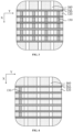
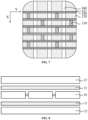
- FIGS. 1 to 7 are structural schematic diagrams of the solar cell provided by embodiments of the present disclosure.
- FIG. 1 is a structural schematic diagram of a solar cell provided by some embodiments of the present disclosure.
- FIG. 2 is a sectional schematic diagram along the dotted line AA in FIG. 1 of the solar cell provided by some embodiments of the present disclosure.
- FIG. 3 is a top view of a first solar cell provided by some embodiments of the present disclosure.
- FIG. 4 is a top view of a second solar cell provided by some embodiments of the present disclosure.
- FIG. 5 is a top view of a third solar cell provided by some embodiments of the present disclosure.
- FIG. 6 is a top view of a fourth solar cell provided by some embodiments of the present disclosure.
- FIG. 7 is a top view of a fifth solar cell provided by some embodiments of the present disclosure.
- the solar cell includes a substrate 100, a tunneling dielectric layer 110, a doped conductive layer 120, at least one conductive connection structure 130, a passivation layer 140 and a plurality of finger electrodes 150.
- the tunneling dielectric layer 110 is formed on the substrate 100.
- the doped conductive layer 120 is formed on the tunneling dielectric layer 110 and has a plurality of protrusions 121 arranged along a first direction X, each protrusion 121 of the plurality of protrusions 121 extends along a second direction Y perpendicular to the first direction X.
- the at least one conductive connection structure 130 is formed between two adjacent protrusions 121 and is connected with sidewalls of the two adjacent protrusions 121.
- the passivation layer 140 is over the doped conductive layer 120 and the at least one conductive connection structure 130.
- Each finger electrode 150 of the plurality of finger electrodes 150 extends along the second direction Y to penetrate the passivation layer 140 and connect to a respective protrusion 121.
- the substrate 100 is a silicon substrate, which may include one or more of monocrystalline silicon, polycrystalline silicon, amorphous silicon or microcrystalline silicon.
- the material of the substrate 100 may include silicon carbide, organic material or multicomponent compound.
- the multicomponent compound may include, but is not limited to, perovskite, gallium arsenide, cadmium telluride, copper indium selenium and the like.
- the substrate 100 has N-type or P-type doping elements.
- N-type elements may be Group-V elements such as phosphorus (P), bismuth (Bi), antimony (Sb) or arsenic (As), and P-type elements may be Group-III elements such as boron (B), aluminum (Al), gallium (Ga) or indium (In).
- P-type elements may be Group-V elements such as phosphorus (P), bismuth (Bi), antimony (Sb) or arsenic (As)
- P-type elements may be Group-III elements such as boron (B), aluminum (Al), gallium (Ga) or indium (In).
- the substrate 100 is a P-type substrate
- the doping elements in the substrate are P-type elements.
- the substrate 100 is an N-type substrate
- the doping elements in the substrate are N-type elements.
- the tunneling dielectric layer 110 and the doped conductive layer 120 may form a passivation contact structure on the substrate 100.
- the formation of the tunneling dielectric layer 110 and the doped conductive layer 120 can reduce the recombination of carriers at surface of the solar cell and increase the open-circuit voltage of the solar cell, thereby improving the efficiency of the solar cell.
- the tunneling dielectric layer 110 may be formed on a first surface of the substrate 100. The first surface is a light receiving surface facing sunlight.
- the tunneling dielectric layer 110 may be formed on a second surface of the substrate 100. The second surface is a surface opposite to the first surface and facing away sunlight.
- the tunneling dielectric layer 110 may be formed on both the first surface and the second surface of the substrate 100 (not shown in FIG. 1 ). It should be understood that other layers on the tunneling dielectric layer 110 are also formed on the first surface and/or the second surface of the substrate 100 at the same time.
- the tunneling dielectric layer 110 may be further configured to reduce or prevent the diffusion of doping elements in the doped conductive layer 120 into the substrate 100.
- the materials of the tunneling dielectric layer 110 may include, but are not limited to, dielectric materials having tunneling effect such as aluminum oxide, silicon oxide, silicon nitride, silicon oxynitride, intrinsic amorphous silicon, intrinsic polycrystalline silicon and the like.
- the tunneling dielectric layer 110 may be formed by a layer of oxide of silicon (SiOx), which has good passivation characteristics, and carriers can easily tunnel through the layer of oxide of silicon.
- a thickness of the tunneling dielectric layer 110 may range from 0.5 nm to 2.5 nm. In some other embodiments, the thickness of the tunneling dielectric layer 110 ranges from 0.5 nm to 2 nm. In some other embodiments, the thickness of the tunneling dielectric layer 110 ranges from 0.5 nm to 1.2 nm. When the thickness of the tunneling dielectric layer 110 is less than 0.5 mm, it is difficult to form the tunneling dielectric layer 110. When the thickness of the tunneling dielectric layer 110 is greater than 2.5 mm, the tunneling effect is weak.
- the at least one conductive connection structure 130 and the doped conductive layer 120 are made of a same material.
- the materials of the conductive connection structure 130 include at least one of polycrystalline silicon, amorphous silicon or microcrystalline silicon.
- the protrusions 121 of the doped conductive layer 120 and the at least one conductive connection structure 130 may be formed at the same time.
- the protrusions 121 and the at least one conductive connection structure 130 are formed by etching the doped conductive layer 120 in a same process operation. In this way, the connection reliability between the protrusions 121 and the at least one conductive connection structure 130 can be secured, and the number of production operations in the generating process and production time can be reduced.
- the protrusions and the at least one conductive connection structure may be formed separately.
- the material of the doped conductive layer 120 may be one of doped amorphous silicon, doped polycrystalline silicon or doped microcrystalline silicon. In some other embodiments, the doped conductive layer 120 may be made of other materials, such as silicon carbide, which may be selected according to actual situation.
- a conductive layer may be first formed on the tunneling dielectric layer 110, and then dope the conductive layer to form the doped conductive layer 120.
- the thickness of the doped conductive layer 120 ranges from 40 nm to 150 nm. In some other embodiments, the thickness of the doped conductive layer 120 ranges from 60 nm to 90 nm. The above-mentioned ranges of thickness of the doped conductive layer 120 can ensure that the optical loss of the doped conductive layer 120 is low and the interface passivation effect of the tunneling dielectric layer 110 is good, thereby improving the efficiency of the solar cell.
- the material of the doped conductive layer may be polycrystalline silicon.
- the doped conductive layer 120 and the substrate 100 are of a same doping type. It can be understood that when the doping type of the substrate 100 is N type and the doping type of the doped conductive layer 120 is P type, the majority carriers in the substrate 100 are electrons and the majority carriers in the doped conductive layer 120 are holes, recombination will occur between the electrons and the holes, resulting in reduction of the carriers collected by the finger electrodes 150. Therefore, when the doped conductive layer 120 and the substrate 100 are of a same doping type, reduction of the carriers collected by the finger electrodes 150 can be prevented.
- the substrate 100 is an N-type substrate, and the doped conductive layer 120 is an N-type polycrystalline silicon layer.
- the substrate is a P-type substrate, and the doped conductive layer is a P-type polycrystalline silicon layer.
- the N-type substrate and N-type polycrystalline silicon layer have relatively high photoelectric conversion efficiency.
- the formation process of the P-type substrate and P-type polycrystalline silicon layer is simple and can be selected according to the actual situation.
- the embodiments of the present disclosure do not limit the substrate 100 and the doped conductive layer 120.
- the conductive connection structure 130 and the protrusions 121 are formed by etching the doped conductive layer 120.
- the shape of the doped conductive layer 120 may be set first, and then the doped conductive layer 120 is etched to form the protrusions 121 and the conductive connection structure 130 in a same process operation.
- the passivation layer 140 may be an antireflection film layer. In this way, the light reflected by the surface of the solar cell can be reduced, thereby increasing the light transmittance of the solar cell.
- the passivation layer 140 may have a single-layer structure or a stacked-layers structure, and the materials of the passivation layer 140 may include one or more of silicon oxide, silicon nitride, silicon oxynitride, silicon oxycarbonitride, titanium oxide, hafnium oxide, aluminum oxide or the like.
- the passivation layer 140 is a hydrogen containing passivation layer, for example, the passivation layer is made of silicon oxide containing hydrogen, silicon nitride containing hydrogen, silicon oxynitride containing hydrogen and the like.
- the plurality of finger electrodes 150 is used to collect and converge the currents of the solar cell.
- the finger electrodes 150 may be obtained by sintering firing-through paste.
- the materials of the finger electrodes 150 may include one or more of aluminum, silver, gold, nickel, molybdenum or copper.
- the finger electrodes 150 refer to thin grid lines or finger grid lines, which are different from the main grid lines or busbars.
- the solar cell includes a plurality of conductive connection structures 130 arranged at intervals along at least one of the first direction X and the second direction Y, and there is at least one finger electrode 150 between adjacent conductive connection structures 130 in the first direction X.
- the plurality of conductive connection structures 130 may be arranged at intervals along the first direction X, the second direction Y or the first direction X and the second direction Y.
- the first direction X there is at least one finger electrode 150 between adjacent conductive connection structures 130.
- there is one finger electrode 150 between adjacent conductive connection structures 130 there is one or more conductive connection structures 130 between every two adjacent protrusions.
- the conductive connection structures 130 may be distributed in a spaced manner. For example, in the first direction, there is one or more conductive connection structures 130 between a first and a second finger electrodes, but there is no conductive connection structure 130 between the second and a third finger electrodes.
- the transverse transferring capacity of the solar cell can be improved.
- first finger electrode, second finger electrode and third finger electrode are only used to illustrate, and do not constitute a limit to the finger electrodes 150.
- the conductive connection structures 130 may be arranged in a regular manner. For example, there is one or more conductive connection structures 130 between a first and a second finger electrodes, there is no conductive connection structure 130 between the second and a third finger electrodes, and there is one or more conductive connection structures 130 between the third and a fourth finger electrodes, and so on.
- connection structures 130 there is one or more conductive connection structures 130 between the first and the second finger electrodes, there is one or more conductive connection structures 130 between the second and the third finger electrodes, there is no conductive connection structure 130 between the third and the fourth finger electrodes, and there is one or more conductive connection structures 130 between the fourth and a fifth finger electrodes, and so on.
- the conductive connection structures 130 may be arranged in an irregular manner.
- a distance between adjacent conductive connection structures 130 of the plurality of conductive connection structures 130 arranged at intervals is constant. In this way, it is convenient to the laser ablation process in the generating process, in other word, there is no need of adjusting the distance between adjacent conductive connection structures, thereby being convenient to the production.
- a distance between adjacent conductive connection structures 130 in the second direction ranges from 0.01 mm to 20 mm, such as 0.1 mm, 0.5 mm, 10 mm or the like.
- the distance between adjacent conductive connection structures 130 is less than 0.01 mm, excessively serried conductive connection structures 130 may cause serious light absorption, which is not conducive to improving the photoelectric conversion efficiency of the solar cell.
- the distance between adjacent conductive connection structures 130 is greater than 20 mm, excessively few conductive connection structures 130 cannot provide improving effect good enough.
- the distance between adjacent conductive connection structures 130 may have other values, which may be determined according to actual situation, embodiments of the present disclosure do not limit the distance between adjacent conductive connection structures 130.
- the plurality of conductive connection structures 130 form an array, and the array includes a plurality of columns of conductive connection structures 130 arranged along the first direction X and a plurality of rows of conductive connection structures 130 arranged along the second direction Y.
- the plurality of conductive connection structures 130 are arranged in a regular manner along the first direction X and the second direction Y. In this way, the transverse transferring capacity of the solar cell can be improved, and the production difficulty of forming the plurality of conductive connection structures 130 can be reduced.
- any conductive connection structure of the first column of conductive connection structures and a respective conductive connection structure of the second column of conductive connection structures are in a same row.
- any conductive connection structure of the first column of conductive connection structures and a respective conductive connection structure of the second column of conductive connection structures may be not in a same row.
- the first and second column of conductive connection structures are arranged in a stagger manner relative to each other.
- some conductive connection structures of the first column of conductive connection structures and respective conductive connection structures of the second column of conductive connection structures are respectively arranged in a same row.
- the present disclosure does not specifically limit the conductive connection structures 130, as long as the plurality of conductive connection structures 130 form an array.
- a width of the at least one conductive connection structure 130 in the second direction Y ranges from 10 ⁇ m to 500 ⁇ m, such as 50 ⁇ m, 80 ⁇ m, 100 ⁇ m or the like. It should be understood that when the width of the at least one conductive connection structure 130 is less than 10 ⁇ m, the transverse transferring capacity of each conductive connection structure 130 is weak, and the conductive connection structure cannot provide good improving effect. When the width of the at least one conductive connection structure 130 is greater than 500 ⁇ m, the conductive connection structure 130 may have a high-level parasitic absorption of light, which is detrimental to the improvement of photoelectric conversion efficiency of the solar cell. In some other embodiments, the width of the at least one conductive connection structure 130 may have other values, which may be determined according to actual situation.
- a top surface of the at least one conductive connection structure 130 is lower than or flush with a top surface of a protrusion 121.
- a thickness of the at least one conductive connection structure 130 is less than or equal to a thickness of a protrusion 121.
- the production process of the solar cell can be simplified, and the protrusions 121 and the at least one conductive connection structure 130 can be formed in a same process operation by laser ablation.
- the top surface of the conductive connection structure 130 may be higher than the top surface of the protrusion 121, which may be determined according to actual situation.
- a height of the at least one conductive connection structure 130 may be 0.5 to 1.2 times of a height of a protrusion 121.
- the conductive connection structure 130 is relatively thin, which results in a relatively weak transverse transferring capacity and a not prominent improvement.
- the conductive connection structure 130 is relatively thick, which results in a relatively strong capacity of parasitic absorption of light of the conductive connection structure 130 and therefore a reduction in the photoelectric conversion efficiency of the solar cell.
- the solar cell further includes at least one busbar 160 extending along the first direction X and electrically connected with the plurality of finger electrodes 150 arranged along the first direction X. Through the at least one busbar 160, the currents collected by the plurality of finger electrodes 150 can be converged and outputted from the solar cell.
- the plurality of conductive connection structures 130 are spaced from the at least one busbar 160. In this way, the at least one busbar 160 can be limited by the plurality of conductive connection structures 130, which is conducive to the subsequent printing of the at least one busbar 160. Moreover, the position of the at least one busbar 160 can be determined without additional positioning operation, which is conducive to the production operations.
- a column of conductive connection structures 130 arranged at intervals along the first direction X may be formed between adjacent busbars 160. In some other embodiments, more than one column of conductive connection structures 130 arranged at intervals along the first direction X may be formed between adjacent busbars 160. The present disclosure does not limit the number of the conductive connection structures 130 between adjacent busbars 160, which may be determined according to actual situation.
- projections of the plurality of conductive connection structures 130 on the substrate 100 are at least partially overlapped with a projection of the at least one busbar 160 on the substrate 100.
- the busbar 160 is generally of non-sintered type and used to collect the photo-generated carriers collected by the plurality of finger electrodes 150. That is to say, the busbar 160 will not corrode the structure under the busbar 160, so that the conductive connection structures 130 formed under the busbar 160 will not be affected by the busbar. Therefore, the transverse transferring capacity of the conductive connection structures 130 will not be affected.
- the busbar 160 that at least shields a part of each conductive connection structures 130 can reduce capacity of parasitic absorption of light of the conductive connection structures 130, thereby improving the photoelectric conversion efficiency of the solar cell.
- the solar cell includes a plurality of busbars, and there are at least two columns of conductive connection structures 130 arranged along the first direction X on a side of a peripheral busbar 160 towards an edge of the substrate. In some other embodiments, no conductive connection structure or one column of conductive connection structures arranged along the first direction is formed on the side of the peripheral busbar towards the edge of the substrate. By forming at least two columns of conductive connection structures 130, the number of the conductive connection structures 130 can be increased, thereby improving the transverse transferring capacity of the solar cell.
- the solar cell has a front surface and a rear surface.
- the front surface is a light receiving surface that absorbs incident light
- the rear surface is a surface opposite to the front surface.
- the tunneling dielectric layer 110, the doped conductive layer 120, the at least one conductive connection structure 130, the passivation layer 140 and the plurality of finger electrodes 150 may be respectively formed over the front surface and the rear surface of the solar cell.
- a doped conductive layer 120 formed over the rear surface of the solar cell and the substrate 100 are of a same doping type, and a doped conductive layer 120 formed over the front surface of the solar cell and the substrate 100 are of different doping types.
- doping type of the doped conductive layer 120 formed over the rear surface of the solar cell is N type
- doping type of the doped conductive layer 120 formed over the front surface of the solar cell is P type.
- the tunneling dielectric layer 110 and the doped conductive layer 120 are formed over the substrate 100, and the doped conductive layer 120 has a plurality of protrusions 121, thereby forming height differences on the doped conductive layer 120.
- the doped conductive layer 120 has a plurality of protrusions 121, thereby forming height differences on the doped conductive layer 120.
- contacts between the plurality of finger electrodes 150 and the doped conductive layer 120 can be ensured, and the parasitic absorption of light of the doped conductive layer 120 can be reduced.
- At least one conductive connection structure 130 is formed between adjacent protrusions 121 of the doped conductive layer 120, and the adjacent protrusions 121 are connected by the conductive connection structure 130. In this way, the transverse transferring capacity of the doped conductive layer 120 can be improved, thereby increasing the transfer rate of the solar cell.
- the photovoltaic module configured to convert the received light energy into electrical energy and transfer it to external loads.
- the photovoltaic module includes at least one cell string 10, at least one encapsulation layer 21 and at least one cover plate 22.
- the at least one cell string 10 includes a plurality of solar cells as described above (such as, FIGS. 1 to 4 ), and the plurality of solar cells are electrically connected in sequence.
- the at least one encapsulation layer is configured to cover a surface of the at least one cell string.
- the at least one cover plate is configured to cover a surface of the at least one encapsulation layer 21 facing away from the at least one cell string.
- the at least one encapsulation layer 21 may be an organic encapsulation adhesive film such as an ethylene vinyl acetate copolymer (EVA) adhesive film, or a polyethylene octene copolymer (POE) adhesive film.
- EVA ethylene vinyl acetate copolymer
- POE polyethylene octene copolymer
- the encapsulation layer 21 covers a surface of the cell string to seal and protect the cell string.
- the encapsulation layers 21 includes an upper encapsulation adhesive film and a lower encapsulation adhesive film that respectively cover an upper surface and a lower surface of the cell string.
- the at least one cover plate 22 may be a cover plate for protecting the cell string, such as a glass cover plate, a plastic cover plate or the like.
- the at least one cover plate 22 covers a surface of the encapsulation layer 21 facing away from the cell string.
- the cover plate 22 has a light trapping structure to increase the utilization rate of the incident light. In this way, the photovoltaic module can have high current-collection capacity, low carrier recombination rate, and therefore high photoelectric conversion efficiency.
- the cover plates 22 include an upper cover plate and a lower cover plate located on either sides of the cell string.
Landscapes
- Photovoltaic Devices (AREA)
- Life Sciences & Earth Sciences (AREA)
- Chemical & Material Sciences (AREA)
- Crystallography & Structural Chemistry (AREA)
- Sustainable Development (AREA)
Priority Applications (2)
| Application Number | Priority Date | Filing Date | Title |
|---|---|---|---|
| EP25179741.1A EP4586769A3 (de) | 2022-06-27 | 2023-02-03 | Solarzelle und fotovoltaisches modul |
| EP25187311.3A EP4604695A3 (de) | 2022-06-27 | 2023-02-03 | Solarzelle und fotovoltaisches modul |
Applications Claiming Priority (1)
| Application Number | Priority Date | Filing Date | Title |
|---|---|---|---|
| CN202210745275.2A CN116722055A (zh) | 2022-06-27 | 2022-06-27 | 一种太阳能电池及光伏组件 |
Related Child Applications (3)
| Application Number | Title | Priority Date | Filing Date |
|---|---|---|---|
| EP25187311.3A Division EP4604695A3 (de) | 2022-06-27 | 2023-02-03 | Solarzelle und fotovoltaisches modul |
| EP25179741.1A Division-Into EP4586769A3 (de) | 2022-06-27 | 2023-02-03 | Solarzelle und fotovoltaisches modul |
| EP25179741.1A Division EP4586769A3 (de) | 2022-06-27 | 2023-02-03 | Solarzelle und fotovoltaisches modul |
Publications (3)
| Publication Number | Publication Date |
|---|---|
| EP4300599A1 true EP4300599A1 (de) | 2024-01-03 |
| EP4300599C0 EP4300599C0 (de) | 2025-07-23 |
| EP4300599B1 EP4300599B1 (de) | 2025-07-23 |
Family
ID=85174173
Family Applications (3)
| Application Number | Title | Priority Date | Filing Date |
|---|---|---|---|
| EP23154994.0A Active EP4300599B1 (de) | 2022-06-27 | 2023-02-03 | Solarzelle und fotovoltaisches modul |
| EP25187311.3A Pending EP4604695A3 (de) | 2022-06-27 | 2023-02-03 | Solarzelle und fotovoltaisches modul |
| EP25179741.1A Pending EP4586769A3 (de) | 2022-06-27 | 2023-02-03 | Solarzelle und fotovoltaisches modul |
Family Applications After (2)
| Application Number | Title | Priority Date | Filing Date |
|---|---|---|---|
| EP25187311.3A Pending EP4604695A3 (de) | 2022-06-27 | 2023-02-03 | Solarzelle und fotovoltaisches modul |
| EP25179741.1A Pending EP4586769A3 (de) | 2022-06-27 | 2023-02-03 | Solarzelle und fotovoltaisches modul |
Country Status (7)
| Country | Link |
|---|---|
| US (2) | US12376421B2 (de) |
| EP (3) | EP4300599B1 (de) |
| JP (1) | JP2024003746A (de) |
| CN (1) | CN116722055A (de) |
| AU (1) | AU2023200098B2 (de) |
| DE (1) | DE202023101198U1 (de) |
| NL (1) | NL2034431B1 (de) |
Families Citing this family (6)
| Publication number | Priority date | Publication date | Assignee | Title |
|---|---|---|---|---|
| AU2022241631B1 (en) | 2022-08-05 | 2024-01-04 | Jinko Solar Co., Ltd. | Solar cell and photovoltaic module |
| CN116895703A (zh) | 2022-08-05 | 2023-10-17 | 浙江晶科能源有限公司 | 太阳能电池及光伏组件 |
| CN118039708B (zh) * | 2024-03-08 | 2025-06-27 | 天合光能股份有限公司 | 太阳能电池及其制作方法、光伏组件及光伏系统 |
| CN117936606B (zh) * | 2024-03-21 | 2024-08-09 | 晶科能源(海宁)有限公司 | 太阳能电池及光伏组件 |
| CN118676224A (zh) * | 2024-06-11 | 2024-09-20 | 浙江晶科能源有限公司 | 太阳能电池及叠层电池 |
| CN119815983B (zh) * | 2024-12-10 | 2026-02-10 | 隆基绿能科技股份有限公司 | 太阳能电池片及光伏组件 |
Citations (6)
| Publication number | Priority date | Publication date | Assignee | Title |
|---|---|---|---|---|
| KR20160097926A (ko) * | 2015-02-10 | 2016-08-18 | 엘지전자 주식회사 | 태양 전지 |
| CN108666393A (zh) * | 2018-07-16 | 2018-10-16 | 英利能源(中国)有限公司 | 太阳能电池的制备方法及太阳能电池 |
| CN110690297A (zh) * | 2019-10-12 | 2020-01-14 | 通威太阳能(安徽)有限公司 | 一种p型隧穿氧化物钝化接触太阳能电池及其制备方法 |
| CN210897294U (zh) * | 2019-10-29 | 2020-06-30 | 苏州阿特斯阳光电力科技有限公司 | 太阳能电池 |
| CN112349798A (zh) * | 2020-10-27 | 2021-02-09 | 浙江晶科能源有限公司 | 太阳能电池及其制造方法 |
| EP4002493A1 (de) * | 2020-11-19 | 2022-05-25 | Jinko Green Energy (Shanghai) Management Co., Ltd | Solarzelle |
Family Cites Families (27)
| Publication number | Priority date | Publication date | Assignee | Title |
|---|---|---|---|---|
| US6114046A (en) * | 1997-07-24 | 2000-09-05 | Evergreen Solar, Inc. | Encapsulant material for solar cell module and laminated glass applications |
| JPH11274538A (ja) | 1998-01-20 | 1999-10-08 | Sharp Corp | 高強度薄型半導体素子形成用基板、高強度薄型半導体素子及び高強度薄型半導体素子の製造方法 |
| US7659627B2 (en) * | 2007-12-05 | 2010-02-09 | Fujifilm Corporation | Photodiode |
| JP5449849B2 (ja) | 2009-04-30 | 2014-03-19 | シャープ株式会社 | 太陽電池およびその製造方法 |
| WO2011065571A1 (ja) | 2009-11-30 | 2011-06-03 | 京セラ株式会社 | 光電変換モジュールおよびその製造方法ならびに発電装置 |
| KR20120012555A (ko) * | 2010-08-02 | 2012-02-10 | 광주과학기술원 | 점진적으로 굴절률이 변하는 실리콘 다층 무반사막 및 그 제조방법 및 이를 구비하는 태양전지 및 그 제조방법 |
| CN102593204B (zh) * | 2011-01-10 | 2014-09-24 | Lg电子株式会社 | 太阳能电池和制造该太阳能电池的方法 |
| KR101729311B1 (ko) | 2011-02-22 | 2017-04-21 | 엘지전자 주식회사 | 태양 전지 및 그 제조 방법 |
| GB2509097A (en) * | 2012-12-19 | 2014-06-25 | Rec Cells Pte Ltd | Photovoltaic cell element having a specific electrode configuration |
| US9722104B2 (en) | 2014-11-28 | 2017-08-01 | Lg Electronics Inc. | Solar cell and method for manufacturing the same |
| JP6238884B2 (ja) | 2014-12-19 | 2017-11-29 | 三菱電機株式会社 | 光起電力素子およびその製造方法 |
| KR101740523B1 (ko) | 2015-12-21 | 2017-05-26 | 엘지전자 주식회사 | 태양 전지 및 그 제조 방법 |
| NL2017872B1 (en) | 2016-11-25 | 2018-06-08 | Stichting Energieonderzoek Centrum Nederland | Photovoltaic cell with passivating contact |
| EP3358627B1 (de) * | 2017-02-07 | 2024-11-13 | Shangrao Xinyuan YueDong Technology Development Co. Ltd | Solarzelle |
| JP2019179838A (ja) | 2018-03-30 | 2019-10-17 | パナソニック株式会社 | 太陽電池セル、及び、太陽電池セルの製造方法 |
| CN210272384U (zh) | 2019-10-29 | 2020-04-07 | 协鑫集成科技股份有限公司 | 一种后刻蚀式n型接触钝化电池 |
| CN112259621A (zh) | 2020-11-11 | 2021-01-22 | 通威太阳能(安徽)有限公司 | 一种高效perc太阳能电池及其制备方法 |
| CN112466961B (zh) | 2020-11-19 | 2024-05-10 | 晶科绿能(上海)管理有限公司 | 太阳能电池及其制造方法 |
| CN214336723U (zh) | 2020-12-04 | 2021-10-01 | 一道新能源科技(衢州)有限公司 | 一种太阳能电池 |
| CN112635592B (zh) | 2020-12-23 | 2025-01-10 | 泰州隆基乐叶光伏科技有限公司 | 一种太阳能电池及其制作方法 |
| CN214477490U (zh) | 2020-12-29 | 2021-10-22 | 通威太阳能(金堂)有限公司 | 太阳能电池片 |
| CN113299770A (zh) | 2021-06-04 | 2021-08-24 | 浙江爱旭太阳能科技有限公司 | 一种选择性接触区域掩埋型太阳能电池及其背面接触结构 |
| CN113471321A (zh) | 2021-07-23 | 2021-10-01 | 常州时创能源股份有限公司 | 一种TOPCon太阳能电池及制造方法 |
| CN113571604B (zh) | 2021-09-27 | 2022-01-25 | 浙江晶科能源有限公司 | 光伏电池及其制备方法、光伏组件 |
| JP7168800B1 (ja) | 2021-12-09 | 2022-11-09 | ジョジアン ジンコ ソーラー カンパニー リミテッド | 太陽電池及び光起電力モジュール |
| CN115101619B (zh) | 2022-06-07 | 2025-03-14 | 中国科学院宁波材料技术与工程研究所 | 一种基于隧穿氧化层钝化接触结构的选择性发射极及其制备方法和应用 |
| CN116722060A (zh) | 2022-09-28 | 2023-09-08 | 浙江晶科能源有限公司 | 太阳能电池及光伏组件 |
-
2022
- 2022-06-27 CN CN202210745275.2A patent/CN116722055A/zh active Pending
-
2023
- 2023-01-09 AU AU2023200098A patent/AU2023200098B2/en active Active
- 2023-02-02 US US18/163,871 patent/US12376421B2/en active Active
- 2023-02-03 EP EP23154994.0A patent/EP4300599B1/de active Active
- 2023-02-03 EP EP25187311.3A patent/EP4604695A3/de active Pending
- 2023-02-03 EP EP25179741.1A patent/EP4586769A3/de active Pending
- 2023-02-10 JP JP2023018906A patent/JP2024003746A/ja active Pending
- 2023-03-13 DE DE202023101198.5U patent/DE202023101198U1/de active Active
- 2023-03-26 NL NL2034431A patent/NL2034431B1/en active
-
2025
- 2025-06-23 US US19/246,422 patent/US20250318321A1/en active Pending
Patent Citations (6)
| Publication number | Priority date | Publication date | Assignee | Title |
|---|---|---|---|---|
| KR20160097926A (ko) * | 2015-02-10 | 2016-08-18 | 엘지전자 주식회사 | 태양 전지 |
| CN108666393A (zh) * | 2018-07-16 | 2018-10-16 | 英利能源(中国)有限公司 | 太阳能电池的制备方法及太阳能电池 |
| CN110690297A (zh) * | 2019-10-12 | 2020-01-14 | 通威太阳能(安徽)有限公司 | 一种p型隧穿氧化物钝化接触太阳能电池及其制备方法 |
| CN210897294U (zh) * | 2019-10-29 | 2020-06-30 | 苏州阿特斯阳光电力科技有限公司 | 太阳能电池 |
| CN112349798A (zh) * | 2020-10-27 | 2021-02-09 | 浙江晶科能源有限公司 | 太阳能电池及其制造方法 |
| EP4002493A1 (de) * | 2020-11-19 | 2022-05-25 | Jinko Green Energy (Shanghai) Management Co., Ltd | Solarzelle |
Also Published As
| Publication number | Publication date |
|---|---|
| NL2034431A (en) | 2024-01-08 |
| AU2023200098A1 (en) | 2024-01-18 |
| EP4604695A3 (de) | 2025-10-15 |
| DE202023101198U1 (de) | 2023-05-17 |
| EP4300599C0 (de) | 2025-07-23 |
| EP4300599B1 (de) | 2025-07-23 |
| EP4586769A2 (de) | 2025-07-16 |
| US20250318321A1 (en) | 2025-10-09 |
| EP4586769A3 (de) | 2025-10-15 |
| NL2034431B1 (en) | 2025-02-04 |
| US20230420580A1 (en) | 2023-12-28 |
| EP4604695A2 (de) | 2025-08-20 |
| JP2024003746A (ja) | 2024-01-15 |
| CN116722055A (zh) | 2023-09-08 |
| AU2023200098B2 (en) | 2024-04-04 |
| US12376421B2 (en) | 2025-07-29 |
Similar Documents
| Publication | Publication Date | Title |
|---|---|---|
| AU2023200098B2 (en) | Solar cell and photovoltaic module | |
| US12575219B2 (en) | Solar cell and photovoltaic module | |
| US11621359B1 (en) | Solar cell, photovoltaic module, and method for preparing the solar cell | |
| US12176448B2 (en) | Photovoltaic cell and photovoltaic module | |
| US12471389B2 (en) | Solar cell, method for preparing the same, and photovoltaic module | |
| US20260075985A1 (en) | Solar cell and method for preparing the same, tandem solar cell, and photovoltaic module | |
| JP7470762B2 (ja) | 太陽電池および光起電力モジュール | |
| US12527111B2 (en) | Solar cell and photovoltaic module | |
| US20250255032A1 (en) | Solar cell and photovoltaic module | |
| CN118073439A (zh) | 太阳能电池及光伏组件 | |
| US12543403B2 (en) | Solar cell, method for preparing solar cell, and photovoltaic module | |
| US20250331318A1 (en) | Photovoltaic module and method for manufacturing photovoltaic module | |
| CN115000198A (zh) | 太阳能电池及光伏组件 | |
| EP4579762A1 (de) | Solarzelle und fotovoltaisches modul | |
| CN118073440A (zh) | 光伏组件 |
Legal Events
| Date | Code | Title | Description |
|---|---|---|---|
| PUAI | Public reference made under article 153(3) epc to a published international application that has entered the european phase |
Free format text: ORIGINAL CODE: 0009012 |
|
| STAA | Information on the status of an ep patent application or granted ep patent |
Free format text: STATUS: REQUEST FOR EXAMINATION WAS MADE |
|
| 17P | Request for examination filed |
Effective date: 20230203 |
|
| AK | Designated contracting states |
Kind code of ref document: A1 Designated state(s): AL AT BE BG CH CY CZ DE DK EE ES FI FR GB GR HR HU IE IS IT LI LT LU LV MC ME MK MT NL NO PL PT RO RS SE SI SK SM TR |
|
| STAA | Information on the status of an ep patent application or granted ep patent |
Free format text: STATUS: EXAMINATION IS IN PROGRESS |
|
| 17Q | First examination report despatched |
Effective date: 20240425 |
|
| REG | Reference to a national code |
Ref country code: DE Ref legal event code: R079 Free format text: PREVIOUS MAIN CLASS: H01L0031074500 Ipc: H10F0010165000 Ref document number: 602023004917 Country of ref document: DE |
|
| GRAP | Despatch of communication of intention to grant a patent |
Free format text: ORIGINAL CODE: EPIDOSNIGR1 |
|
| STAA | Information on the status of an ep patent application or granted ep patent |
Free format text: STATUS: GRANT OF PATENT IS INTENDED |
|
| RIC1 | Information provided on ipc code assigned before grant |
Ipc: H10F 77/30 20250101ALI20250312BHEP Ipc: H10F 77/20 20250101ALI20250312BHEP Ipc: H10F 77/14 20250101ALI20250312BHEP Ipc: H10F 10/166 20250101ALI20250312BHEP Ipc: H10F 10/165 20250101AFI20250312BHEP |
|
| INTG | Intention to grant announced |
Effective date: 20250407 |
|
| GRAS | Grant fee paid |
Free format text: ORIGINAL CODE: EPIDOSNIGR3 |
|
| GRAA | (expected) grant |
Free format text: ORIGINAL CODE: 0009210 |
|
| STAA | Information on the status of an ep patent application or granted ep patent |
Free format text: STATUS: THE PATENT HAS BEEN GRANTED |
|
| AK | Designated contracting states |
Kind code of ref document: B1 Designated state(s): AL AT BE BG CH CY CZ DE DK EE ES FI FR GB GR HR HU IE IS IT LI LT LU LV MC ME MK MT NL NO PL PT RO RS SE SI SK SM TR |
|
| REG | Reference to a national code |
Ref country code: GB Ref legal event code: FG4D |
|
| REG | Reference to a national code |
Ref country code: CH Ref legal event code: EP |
|
| REG | Reference to a national code |
Ref country code: DE Ref legal event code: R096 Ref document number: 602023004917 Country of ref document: DE |
|
| REG | Reference to a national code |
Ref country code: IE Ref legal event code: FG4D |
|
| U01 | Request for unitary effect filed |
Effective date: 20250804 |
|
| U07 | Unitary effect registered |
Designated state(s): AT BE BG DE DK EE FI FR IT LT LU LV MT NL PT RO SE SI Effective date: 20250813 |
|
| PG25 | Lapsed in a contracting state [announced via postgrant information from national office to epo] |
Ref country code: IS Free format text: LAPSE BECAUSE OF FAILURE TO SUBMIT A TRANSLATION OF THE DESCRIPTION OR TO PAY THE FEE WITHIN THE PRESCRIBED TIME-LIMIT Effective date: 20251123 |
|
| PG25 | Lapsed in a contracting state [announced via postgrant information from national office to epo] |
Ref country code: NO Free format text: LAPSE BECAUSE OF FAILURE TO SUBMIT A TRANSLATION OF THE DESCRIPTION OR TO PAY THE FEE WITHIN THE PRESCRIBED TIME-LIMIT Effective date: 20251023 |
|
| PG25 | Lapsed in a contracting state [announced via postgrant information from national office to epo] |
Ref country code: HR Free format text: LAPSE BECAUSE OF FAILURE TO SUBMIT A TRANSLATION OF THE DESCRIPTION OR TO PAY THE FEE WITHIN THE PRESCRIBED TIME-LIMIT Effective date: 20250723 |
|
| PG25 | Lapsed in a contracting state [announced via postgrant information from national office to epo] |
Ref country code: GR Free format text: LAPSE BECAUSE OF FAILURE TO SUBMIT A TRANSLATION OF THE DESCRIPTION OR TO PAY THE FEE WITHIN THE PRESCRIBED TIME-LIMIT Effective date: 20251024 |
|
| PG25 | Lapsed in a contracting state [announced via postgrant information from national office to epo] |
Ref country code: PL Free format text: LAPSE BECAUSE OF FAILURE TO SUBMIT A TRANSLATION OF THE DESCRIPTION OR TO PAY THE FEE WITHIN THE PRESCRIBED TIME-LIMIT Effective date: 20250723 |
|
| PG25 | Lapsed in a contracting state [announced via postgrant information from national office to epo] |
Ref country code: RS Free format text: LAPSE BECAUSE OF FAILURE TO SUBMIT A TRANSLATION OF THE DESCRIPTION OR TO PAY THE FEE WITHIN THE PRESCRIBED TIME-LIMIT Effective date: 20251023 |
|
| PG25 | Lapsed in a contracting state [announced via postgrant information from national office to epo] |
Ref country code: ES Free format text: LAPSE BECAUSE OF FAILURE TO SUBMIT A TRANSLATION OF THE DESCRIPTION OR TO PAY THE FEE WITHIN THE PRESCRIBED TIME-LIMIT Effective date: 20250723 |
|
| U20 | Renewal fee for the european patent with unitary effect paid |
Year of fee payment: 4 Effective date: 20260225 |
|
| PG25 | Lapsed in a contracting state [announced via postgrant information from national office to epo] |
Ref country code: SM Free format text: LAPSE BECAUSE OF FAILURE TO SUBMIT A TRANSLATION OF THE DESCRIPTION OR TO PAY THE FEE WITHIN THE PRESCRIBED TIME-LIMIT Effective date: 20250723 |
|
| PG25 | Lapsed in a contracting state [announced via postgrant information from national office to epo] |
Ref country code: CZ Free format text: LAPSE BECAUSE OF FAILURE TO SUBMIT A TRANSLATION OF THE DESCRIPTION OR TO PAY THE FEE WITHIN THE PRESCRIBED TIME-LIMIT Effective date: 20250723 |
|
| PG25 | Lapsed in a contracting state [announced via postgrant information from national office to epo] |
Ref country code: SK Free format text: LAPSE BECAUSE OF FAILURE TO SUBMIT A TRANSLATION OF THE DESCRIPTION OR TO PAY THE FEE WITHIN THE PRESCRIBED TIME-LIMIT Effective date: 20250723 |