EP4307646A1 - Ensemble carte de circuit imprimé et dispositif électronique - Google Patents
Ensemble carte de circuit imprimé et dispositif électronique Download PDFInfo
- Publication number
- EP4307646A1 EP4307646A1 EP22766320.0A EP22766320A EP4307646A1 EP 4307646 A1 EP4307646 A1 EP 4307646A1 EP 22766320 A EP22766320 A EP 22766320A EP 4307646 A1 EP4307646 A1 EP 4307646A1
- Authority
- EP
- European Patent Office
- Prior art keywords
- bracket
- flexible printed
- printed circuit
- circuit board
- main control
- Prior art date
- Legal status (The legal status is an assumption and is not a legal conclusion. Google has not performed a legal analysis and makes no representation as to the accuracy of the status listed.)
- Granted
Links
Images



Classifications
-
- H—ELECTRICITY
- H04—ELECTRIC COMMUNICATION TECHNIQUE
- H04M—TELEPHONIC COMMUNICATION
- H04M1/00—Substation equipment, e.g. for use by subscribers
- H04M1/02—Constructional features of telephone sets
- H04M1/0202—Portable telephone sets, e.g. cordless phones, mobile phones or bar type handsets
- H04M1/026—Details of the structure or mounting of specific components
- H04M1/0277—Details of the structure or mounting of specific components for a printed circuit board assembly
-
- H—ELECTRICITY
- H05—ELECTRIC TECHNIQUES NOT OTHERWISE PROVIDED FOR
- H05K—PRINTED CIRCUITS; CASINGS OR CONSTRUCTIONAL DETAILS OF ELECTRIC APPARATUS; MANUFACTURE OF ASSEMBLAGES OF ELECTRICAL COMPONENTS
- H05K1/00—Printed circuits
- H05K1/02—Details
- H05K1/14—Structural association of two or more printed circuits
-
- H—ELECTRICITY
- H05—ELECTRIC TECHNIQUES NOT OTHERWISE PROVIDED FOR
- H05K—PRINTED CIRCUITS; CASINGS OR CONSTRUCTIONAL DETAILS OF ELECTRIC APPARATUS; MANUFACTURE OF ASSEMBLAGES OF ELECTRICAL COMPONENTS
- H05K1/00—Printed circuits
- H05K1/02—Details
- H05K1/14—Structural association of two or more printed circuits
- H05K1/148—Arrangements of two or more hingeably connected rigid printed circuit boards, i.e. connected by flexible means
-
- H—ELECTRICITY
- H04—ELECTRIC COMMUNICATION TECHNIQUE
- H04M—TELEPHONIC COMMUNICATION
- H04M1/00—Substation equipment, e.g. for use by subscribers
- H04M1/02—Constructional features of telephone sets
- H04M1/0202—Portable telephone sets, e.g. cordless phones, mobile phones or bar type handsets
- H04M1/026—Details of the structure or mounting of specific components
-
- H—ELECTRICITY
- H05—ELECTRIC TECHNIQUES NOT OTHERWISE PROVIDED FOR
- H05K—PRINTED CIRCUITS; CASINGS OR CONSTRUCTIONAL DETAILS OF ELECTRIC APPARATUS; MANUFACTURE OF ASSEMBLAGES OF ELECTRICAL COMPONENTS
- H05K1/00—Printed circuits
- H05K1/02—Details
- H05K1/14—Structural association of two or more printed circuits
- H05K1/147—Structural association of two or more printed circuits at least one of the printed circuits being bent or folded, e.g. by using a flexible printed circuit
-
- Y—GENERAL TAGGING OF NEW TECHNOLOGICAL DEVELOPMENTS; GENERAL TAGGING OF CROSS-SECTIONAL TECHNOLOGIES SPANNING OVER SEVERAL SECTIONS OF THE IPC; TECHNICAL SUBJECTS COVERED BY FORMER USPC CROSS-REFERENCE ART COLLECTIONS [XRACs] AND DIGESTS
- Y02—TECHNOLOGIES OR APPLICATIONS FOR MITIGATION OR ADAPTATION AGAINST CLIMATE CHANGE
- Y02E—REDUCTION OF GREENHOUSE GAS [GHG] EMISSIONS, RELATED TO ENERGY GENERATION, TRANSMISSION OR DISTRIBUTION
- Y02E60/00—Enabling technologies; Technologies with a potential or indirect contribution to GHG emissions mitigation
- Y02E60/10—Energy storage using batteries
Definitions
- This application relates to the field of terminal technologies, and in particular to a circuit board component and an electronic device.
- Embodiments of this application are intended to provide a circuit board component and an electronic device, which can resolve a problem that in the related art, an area utilization rate of a motherboard is low when by stacking the FPCs, wiring on an FPC is implemented.
- an embodiment of this application provides a circuit board component, including:
- an embodiment of this application further provides an electronic device, including the circuit board component according to the embodiment of the first aspect.
- a second bracket is disposed between a first flexible printed circuit and a first bracket, so that a problem that wiring on a second flexible printed circuit is implemented by stacking brackets can be resolved and it is unnecessary to dispose a fastener such as an additional screw to fasten the second bracket.
- a fastener such as an additional screw to fasten the second bracket.
- the fastener only needs to be used to connect the first bracket to the main control board by using the fastener, so that by stacking the FPCs, wiring on the second flexible printed circuit is implemented, and the second flexible printed circuit is pressed and fastened to the main control board or the BTB connector, thereby effectively saving the fasteners, improving a space utilization rate of the circuit board component, and further improving installation efficiency.
- circuit board component 110. main control board, 120. first flexible printed circuit; 121. first body; 122. reinforced member; 130. first bracket; 140. second bracket; 141. second body; 142. concave groove; 143. first support table; 144. second support table; 150. second flexible printed circuit; 160. fastener; 170. adhesive member; and 180. connector.
- a circuit board component provided in the embodiments of this application is mainly used for electronic devices, including but not limited to electronic devices such as mobile phones, tablet computers, laptop computers, mobile computers, and handheld game consoles.
- the electronic device may be used in devices other than the electronic devices.
- circuit board component 100 and an electronic device proposed in the embodiments of this application with reference to the accompanying drawings.
- FIG. 1 is a first schematic diagram of assembly of an FPC depicting a wiring method in the related art.
- FIG. 2 is an exploded diagram of assembly of an FPC depicting a wiring method in the related art.
- FIG. 3 is a second schematic diagram of assembly of an FPC depicting a wiring method in the related art.
- FIG. 4 is a third schematic diagram of assembly of an FPC depicting a wiring method in the related art.
- FIG. 5 is a partial view of assembly of an FPC depicting a wiring method in FIG. 4 enlarged at A.
- one FPC Flexible Printed Circuit
- a primary FPC 10' is directly buckled onto a primary FPC-BTB 30'.
- a motherboard bracket 20' directly presses a primary FPC-BTB reinforced steel plate 40' to prevent the primary FPC-BTB 30' from loosening.
- a secondary FPC 50' passes over the motherboard bracket 20'.
- the motherboard PCBA 60' must be installed first.
- the primary FPC 10' is assembled.
- the motherboard bracket 20' is assembled.
- the secondary FPC 50' is assembled.
- the BTB fastening bracket 70' is assembled. Therefore, for the secondary FPC 50', one separate BTB fastening bracket 70' must be designed and locked by using screws to ensure that the primary FPC-BTB 30' does not loosen.
- one separate BTB fastening bracket 70' is designed to press the primary FPC-BTB 30', both an assembly process and a disassembly method are complicated.
- usually two screws are needed to lock the BTB fastening bracket 70', or one screw and a patch clamping hook are used to fasten the BTB fastening bracket 70'. Therefore, there are problems, for example, excessive screws are used, and an area utilization rate of a motherboard is low.
- FIG. 6 is a first structural diagram of a circuit board component 100 according to an embodiment of this application.
- FIG. 7 is an exploded diagram of a circuit board component 100 according to an embodiment of this application.
- FIG. 8 is a second structural diagram of a circuit board component 100 according to an embodiment of this application.
- FIG. 9 is a third structural diagram of a circuit board component 100 according to an embodiment of this application.
- FIG. 10 is a partial view of the circuit board component 100 shown in the embodiment in FIG. 9 enlarged at B.
- the circuit board component 100 includes: a main control board 110; a first flexible printed circuit 120; a first bracket 130; a second bracket 140; a second flexible printed circuit 150; and a fastener 160. At least a part of the first flexible printed circuit 120 is disposed on the main control board 110.
- the first bracket 130 is located on a side of the first flexible printed circuit 120 away from the main control board 110, and the first bracket 130 is connected to the main control board 110.
- At least a part of the second bracket 140 is located between the first flexible printed circuit 120 and the first bracket 130, the second bracket 140 abuts against the first bracket 130, and the second bracket 140 is connected to the first flexible printed circuit 120.
- a part of the second flexible printed circuit 150 is located between the first bracket 130 and the second bracket 140.
- the first bracket 130 is connected to the main control board 110 by using the fastener 160.
- the circuit board component 100 includes a main control board 110, a first flexible printed circuit 120, a first bracket 130, a second bracket 140, a second flexible printed circuit 150, and a fastener 160.
- the first flexible printed circuit 120 is disposed on the main control board 110. It may be understood that the first flexible printed circuit 120 is electrically connected to the main control board 110. If a BTB connector is disposed on the main control board 110, the first flexible printed circuit 120 is electrically connected to the main control board 110 by using the BTB connector.
- the first bracket 130 is located on a side of the first flexible printed circuit 120 away from the main control board 110, and the second bracket 140 is disposed between the first flexible printed circuit 120 and the first bracket 130.
- a part of the second flexible printed circuit 150 is located between the first bracket 130 and the second bracket 140, so that when the fastener 160 fixedly connects the first bracket 130 to the main control board 110, a problem that by stacking the FPCs, wiring is implemented between the first flexible printed circuit 120 and the second flexible printed circuit 150 can be resolved.
- a BTB connector is installed on the main control board 110, the first flexible printed circuit 120 is directly pressed onto the BTB connector, and the first bracket 130 is connected to the main control board 110 by using the fastener 160. In this way, the BTB connector is pressed and fastened to the first flexible printed circuit 120 and the second flexible board, thereby providing space for a layout of the circuit board component 100.
- the second bracket 140 is disposed between the first flexible printed circuit 120 and the first bracket 130, so that a problem that by stacking the FPCs, wiring on the second flexible printed circuit 150 is implemented can be resolved and it is unnecessary to dispose the fastener 160 such as an additional screw to fasten the second bracket 140.
- the first bracket 130 only needs to be connected to the main control board 110 by using the fastener 160, so that wiring on the second flexible printed circuit 150 is implemented, and the second flexible printed circuit 150 is pressed and fastened to the main control board 110 or the BTB connector, thereby effectively saving the fasteners 160, improving a space utilization rate of the circuit board component 100, and further improving installation efficiency.
- the fastener 160 may include a screw.
- the first bracket 130 is connected to the main control board 110 by using the screw, thereby reducing assembly difficulty of the circuit board component 100 and improving assembly efficiency of the circuit board component 100.
- the circuit board component 100 further includes a plurality of connectors 180.
- the connector 180 is disposed on the main control board 110 and electrically connected to the main control board 110.
- the first flexible printed circuit 120 is first directly pressed onto one connector 180.
- at least a part of the second bracket 140 is disposed on the first flexible printed circuit 120, and the first bracket 130 is pressed onto the second bracket 140.
- the second flexible printed circuit 150 is disposed between the first bracket 130 and the second bracket 140.
- the first bracket 130 is connected to the main control board 110 by using the fastener 160 to press and fasten the connector 180 to the flexible printed circuit.
- it is unnecessary to design a separate connector fastening bracket to fasten the connector 180 thereby effectively simplifying an assembly process of the circuit board component 100 and saving screws. This further effectively improves a space utilization rate of the circuit board component 100.
- the second flexible printed circuit is provided in plurality, and a plurality of the second brackets are in a one-to-one correspondence with the plurality of second flexible printed circuits, so that by stacking the FPCs, wiring on the plurality of second flexible printed circuits is implemented, thereby implementing a multi-functional design of electronic devices such as mobile phones.
- the second bracket 140 includes a second body 141 and a wire passing port. At least a part of the second body abuts against the first bracket, and at least a part of the second body is connected to the first flexible printed circuit.
- the wire passing port is provided on the second body 141, and the second flexible printed circuit 150 passes through the wire passing port.
- the second bracket 140 includes a second body 141 and a wire passing port. Specifically, a wire passing port is provided on the second body 141.
- a wire passing port is provided on the second body 141.
- the second flexible printed circuit 150 When the second flexible printed circuit 150 is installed, a part of the second flexible printed circuit 150 can pass through the wire passing port to implement wiring.
- at least a part of the second bracket 140 abuts against the first bracket 130, and when the first bracket 130 is fixedly connected to the main control board 110, the second bracket 140, a part of the first flexible printed circuit 120, and a part of the second flexible printed circuit 150 are pressed and fastened to the main control board 110, so that wiring on the flexible printed circuit is implemented while the second flexible printed circuit 150 passes through the wire passing port of the second bracket 140.
- a quantity of the wire passing ports may be set according to an actual need.
- One second flexible printed circuit 150 passes through one wire passing port, and a plurality of the wire passing ports can implement wiring on a plurality of the second flexible printed circuits 150, thereby implementing wiring on a plurality of the flexible printed circuits and implementing a multi-functional design of electronic devices such as mobile phones.
- FIG. 11 is a first structural diagram of a second bracket 140 according to an embodiment of this application.
- FIG. 12 is a second structural diagram of a second bracket 140 according to an embodiment of this application.
- FIG. 13 is a third structural diagram of a second bracket 140 according to an embodiment of this application.
- the second body 141 is provided with a concave groove 142.
- An opening of the concave groove 142 faces towards the first bracket 130, and the concave groove 142 is configured as the wire passing port.
- the wire passing port includes a concave groove 142. Specifically, an opening of the concave groove 142 faces towards the first bracket 130. It may be understood that the wire passing port may include a through hole extending in a direction in which the second flexible printed circuit 150 passes in or out.
- the wire passing port is configured as the concave groove 142 and the opening of the concave groove 142 faces upwards, a part of the second flexible printed circuit 150 can be directly installed on the concave groove 142.
- an installation process of the circuit board component 100 can further be simplified, so that installation efficiency can be improved and the circuit board component 100 is easy to disassemble and repair.
- At least one second flexible printed circuit 150 is suspended in the air between the first bracket 130 and the second bracket 140.
- a part of the second flexible printed circuit 150 is suspended in the air between the first bracket 130 and the second bracket 140. That is, there is a given gap between a part of the second flexible printed circuit 150 and the first bracket 130, and there is also a given gap between a part of the second flexible printed circuit 150 and a groove wall of the concave groove 142 of the second bracket 140, so that after installation of the circuit board component 100 is completed, the part of the second flexible printed circuit 150 located between the first bracket 130 and the second bracket 140 still can move freely within a given degree.
- the gap between the second flexible printed circuit 150 and the first bracket 130 and the gap between the second flexible printed circuit 150 and the groove wall of the concave groove 142 may be set according to an actual need.
- the wire passing port is provided in plurality, and the plurality of wire passing ports are spaced apart on the second body 141.
- the wire passing port is provided in plurality, and the plurality of wire passing ports are spaced apart on the second body 141. Each wire passing port can implement wiring on the second flexible printed circuit 150. The plurality of wire passing ports are spaced apart on the second body 141, thereby implementing wiring on a plurality of flexible printed circuits.
- the wire passing port may be configured as the concave groove 142
- a plurality of concave grooves 142 are spaced apart on the second body 141.
- the second bracket 140 is in a shape of a long strip, and the plurality of concave grooves 142 may be spaced apart along a length direction of the second body 141. This can further reduce thickness of the circuit board component 100 in a Z-axis direction while wiring on a plurality of second flexible printed circuits 150 is implemented, thereby implementing ultra-thin design for electronic devices such as mobile phones.
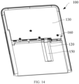
- FIG. 14 is a fourth structural diagram of a circuit board component 100 according to an embodiment of this application.
- FIG. 15 is an exploded diagram of a circuit board component 100 according to an embodiment of this application.
- FIG. 16 is a fifth structural diagram of a circuit board component 100 according to an embodiment of this application.
- FIG. 17 is a sixth structural diagram of a circuit board component 100 according to an embodiment of this application.
- FIG. 18 is a partial view of the circuit board component 100 shown in the embodiment in FIG. 17 enlarged at C.
- the second flexible printed circuit 150 is provided in plurality, and a plurality of the second brackets 140 are in a one-to-one correspondence with the plurality of second flexible printed circuits 150.
- the plurality of second brackets 140 are stacked on each other, and each second flexible printed circuit 150 passes through the corresponding wire passing port.
- the second flexible printed circuit 150 is provided in plurality, and the second bracket 140 is also provided in plurality.
- a quantity of the second flexible printed circuits 150 are in one-to-one corresponds to a quantity of the second brackets 140, and the plurality of second brackets 140 are stacked on each other. It may be understood that each second bracket 140 includes at least one wire passing port, thereby implementing, by stacking the FPCs, wiring on a plurality of flexible printed circuits.
- a plurality of the second brackets 140 may be stacked on each other along a height direction of the circuit board component 100. Except for the second bracket 140 that abuts against the first bracket 130 and the second bracket 140 that is connected to the first flexible printed circuit 120, a plurality of the second brackets 140 may abut against each other, so that by stacking the FPCs, wiring on a plurality of flexible printed circuits is implemented and when the first bracket 130 is fixedly connected to the main control board 110 by using the fastener 160, a plurality of the second brackets 140 can be pressed and fastened, thereby improving a fastening effect of the second bracket 140, effectively saving the fastener 160, and improving a space utilization rate of the circuit board component 100.
- the second bracket 140 further includes a first support table 143 and a second support table 144.
- the first support table 143 is disposed on a side of the second body 141 facing towards the first bracket 130.
- the second support table 144 is disposed on the side of the second body 141 facing towards the first bracket 130.
- the concave groove 142 is formed between the second support table 144 and the first support table 143.
- the first bracket 130 abuts against the first support table 143 and the second support table 144.
- the second bracket 140 further includes a first support table 143 and a second support table 144.
- the first support table 143 and the second support table 144 are disposed on a side of the second body 141 facing towards the first bracket 130.
- the first support table 143 and the second support table 144 forms the concave groove 142.
- a part of the second flexible printed circuit 150 passes through the concave groove 142 to implement wiring.
- the first bracket 130 abuts against the first support table 143 and the second support table 144, so that when the first bracket 130 is connected and fastened to the main control board 110 by using the fastener 160, the first bracket 130 and the second bracket 140 are pressed and fastened, the second bracket 140 and the first flexible printed circuit 120 are pressed and fastened, and the first flexible printed circuit 120 and the main control board 110 are pressed and fastened, thereby implementing wiring on the flexible printed circuit.
- this further avoids a problem in which in the related art, a motherboard bracket and a PCB need to be fastened while a separate connector fastening bracket needs to be designed to press a BTB connector, and at least two additional screws need to be disposed to fasten the BTB connector fastening bracket, thereby causing complicated disassembly and low installation efficiency. That is, this can effectively save screws, and improve a space utilization rate of the circuit board component 100 and installation efficiency of the circuit board component 100.
- a solution in which the first bracket 130 is in contact with the first support table 143 and the second support table 144 can reduce a contact area between the first bracket 130 and the second bracket 140. Therefore, when the first bracket 130 is connected to the main control board 110, the first bracket 130 and the second bracket 140 are pressed tighter, the second bracket 140 and the first flexible printed circuit 120 are pressed tighter, the first flexible printed circuit 120 and the main control board 110 are pressed tighter, further improving reliability of the circuit board component 100.
- an area in which the first support table 143 abuts against the first bracket 130 is equal to an area in which the second support table 144 abuts against the first bracket 130.
- an area in which the first support table 143 abuts against the first bracket 130 is equal to an area in which the second support table 144 abuts against the first bracket 130. That is, when the first bracket 130 is fixedly connected to the main control board 110 by using the fastener 160, the first support table 143 and the second support table 144 receive a same account of a pressing force, so that the first bracket 130 and the second bracket 140 is subject to a balanced force, and the second bracket 140 and the first flexible printed circuit 120 is subject to a balance force, thereby extending a service life of the circuit board component 100.
- the circuit board component 100 further includes a connector 180. If a position in which the second bracket 140 abuts against the first bracket 130 is subjected to an unbalanced force, a position in which the first flexible printed circuit 120 is in connect with the connector 180 is subject to an unbalanced force. Therefore, during a process in which the circuit board component 100 drops, the connector 180 is prone to problems, for example, a pad cracks.
- the foregoing solution effectively extends a service life of electronic devices such as mobile phones that are equipped with the circuit board component 100.
- first support table 143 and the second support table 144 are symmetrically disposed relative to the center of the second body 141.
- the first support table 143 and the second support table 144 are symmetrically disposed relative to the center of the second body 141. That is, when the first bracket 130 is fixedly connected to the main control board 110 by using the fastener 160, the first bracket 130 and the second bracket 140 may be subject to a balanced force, the second bracket 140 and the first flexible printed circuit 120 may be subject to a balanced force, thereby further extending a service life of the circuit board component 100.
- first support table 143 and the second support table 144 are respectively disposed at two ends of the second body 141. This ensures that various positions between the first bracket 130 and the second bracket 140 and between the second bracket 140 and the first flexible printed circuit 120 are subject to a balanced force while as much as space is provided for installation of the second flexible printed circuit 150, so as to ensure gaps between the second flexible printed circuit 150 and a groove wall of the concave groove 142 and between the second flexible printed circuit 150 and the first bracket 130, further extending a service life of the circuit board component 100.
- the first flexible printed circuit 120 includes a first body 121 and a reinforced member 122.
- the reinforced member 122 is disposed on a side of the first body 121 away from the main control board 110, and at least a part of the second bracket 140 is connected to the reinforced member 122.
- the first flexible printed circuit 120 includes a first body 121 and a reinforced member 122.
- a reinforced member 122 is disposed on a side of the first body 121 away from the main control board 110. That is, a reinforced member 122 is disposed on a side of the first body 121 near the second bracket 140, and the second bracket 140 is disposed on the reinforced member 122, so that structural strength of connection positions between the first flexible printed circuit 120 and the connector 180 and between the first flexible printed circuit 120 and the second bracket 140 can be improved, thereby avoiding a situation in which the connector 180 is prone to problems, for example, a pad cracks during a process in which the circuit board component 100 drops. This effectively extends a service life of electronic devices such as mobile phones that are equipped with the circuit board component 100.
- the reinforced member 122 needs to be a thick, rigid, and high-strength stainless steel material.
- a force transferred from the first support table 143 and the second support table 144 on two sides of the second bracket 140 can be evenly distributed on the reinforced member 122. If stiffness and strength of the reinforced member 122 are low, during a process in which the circuit board component 100 drop, the connector 180 is prone to problems, for example, a pad cracks.
- the circuit board component 100 further includes an adhesive member 170.
- the adhesive member 170 is disposed between the reinforced member 122 and the second bracket 140.
- the circuit board component 100 further includes an adhesive member 170.
- the adhesive member 170 is disposed between the reinforced member 122 and the second bracket 140. That is, the second bracket 140 is glued to the reinforced member 122 by using the adhesive member 170, so that the second bracket 140 is further fastened, thereby improving stability and reliability of the circuit board component 100, further simplifying an installation process of the circuit board component 100, reducing installation difficulty of the circuit board component 100, and improving installation efficiency of the circuit board component 100.
- the adhesive member 170 includes a double-sided adhesive tape.
- the main control board 110 is provided with a connector 180, and the first flexible printed circuit 120 is electrically connected to the main control board 110 by using the connector 180.
- the main control board 110 is provided with a connector 180, and the connector 180 is electrically connected to the main control board 110.
- the first flexible printed circuit 120 is electrically connected to the main control board 110 by using the connector 180, thereby implementing connection of each circuit on the circuit board component 100.
- the first flexible printed circuit 120 is directly pressed to the connector 180.
- the reinforced member 122 is disposed on a side of the first body 121 away from the connector 180.
- the second bracket 140 is connected to the reinforced member 122 by using the adhesive member 170.
- the first bracket 130 abuts against the first support table 143 and the second support table 144 of the second bracket 140.
- a part of the second flexible printed circuit 150 passes through the concave groove 142 of the second bracket 140.
- the first bracket 130 is fixedly connected to the main control board 110 by using the fastener 160. Therefore, connection between the first flexible printed circuit 120 and the connector 180 is completed, thereby providing space for a layout of the circuit board component 100.
- fastener 160 such as an additional screw to fasten the second bracket 140.
- wiring on the second flexible printed circuit 150 is implemented, and this avoids a problem in which in the related art, a motherboard bracket and a PCB need to be fastened while a separate connector fastening bracket needs to be designed to press a BTB connector, and at least two additional screws need to be disposed to fasten the BTB connector fastening bracket, thereby causing complicated disassembly and low installation efficiency.
- the first bracket 130 only needs to be connected to the main control board 110 by using the fastener 160, so that wiring on the second flexible printed circuit 150 is implemented, and the second flexible printed circuit 150 is pressed and fastened to the main control board 110 or the BTB connector, thereby effectively saving the fasteners 160, improving a space utilization rate of the circuit board component 100, and further improving installation efficiency.
- the electronic device proposed in this embodiment has the circuit board component 100 according to any one of the foregoing embodiments
- the electronic device has all the beneficial effects of the circuit board component 100 according to any one of the foregoing embodiments. Details are not described herein again.
- the electronic device further includes a housing.
- the first bracket 130 is provided with a first connecting hole
- the main control board 110 is provided with a second connecting hole
- the housing is provided with a third connecting hole.
- the fastener 160 can pass through the first connecting hole, the second connecting hole, and the third connecting hole separately to fasten the first bracket 130 and the main control board 110 to the housing, thereby implementing assembly of the circuit board component 100 and the electronic device.
- the term "a plurality of” means two or more.
- “and/or” represents at least one of connected objects, and a character “/” generally represents an “or” relationship between associated objects.
- the terms “include” and “comprise”, or any of their variants are intended to cover a non-exclusive inclusion, such that a process, a method, an article, or an apparatus that includes a list of elements not only includes those elements but also includes other elements that are not expressly listed, or further includes elements inherent to such a process, method, article, or apparatus.
- the method in the foregoing embodiment may be implemented by software in addition to a necessary universal hardware platform or by hardware only. In most circumstances, the former is a preferred implementation. Based on such an understanding, the technical solutions of this application essentially or the part contributing to the prior art may be implemented in a form of a software product.
- the computer software product is stored in a storage medium (such as a ROM/RAM, a hard disk, or an optical disc), and includes several instructions for instructing a terminal (which may be mobile phone, a computer, a server, an air conditioner, a network device, or the like) to perform the methods in the embodiments of this application.
Landscapes
- Engineering & Computer Science (AREA)
- Signal Processing (AREA)
- Microelectronics & Electronic Packaging (AREA)
- Combinations Of Printed Boards (AREA)
- Telephone Set Structure (AREA)
Applications Claiming Priority (2)
| Application Number | Priority Date | Filing Date | Title |
|---|---|---|---|
| CN202110266154.5A CN113055511B (zh) | 2021-03-11 | 2021-03-11 | 电路板组件和电子设备 |
| PCT/CN2022/079892 WO2022188798A1 (fr) | 2021-03-11 | 2022-03-09 | Ensemble carte de circuit imprimé et dispositif électronique |
Publications (3)
| Publication Number | Publication Date |
|---|---|
| EP4307646A1 true EP4307646A1 (fr) | 2024-01-17 |
| EP4307646A4 EP4307646A4 (fr) | 2024-09-11 |
| EP4307646B1 EP4307646B1 (fr) | 2025-10-01 |
Family
ID=76511553
Family Applications (1)
| Application Number | Title | Priority Date | Filing Date |
|---|---|---|---|
| EP22766320.0A Active EP4307646B1 (fr) | 2021-03-11 | 2022-03-09 | Ensemble carte de circuit imprimé et dispositif électronique |
Country Status (5)
| Country | Link |
|---|---|
| US (1) | US12610005B2 (fr) |
| EP (1) | EP4307646B1 (fr) |
| CN (1) | CN113055511B (fr) |
| ES (1) | ES3046912T3 (fr) |
| WO (1) | WO2022188798A1 (fr) |
Families Citing this family (5)
| Publication number | Priority date | Publication date | Assignee | Title |
|---|---|---|---|---|
| CN113055511B (zh) | 2021-03-11 | 2023-06-16 | 维沃移动通信有限公司 | 电路板组件和电子设备 |
| CN115022427B (zh) * | 2021-09-29 | 2023-05-23 | 荣耀终端有限公司 | 电子设备 |
| CN217217080U (zh) | 2021-12-08 | 2022-08-16 | 荣耀终端有限公司 | 电子组件及电子设备 |
| EP4472181A4 (fr) * | 2022-05-06 | 2025-04-23 | Samsung Electronics Co., Ltd | Dispositif électronique comprenant une structure pour supporter une carte de circuit imprimé souple |
| CN218273202U (zh) * | 2022-06-22 | 2023-01-10 | 荣耀终端有限公司 | 电子设备 |
Family Cites Families (14)
| Publication number | Priority date | Publication date | Assignee | Title |
|---|---|---|---|---|
| TWM357746U (en) * | 2008-12-09 | 2009-05-21 | Htc Corp | Electronic device and connector assembly |
| US9209540B2 (en) * | 2013-02-08 | 2015-12-08 | Apple Inc. | Board-to-board connectors |
| KR102086792B1 (ko) * | 2013-09-02 | 2020-03-09 | 삼성전자주식회사 | 착탈 가능한 장치를 포함하는 전자 장치 |
| KR102252444B1 (ko) * | 2015-01-07 | 2021-05-14 | 삼성디스플레이 주식회사 | 표시 장치 |
| EP3054657B1 (fr) * | 2015-02-06 | 2019-03-06 | Samsung Electronics Co., Ltd. | Dispositif électronique avec capot |
| CN107482332B (zh) * | 2017-07-13 | 2019-12-27 | Oppo广东移动通信有限公司 | 电连接器组件及移动终端 |
| CN207117788U (zh) * | 2017-08-23 | 2018-03-16 | 广东欧珀移动通信有限公司 | 用于电子设备的摄像头组件及电子设备 |
| US10367285B2 (en) * | 2017-09-16 | 2019-07-30 | Cheng Uei Precision Industry Co., Ltd. | Flexible circuit board connector |
| KR102554752B1 (ko) * | 2018-09-13 | 2023-07-12 | 삼성전자주식회사 | 플렉서블 회로기판을 포함하는 전자 장치 |
| CN209517296U (zh) * | 2018-12-11 | 2019-10-18 | 三赢科技(深圳)有限公司 | 电路板组件、摄像头模组及其电子装置 |
| WO2020178279A1 (fr) * | 2019-03-05 | 2020-09-10 | Signify Holding B.V. | Ensemble carte de circuit imprimé souple |
| US11640039B2 (en) * | 2019-03-29 | 2023-05-02 | Apple Inc. | Welded bracket structure for a multi-camera system |
| CN112421321B (zh) * | 2020-11-30 | 2022-09-30 | 维沃移动通信有限公司 | 卡座装置和电子设备 |
| CN113055511B (zh) * | 2021-03-11 | 2023-06-16 | 维沃移动通信有限公司 | 电路板组件和电子设备 |
-
2021
- 2021-03-11 CN CN202110266154.5A patent/CN113055511B/zh active Active
-
2022
- 2022-03-09 ES ES22766320T patent/ES3046912T3/es active Active
- 2022-03-09 EP EP22766320.0A patent/EP4307646B1/fr active Active
- 2022-03-09 WO PCT/CN2022/079892 patent/WO2022188798A1/fr not_active Ceased
-
2023
- 2023-09-11 US US18/244,889 patent/US12610005B2/en active Active
Also Published As
| Publication number | Publication date |
|---|---|
| ES3046912T3 (en) | 2025-12-02 |
| US12610005B2 (en) | 2026-04-21 |
| EP4307646A4 (fr) | 2024-09-11 |
| CN113055511B (zh) | 2023-06-16 |
| WO2022188798A1 (fr) | 2022-09-15 |
| CN113055511A (zh) | 2021-06-29 |
| EP4307646B1 (fr) | 2025-10-01 |
| US20230421681A1 (en) | 2023-12-28 |
Similar Documents
| Publication | Publication Date | Title |
|---|---|---|
| EP4307646B1 (fr) | Ensemble carte de circuit imprimé et dispositif électronique | |
| US7106577B2 (en) | Circuit board group for electrically coupling electronic devices | |
| US20120026710A1 (en) | Riser card for power supply | |
| EP4236277B1 (fr) | Dispositif électronique | |
| CN211128697U (zh) | 电子设备 | |
| WO2017128777A1 (fr) | Ensemble de plan arrière et appareil d'affichage comportant un ensemble de plan arrière | |
| US10694621B1 (en) | Image capturing assembly and electronic device including the same | |
| US8824157B2 (en) | Mounting apparatus for expansion cards | |
| JPH07230250A (ja) | 拡張ディスプレイ付コンピュータ | |
| EP4117258B1 (fr) | Appareil électronique | |
| EP3285117B1 (fr) | Ensemble carte à circuit imprimé et terminal | |
| CN205353509U (zh) | 背板组件和具有该背板组件的显示装置 | |
| US7092245B2 (en) | Circuit board group for electrically coupling electronic devices | |
| US20130322014A1 (en) | Electronic device with receiving apparatus for portable device | |
| US6295208B1 (en) | Backplate for securing a circuit card to a computer chassis | |
| CN218888627U (zh) | 一种摄像头的固定组件及电子设备 | |
| CN222674739U (zh) | 电子设备 | |
| US6147874A (en) | Backplate for securing printed circuit card to a computer chassis | |
| CN223885232U (zh) | 一种导播台内侧壁支撑装置 | |
| JP3138648B2 (ja) | ノート型情報処理装置 | |
| US20200045400A1 (en) | Microphone assembly | |
| CN220527329U (zh) | 电路板组件及电子设备 | |
| US20080146063A1 (en) | Flat displays and flexible conductors thereof | |
| CN221901079U (zh) | 一种印制电路板的防脱焊结构 | |
| CN216289118U (zh) | 电连接组件和电子设备 |
Legal Events
| Date | Code | Title | Description |
|---|---|---|---|
| STAA | Information on the status of an ep patent application or granted ep patent |
Free format text: STATUS: THE INTERNATIONAL PUBLICATION HAS BEEN MADE |
|
| PUAI | Public reference made under article 153(3) epc to a published international application that has entered the european phase |
Free format text: ORIGINAL CODE: 0009012 |
|
| STAA | Information on the status of an ep patent application or granted ep patent |
Free format text: STATUS: REQUEST FOR EXAMINATION WAS MADE |
|
| 17P | Request for examination filed |
Effective date: 20231010 |
|
| AK | Designated contracting states |
Kind code of ref document: A1 Designated state(s): AL AT BE BG CH CY CZ DE DK EE ES FI FR GB GR HR HU IE IS IT LI LT LU LV MC MK MT NL NO PL PT RO RS SE SI SK SM TR |
|
| DAV | Request for validation of the european patent (deleted) | ||
| DAX | Request for extension of the european patent (deleted) | ||
| A4 | Supplementary search report drawn up and despatched |
Effective date: 20240809 |
|
| RIC1 | Information provided on ipc code assigned before grant |
Ipc: H04M 1/02 20060101AFI20240805BHEP |
|
| GRAP | Despatch of communication of intention to grant a patent |
Free format text: ORIGINAL CODE: EPIDOSNIGR1 |
|
| STAA | Information on the status of an ep patent application or granted ep patent |
Free format text: STATUS: GRANT OF PATENT IS INTENDED |
|
| INTG | Intention to grant announced |
Effective date: 20250522 |
|
| GRAS | Grant fee paid |
Free format text: ORIGINAL CODE: EPIDOSNIGR3 |
|
| GRAA | (expected) grant |
Free format text: ORIGINAL CODE: 0009210 |
|
| STAA | Information on the status of an ep patent application or granted ep patent |
Free format text: STATUS: THE PATENT HAS BEEN GRANTED |
|
| AK | Designated contracting states |
Kind code of ref document: B1 Designated state(s): AL AT BE BG CH CY CZ DE DK EE ES FI FR GB GR HR HU IE IS IT LI LT LU LV MC MK MT NL NO PL PT RO RS SE SI SK SM TR |
|
| REG | Reference to a national code |
Ref country code: GB Ref legal event code: FG4D Ref country code: CH Ref legal event code: F10 Free format text: ST27 STATUS EVENT CODE: U-0-0-F10-F00 (AS PROVIDED BY THE NATIONAL OFFICE) Effective date: 20251001 |
|
| REG | Reference to a national code |
Ref country code: DE Ref legal event code: R096 Ref document number: 602022022341 Country of ref document: DE |
|
| REG | Reference to a national code |
Ref country code: IE Ref legal event code: FG4D |
|
| REG | Reference to a national code |
Ref country code: NL Ref legal event code: FP |
|
| REG | Reference to a national code |
Ref country code: ES Ref legal event code: FG2A Ref document number: 3046912 Country of ref document: ES Kind code of ref document: T3 Effective date: 20251202 |
|
| REG | Reference to a national code |
Ref country code: AT Ref legal event code: MK05 Ref document number: 1843787 Country of ref document: AT Kind code of ref document: T Effective date: 20251001 |
|
| PGFP | Annual fee paid to national office [announced via postgrant information from national office to epo] |
Ref country code: NL Payment date: 20260213 Year of fee payment: 5 |
|
| PGFP | Annual fee paid to national office [announced via postgrant information from national office to epo] |
Ref country code: GB Payment date: 20260202 Year of fee payment: 5 |
|
| REG | Reference to a national code |
Ref country code: LT Ref legal event code: MG9D |
|
| PG25 | Lapsed in a contracting state [announced via postgrant information from national office to epo] |
Ref country code: NO Free format text: LAPSE BECAUSE OF FAILURE TO SUBMIT A TRANSLATION OF THE DESCRIPTION OR TO PAY THE FEE WITHIN THE PRESCRIBED TIME-LIMIT Effective date: 20260101 |
|
| PGFP | Annual fee paid to national office [announced via postgrant information from national office to epo] |
Ref country code: DE Payment date: 20260128 Year of fee payment: 5 |
|
| PG25 | Lapsed in a contracting state [announced via postgrant information from national office to epo] |
Ref country code: AT Free format text: LAPSE BECAUSE OF FAILURE TO SUBMIT A TRANSLATION OF THE DESCRIPTION OR TO PAY THE FEE WITHIN THE PRESCRIBED TIME-LIMIT Effective date: 20251001 Ref country code: FI Free format text: LAPSE BECAUSE OF FAILURE TO SUBMIT A TRANSLATION OF THE DESCRIPTION OR TO PAY THE FEE WITHIN THE PRESCRIBED TIME-LIMIT Effective date: 20251001 Ref country code: HR Free format text: LAPSE BECAUSE OF FAILURE TO SUBMIT A TRANSLATION OF THE DESCRIPTION OR TO PAY THE FEE WITHIN THE PRESCRIBED TIME-LIMIT Effective date: 20251001 |
|
| PGFP | Annual fee paid to national office [announced via postgrant information from national office to epo] |
Ref country code: IT Payment date: 20260220 Year of fee payment: 5 |
|
| PG25 | Lapsed in a contracting state [announced via postgrant information from national office to epo] |
Ref country code: RS Free format text: LAPSE BECAUSE OF FAILURE TO SUBMIT A TRANSLATION OF THE DESCRIPTION OR TO PAY THE FEE WITHIN THE PRESCRIBED TIME-LIMIT Effective date: 20260101 |
|
| PG25 | Lapsed in a contracting state [announced via postgrant information from national office to epo] |
Ref country code: IS Free format text: LAPSE BECAUSE OF FAILURE TO SUBMIT A TRANSLATION OF THE DESCRIPTION OR TO PAY THE FEE WITHIN THE PRESCRIBED TIME-LIMIT Effective date: 20260201 |
|
| PGFP | Annual fee paid to national office [announced via postgrant information from national office to epo] |
Ref country code: FR Payment date: 20260209 Year of fee payment: 5 |
|
| PG25 | Lapsed in a contracting state [announced via postgrant information from national office to epo] |
Ref country code: PT Free format text: LAPSE BECAUSE OF FAILURE TO SUBMIT A TRANSLATION OF THE DESCRIPTION OR TO PAY THE FEE WITHIN THE PRESCRIBED TIME-LIMIT Effective date: 20260202 Ref country code: CZ Free format text: LAPSE BECAUSE OF FAILURE TO SUBMIT A TRANSLATION OF THE DESCRIPTION OR TO PAY THE FEE WITHIN THE PRESCRIBED TIME-LIMIT Effective date: 20251001 |
|
| PG25 | Lapsed in a contracting state [announced via postgrant information from national office to epo] |
Ref country code: PL Free format text: LAPSE BECAUSE OF FAILURE TO SUBMIT A TRANSLATION OF THE DESCRIPTION OR TO PAY THE FEE WITHIN THE PRESCRIBED TIME-LIMIT Effective date: 20251001 |
|
| PG25 | Lapsed in a contracting state [announced via postgrant information from national office to epo] |
Ref country code: LV Free format text: LAPSE BECAUSE OF FAILURE TO SUBMIT A TRANSLATION OF THE DESCRIPTION OR TO PAY THE FEE WITHIN THE PRESCRIBED TIME-LIMIT Effective date: 20251001 |