EP4332693A1 - Uhr mit einem lichtsensor und einer antenne - Google Patents
Uhr mit einem lichtsensor und einer antenne Download PDFInfo
- Publication number
- EP4332693A1 EP4332693A1 EP23184951.4A EP23184951A EP4332693A1 EP 4332693 A1 EP4332693 A1 EP 4332693A1 EP 23184951 A EP23184951 A EP 23184951A EP 4332693 A1 EP4332693 A1 EP 4332693A1
- Authority
- EP
- European Patent Office
- Prior art keywords
- layer
- assembly
- dial
- semiconductor material
- wafer
- Prior art date
- Legal status (The legal status is an assumption and is not a legal conclusion. Google has not performed a legal analysis and makes no representation as to the accuracy of the status listed.)
- Granted
Links
Images
Classifications
-
- G—PHYSICS
- G04—HOROLOGY
- G04C—ELECTROMECHANICAL CLOCKS OR WATCHES
- G04C10/00—Arrangements of electric power supplies in time-pieces
- G04C10/02—Arrangements of electric power supplies in time-pieces the power supply being a radioactive or photovoltaic source
-
- G—PHYSICS
- G01—MEASURING; TESTING
- G01J—MEASUREMENT OF INTENSITY, VELOCITY, SPECTRAL CONTENT, POLARISATION, PHASE OR PULSE CHARACTERISTICS OF INFRARED, VISIBLE OR ULTRAVIOLET LIGHT; COLORIMETRY; RADIATION PYROMETRY
- G01J1/00—Photometry, e.g. photographic exposure meter
- G01J1/42—Photometry, e.g. photographic exposure meter using electric radiation detectors
-
- G—PHYSICS
- G04—HOROLOGY
- G04B—MECHANICALLY-DRIVEN CLOCKS OR WATCHES; MECHANICAL PARTS OF CLOCKS OR WATCHES IN GENERAL; TIME PIECES USING THE POSITION OF THE SUN, MOON OR STARS
- G04B19/00—Indicating the time by visual means
- G04B19/06—Dials
- G04B19/12—Selection of materials for dials or graduations markings
-
- G—PHYSICS
- G04—HOROLOGY
- G04G—ELECTRONIC TIME-PIECES
- G04G17/00—Structural details; Housings
- G04G17/02—Component assemblies
- G04G17/04—Mounting of electronic components
-
- G—PHYSICS
- G04—HOROLOGY
- G04G—ELECTRONIC TIME-PIECES
- G04G19/00—Electric power supply circuits specially adapted for use in electronic time-pieces
- G04G19/10—Arrangements for supplying back-up power
-
- G—PHYSICS
- G04—HOROLOGY
- G04G—ELECTRONIC TIME-PIECES
- G04G21/00—Input or output devices integrated in time-pieces
- G04G21/02—Detectors of external physical values, e.g. temperature
-
- G—PHYSICS
- G04—HOROLOGY
- G04G—ELECTRONIC TIME-PIECES
- G04G21/00—Input or output devices integrated in time-pieces
- G04G21/04—Input or output devices integrated in time-pieces using radio waves
-
- G—PHYSICS
- G04—HOROLOGY
- G04R—RADIO-CONTROLLED TIME-PIECES
- G04R60/00—Constructional details
- G04R60/06—Antennas attached to or integrated in clock or watch bodies
- G04R60/10—Antennas attached to or integrated in clock or watch bodies inside cases
-
- G—PHYSICS
- G04—HOROLOGY
- G04R—RADIO-CONTROLLED TIME-PIECES
- G04R60/00—Constructional details
- G04R60/06—Antennas attached to or integrated in clock or watch bodies
- G04R60/10—Antennas attached to or integrated in clock or watch bodies inside cases
- G04R60/12—Antennas attached to or integrated in clock or watch bodies inside cases inside metal cases
-
- H—ELECTRICITY
- H01—ELECTRIC ELEMENTS
- H01Q—ANTENNAS, i.e. RADIO AERIALS
- H01Q1/00—Details of, or arrangements associated with, antennas
- H01Q1/27—Adaptation for use in or on movable bodies
-
- H—ELECTRICITY
- H01—ELECTRIC ELEMENTS
- H01Q—ANTENNAS, i.e. RADIO AERIALS
- H01Q1/00—Details of, or arrangements associated with, antennas
- H01Q1/27—Adaptation for use in or on movable bodies
- H01Q1/273—Adaptation for carrying or wearing by persons or animals
-
- G—PHYSICS
- G01—MEASURING; TESTING
- G01J—MEASUREMENT OF INTENSITY, VELOCITY, SPECTRAL CONTENT, POLARISATION, PHASE OR PULSE CHARACTERISTICS OF INFRARED, VISIBLE OR ULTRAVIOLET LIGHT; COLORIMETRY; RADIATION PYROMETRY
- G01J1/00—Photometry, e.g. photographic exposure meter
- G01J1/42—Photometry, e.g. photographic exposure meter using electric radiation detectors
- G01J2001/4266—Photometry, e.g. photographic exposure meter using electric radiation detectors for measuring solar light
-
- H—ELECTRICITY
- H01—ELECTRIC ELEMENTS
- H01Q—ANTENNAS, i.e. RADIO AERIALS
- H01Q7/00—Loop antennas with a substantially uniform current distribution around the loop and having a directional radiation pattern in a plane perpendicular to the plane of the loop
Definitions
- the invention relates to the field of watches provided with a light sensor, formed of at least one photovoltaic cell, to power an electronic device of the watch, and with a communication antenna with at least one system or device external to the watch.
- the watch according to the invention comprises a case incorporating the watch movement and an analog time display, this case being formed by a metallic material.
- the document JP 2019/060847 describes an electronic watch comprising a box having an upper opening, a glass closing the upper opening of the box, a movement, an analog display driven by the movement, and an assembly arranged on the movement and formed by a light sensor (also named 'solar sensor') and an upper dial for the analog display.
- the light sensor is formed from a plurality of photovoltaic cells.
- the assembly 2 comprises a film 4, a light sensor 14 arranged on this film, which therefore forms a support for the light sensor, and a dial upper 16, distinct from the light sensor, which lets light pass for the light sensor so that this light sensor is visible to a user observing the assembly 2 through the crystal of the watch.
- the upper dial 16 notably carries a graduation for displaying the time.
- the photovoltaic cells of the light sensor are each formed by the stack of a metal electrode 6, a layer of semiconductor material 8, a transparent electrode 10 arranged above the semiconductor layer and a protective layer 12.
- the watch further comprises an antenna 20 arranged to communicate through the crystal of this watch with a communication device external to the watch.
- the assembly 2 has a first part 22, in which the metal electrodes and the transparent electrodes are arranged, and a second part 24 which is, in projection in a general plane of the assembly (perpendicular to the central axis of the hole 18 provided for the passage of the axes of the analog time display), distinct from the first part 22 and which covers the antenna 20.
- the layer of semiconductor material 8 extends in the first part 22 and also in the second part 24 of set 2, and this layer partly determines the color of set 2 for a user observing this set through the glass.
- the light sensor 14 comprises a plurality of photovoltaic cells whose upper transparent electrodes 10 define separate sectors, as shown in the figures of the JP document in question, the areas between the transparent electrodes remain visible, so that a user of the watch, observing the dial, distinguishes the cells photovoltaic due to a difference in color between the transparent upper electrodes 10 and the separation zones between them which do not have the conductive material forming the transparent electrodes.
- the present invention aims to solve the aforementioned aesthetic problem for a watch incorporating a light sensor under an analog display, which is covered by a glass (also called a glass), and comprising a communication antenna which must be able to communicate with the outside through the ice.
- a main objective of the invention is to provide such a watch in which the presence of at least one photovoltaic cell at the dial cannot be detected through the glass by a user of the watch.
- the invention also aims to provide a watch with a classic appearance with a dial which appears opaque, relatively dark in color.
- the present invention relates to a watch comprising a case having an upper opening, a glass closing this upper opening, a movement, an analog display driven by the movement, an assembly located between the movement and the display analog and comprising a light sensor, which is formed by a plate or layer of semiconductor material, at least one negative electrode and at least one positive electrode.
- the watch incorporates an antenna arranged to be able to communicate through the glass with a communication device external to the watch.
- Said assembly has a first part, in which said at least one positive electrode and said at least one negative electrode are entirely arranged, and a second part without electrodes which is separated from the first part and of which a projection in a general plane of said assembly includes a projection of the antenna in this general plane.
- the wafer or layer of semiconductor material extends, parallel to the general plane, in the first part and the second part of said assembly.
- Said at least one negative electrode and said at least one positive electrode are all located below the wafer or layer of semiconductor material.
- the wafer or layer of semiconductor material in particular silicon, extends in the first region of the aforementioned assembly, where the photovoltaic light sensor is located, and in the second region of this assembly which comprises or covers the antenna.
- all the electrodes are arranged below the wafer or layer of semiconductor material. Thanks to this characteristic, the first region and the second region of the assembly can present exactly the same color, for a user observing the assembly through the glass, and not present any junction line or transition zone between these two regions.
- no electrode is arranged on the wafer or semiconductor layer, it is not possible to visually detect the presence of a light sensor and in particular to discern the structure of such a sensor comprising several cells. photovoltaic.
- the wafer or layer of semiconductor material extends throughout the first part and the second part of said assembly.
- the wafer or layer of semiconductor material extends throughout the visible part of the assembly for a user observing this assembly through the glass.
- the wafer or layer of semiconductor material has an upper surface having a uniform specific treatment, in particular texturing or micro-structuring.
- one or more additional layers provided above the wafer or layer of semiconductor material are advantageously homogeneous and cover the entire assembly.
- the upper surface of the assembly may present, at least in areas, a specific finish and in particular the same finish over this entire upper surface.
- the invention also relates to a dial, for a watch having an analog display, comprising a light sensor which is formed by a wafer or layer of semiconductor material, at least one negative electrode and at least one positive electrode, this dial having a first part, in which said at least one negative electrode and said at least one positive electrode are arranged entirely, and a second part which is, in projection in a general plane of the dial, separated from the first part and which is provided for the passage of electromagnetic signals through the dial.
- the plate or layer of semiconductor material extends parallel to said general plane in the first part and the second part of the dial, said at least one negative electrode and said at least one positive electrode all being located below the plate or layer of semiconductor material.
- the second part of the dial comprises the antenna, which is arranged below the plate or layer of semiconductor material, this antenna being preferably deposited on the same layer as the electrodes of the sensor. light.
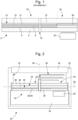
- the watch 30 comprises a case 32 having an upper opening 33, a glass 34 closing the upper opening, a movement 36, an analog display 38 driven by the movement, and an assembly 40 which is generally located between the movement and the display analog and which here advantageously itself forms the dial of the watch associated with the analog display, no cover plate of the assembly 40 being provided between this assembly and the analog display.
- Set 40 comprises a light sensor 42 comprising at least one photovoltaic cell and which is formed by a wafer or layer of semiconductor material 44 (also called semiconductor wafer or layer), at least one negative electrode 46 and at least one positive electrode 48 all located below the wafer or semiconductor layer.
- the assembly comprises or is fixed to a support 50 (depending on whether this support is considered to be part of the assembly or not), in particular by gluing.
- the wafer or layer of semiconductor material 44 is preferably a wafer or layer of silicon (Si).
- the semiconductor wafer or layer 44 has a lower region 45 which is doped to form zones facilitating the conduction of electrical charges towards said at least one negative electrode and said at least one positive electrode to which they are associated (a negatively doped zone, called n or N type, is connected to a negative electrode, while a positively doped zone, called p or P type, is connected to a positive electrode).
- a negatively doped zone called n or N type
- p or P type a positively doped zone
- a doped zone is, according to the usual notations in the field of semiconductors, either an N+ zone or a P+ zone, or an N++ zone or a P++ zone. To clearly indicate that we are considering a zone sufficiently doped to present significant electrical conduction, we mention 'conductive doped zone'.
- the wafer or layer of semiconductor material 44 has conductive doped zones over its entire lower part.
- the watch further comprises an antenna 20 arranged to be able to communicate through the crystal 34 with a communication device (not shown) which is external to the watch.
- the assembly 40 has a first part 52, in which are arranged entirely said at least one negative electrode 46 and said at least one positive electrode 48 and in which the light sensor 42 is therefore arranged, and a second part 54 without electrodes which is separated from the first part and of which a projection in the general plane 56 of said assembly (this general plane being perpendicular to the axis of rotation 58 of the needles forming the analog display 38) includes a projection of the antenna 20 in this general plane.
- the light sensor does not prevent the antenna from communicating with a communication device whose electromagnetic signals enter the watch through the crystal 34, because the antenna and the light sensor are arranged, in projection in the general plan of set 40, in separate regions. So that a user of the watch cannot distinguish the first part and the second part of the assembly 40 forming the dial, the wafer or layer of semiconductor material 44 extends, parallel to the general plane 56, in the first part 52 of the assembly 40, to form the light sensor 42, and also in the second part 54 of this assembly. Furthermore, according to the invention, all the electrodes of the light sensor are located below the wafer or semiconductor layer 44.
- the arrangement of the light sensor 42 does not generate any particular treatment of the upper surface of the wafer or layer of semiconductor material 44 and no deposit of material on this upper surface, which is uniform and presents a homogeneous opaque appearance to an observer.
- This observer cannot thus distinguish the presence of the light sensor by the presence of a structured upper layer, in particular transparent upper electrodes, as in the prior art.
- the semiconductor wafer or layer extends continuously from the first part 52 to the second part 54 and it forms a single and same semiconductor wafer or layer which extends at least partially in these first and second parts or, preferably, over the entire region of the assembly 40 which is visible to a user of the watch observing this assembly, forming a dial, through the glass 34.
- This last preferred variant makes it possible to obtain a dial with a homogeneous color and presenting the same uniform appearance for the user observing this assembly through the glass.
- the plate or layer of semiconductor material extends throughout the first part 52 and the second part 54 of the assembly 40, that is to say throughout the region of the light sensor 42 and all the region superimposed on the antenna 20.
- the assembly 40 further comprises at least one layer 60 which is transparent, semi-transparent or translucent and which is arranged above the semiconductor wafer or layer 44.
- the layer 60 is homogeneous and extends over the entire visible part of the assembly 40, forming the dial of the watch 30, for a user observing this assembly through the glass 34.
- this layer 60 forms an upper layer of the assembly 40 and has an upper surface which is uniform, at least in the region visible to a user observing this assembly through the glass.
- layer 60 is arranged so as to completely cover the wafer or semiconductor layer.
- this layer 60 does not alter the perfect homogeneity of color and the uniformity of appearance of the assembly 40 here forming the dial of the watch.
- the layer 60 is advantageously transparent, possibly with a slight coloring, and it determines, jointly with the wafer or semiconductor layer and any layers deposited on the latter, the color of the first part 52 and the second part 54 of the assembly 40 for a user observing this assembly through the glass 34, preferably from the entire region of this assembly visible to this user.
- the transparent, semi-transparent or translucent layer 60 darkens the color of the wafer or semiconductor layer, in particular it gives the assembly 40 an anthracite, midnight blue or black color for a user observing the assembly through ice.
- layer 60 darkens the color of set 40 and gives it a deep color with the most beautiful effect.
- the upper layer 60 determines the state of the upper surface of the assembly 40.
- the upper surface of the transparent, semi-transparent or translucent layer 60 can have a finish giving, at least in areas, a matte, brushed, satin or shiny appearance overall. In a variant, this upper surface has integral linear or radial brushing.
- the upper layer 60 of the assembly 40 is a layer of transparent varnish which is applied to the wafer or semiconductor layer 44.
- the assembly 40 may comprise at least one additional layer above the semiconductor wafer or layer. Such an additional layer may be a film forming a filter, an anti-reflection layer or a layer for diffusing light in transmission.
- the box 32 is formed at least mainly by one or more metallic material(s).
- the external parts of the box 32 are entirely metallic.
- this second embodiment is advantageously characterized by the fact that the positive electrodes and the negative electrodes are arranged under the wafer or layer of semiconductor material 44A.
- This second embodiment is essentially distinguished from the first embodiment by the fact that the antenna is included in the assembly or supported by the latter.
- an assembly 70 which forms a dial for a watch with an analog display and which comprises a light sensor 72 formed by at least one photovoltaic cell.
- the light sensor 72 is formed by a plate or layer of semiconductor material 44A, negative electrodes 78 and positive electrodes 79.
- the assembly 70 has a first part 52A, in which the electrodes are entirely arranged negative and positive electrodes, and a second part 54A which is, in projection in a general plane 56 of the assembly, separated from the first part.
- the second part is provided for the passage of electromagnetic signals coming from a communication device or generated by the antenna 80.
- the wafer or layer of semiconductor material 44A extends, parallel said general plan, in the first part 52A and the second part 54A of the set 70 which is a dial.
- the second part 54A of the assembly 70 comprises or supports, on a lower side of this assembly, an antenna 80.
- the wafer or layer of semiconductor material 44A does not does not present here any conductive doped zones in the second part of said assembly. It will be noted that the wafer or layer of semiconductor material 44A can be lightly doped partly or totally in the second part 54A of the assembly 70.
- the antenna 80 is located below the plate or layer of semiconductor material, so as to be invisible from the side of the upper surface 62 of the assembly, which is the visible surface of the dial formed by this assembly 70 a times the latter incorporated in a watch case to form a watch according to the invention.
- the second part 54A of the assembly 70 comprises the antenna 80, which is arranged below the semiconductor wafer or layer 44A.
- the antenna 80 is deposited on the same layer 82 as the electrodes 78 and 79 of the light sensor.
- the lower layer 82 is a passivation layer useful for the light sensor 72.
- the plurality of negative electrodes 78 and the plurality of positive electrodes 79 are all deposited lowerly on the passivation layer 82, which lowerly covers the semiconductor wafer or layer 44A, and are connected by openings provided in the passivation layer 82 respectively to a plurality of lower zones 74 doped N+ and to a plurality of lower zones 76 doped P+, these doped zones 74, 76 therefore being conductive.
- the antenna 80 is formed by the same material as the negative electrodes and the positive electrodes.
- the semiconductor wafer or layer is conductively doped in various regions of the first part of the assembly.
- the semiconductor wafer or layer is not doped conductively here in the second part 54A of the assembly.
- 'conductive doped' indicates 'doped so as to exhibit significant electrical conduction' and therefore 'conductive undoped' means 'undoped so as to exhibit significant electrical conduction' or equivalently 'non-doped or doped' so as to present an insignificant electrical conduction, that is to say very weak'.
- the wafer or semiconductor layer 44 can, in a variant, be lightly doped (that is to say n, N doped or p, P doped according to the usual terminology) .
- the wafer or semiconductor layer does not create a magnetic screen for the antenna by doping.
- the wafer or layer of semiconductor material 44A extends throughout the first part 52A and the entire second part 54A of the assembly 70.
- the wafer or layer of semiconductor material extends in projection over the entire upper surface 62 of the assembly 70.
- the wafer or layer of semiconductor material has texturing (micro-structuring) over its entire upper surface and at least one antireflection layer 84 is deposited on the wafer or layer of semiconductor material, so as to cover completely.
- the antireflection layer is deposited uniformly on the wafer or layer of semiconductor material.
- the assembly 70 may further comprise a light diffusion layer.
- all the layers deposited above the semiconductor wafer or layer 44A are deposited uniformly over the entire semiconductor wafer or layer.
- the treatment of at least one upper layer may not be uniform, but differentiated on purpose.
- the assembly 70 further comprises, as in the first embodiment, an upper layer 60 which is transparent or translucent and which determines, jointly with the wafer or layer of semiconductor material and the anti-reflective layer 84, the color of said first and second parts of the assembly on the side of the upper surface 62 of the assembly. In addition, it determines the state of this upper surface.
- the upper layer 60 is transparent and uniformly covers the entire upper surface 62 of the assembly 70.
- the assembly 70 is glued to a support 50 by means of a layer of glue 86.
- this support 50 is part of the assembly 70, or not.
- the assembly defines a module which forms a sundial, that is to say provided with at least one photovoltaic cell, and which also incorporates an antenna.
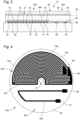
- FIG. 4 shows in section an assembly 70A which is a variant of the second embodiment.
- the section is parallel to the general plane of assembly 70A at the level of the electrodes of its light sensor. If we consider the support 50 and the glue layer 86 not included in the assembly or in the case where such a support is not provided, then the Figure 4 is a bottom view of the whole thing.
- This variant is particular by the arrangement of the plurality of negative electrodes 78A and the plurality of positive electrodes 79A, this arrangement making it possible to occupy in an optimized manner a semi-circle part or a truncated circle part of a disc having a hole 18 in its center for the passage of the axes of an analog display.
- the particular arrangement of the negative and positive electrodes, nested within each other, also makes it possible to have the negative contact pad 88, to which the negative electrodes 78A are connected, and the positive contact pad 89, to which are connected the positive electrodes 79A, one next to the other in the same radial zone of the assembly 70A, and thus having two adjacent contact areas which are close to each other, which facilitates the electrical connection to an electrical connector provided for the light sensor.
- the plurality of negative electrodes 78A and the plurality of positive electrodes 79A, the two contact pads 88 and 89 and the antenna 80A are deposited lowerly on the passivation layer 82 described above.
- the question of whether it is a plurality of negative electrodes and a plurality of positive electrodes or a single negative electrode and a single positive electrode each having a plurality of elongated arms, given that all the arms of the same polarity are connected to the same contact pad is a question of definition which has no consequences for the present invention.
- the antenna 80A is provided for high frequency communication, this antenna being formed by a single U-shaped track whose two ends are connected respectively to two contact pads 90 and 91 which are also deposited on the passivation layer 82, which in particular defines a rear mirror for the light sensor.
- the passivation layer extends over the entire wafer or semiconductor layer, which extends, in projection in the general plane of the assembly 70A, over this entire assembly.
- the light sensor occupies a first part 52A of the assembly and the antenna occupies a second part 54A of this assembly, distinct from the first part, these two parts constituting the entire assembly 70A.
- the second part of the assembly supports the antenna (a module forming this antenna) on a lower side of this assembly, this antenna being fixed to the assembly for example by gluing.
- the first part and the second part may have different shapes and that the electrodes may be arranged differently.
- the light sensor may be annular with the antenna arranged in the center.
- the first part of the assembly forms an annular structure and the second part of this assembly forms a central disk with a circular hole in its center.
- the second part may consist of a substantially rectangular or square portion which extends radially from the periphery of the assembly forming the dial, the first part of the assembly forming the part complementary to this radial portion.
Landscapes
- Physics & Mathematics (AREA)
- General Physics & Mathematics (AREA)
- Engineering & Computer Science (AREA)
- Power Engineering (AREA)
- Spectroscopy & Molecular Physics (AREA)
- Electric Clocks (AREA)
Applications Claiming Priority (1)
| Application Number | Priority Date | Filing Date | Title |
|---|---|---|---|
| EP22193119 | 2022-08-31 |
Publications (2)
| Publication Number | Publication Date |
|---|---|
| EP4332693A1 true EP4332693A1 (de) | 2024-03-06 |
| EP4332693B1 EP4332693B1 (de) | 2025-04-02 |
Family
ID=83151664
Family Applications (1)
| Application Number | Title | Priority Date | Filing Date |
|---|---|---|---|
| EP23184951.4A Active EP4332693B1 (de) | 2022-08-31 | 2023-07-12 | Uhr mit einem lichtsensor und einer antenne |
Country Status (3)
| Country | Link |
|---|---|
| US (1) | US20240069495A1 (de) |
| EP (1) | EP4332693B1 (de) |
| CN (1) | CN117631519A (de) |
Citations (2)
| Publication number | Priority date | Publication date | Assignee | Title |
|---|---|---|---|---|
| US20150268639A1 (en) * | 2014-03-18 | 2015-09-24 | Casio Computer Co., Ltd. | Electronic device |
| JP2019060847A (ja) | 2017-09-26 | 2019-04-18 | セイコーエプソン株式会社 | 電子時計 |
-
2023
- 2023-07-12 EP EP23184951.4A patent/EP4332693B1/de active Active
- 2023-07-21 US US18/356,561 patent/US20240069495A1/en active Pending
- 2023-08-31 CN CN202311120106.0A patent/CN117631519A/zh active Pending
Patent Citations (2)
| Publication number | Priority date | Publication date | Assignee | Title |
|---|---|---|---|---|
| US20150268639A1 (en) * | 2014-03-18 | 2015-09-24 | Casio Computer Co., Ltd. | Electronic device |
| JP2019060847A (ja) | 2017-09-26 | 2019-04-18 | セイコーエプソン株式会社 | 電子時計 |
Also Published As
| Publication number | Publication date |
|---|---|
| CN117631519A (zh) | 2024-03-01 |
| EP4332693B1 (de) | 2025-04-02 |
| US20240069495A1 (en) | 2024-02-29 |
Similar Documents
| Publication | Publication Date | Title |
|---|---|---|
| EP2339647B1 (de) | Photodetektor mit Plasmonstruktur | |
| EP3238254B1 (de) | Farbbildsensor mit weissen pixeln und farbpixeln | |
| FR2954854A1 (fr) | Photodetecteur a structure plasmon | |
| EP2786412B1 (de) | Optische detektoreinheit | |
| EP2840617B1 (de) | BSI-Fotodiode mit hoher Quanteneffizienz | |
| EP3660930A1 (de) | Herstellungsverfahren einer fotodiodenmatrix auf germaniumbasis und mit schwachem dunkelstrom | |
| EP3836214A1 (de) | Lichtsensor | |
| EP2865017A1 (de) | Halbleiterstruktur mit einem absorbierenden bereich in einer fokussierungskavität | |
| EP4332693B1 (de) | Uhr mit einem lichtsensor und einer antenne | |
| EP2276072B1 (de) | Photodetektorelement | |
| CH720001A2 (fr) | Montre munie d'un capteur de lumière et d'une antenne. | |
| EP4421568A1 (de) | Uhr mit einer transparenten oder transluzenten dekorativen struktur, insbesondere einer halbemail | |
| EP4390475A1 (de) | Polarisatorfilter und polarimetrischer bildsensor mit einem solchen filter | |
| EP2432033A2 (de) | Bispektraler Mehrschichtdetektor mit Fotodioden | |
| FR2929478A1 (fr) | Capteur d'image a sensibilite amelioree | |
| CH691635A5 (fr) | Cadran formé d'une cellule solaire, notamment pour pièce d'horlogerie. | |
| WO2019149384A1 (fr) | Cadran pour pièce d'horlogerie et son procédé de fabrication | |
| EP4365957A1 (de) | Anordnung aus photovoltaischen zellen und zell- und elektronischer schaltung mit einem messbereich | |
| EP0070234A2 (de) | Optoelektronische Halbleiterstruktur mit einem Sende- und Empfangsteil sowie eine Vorrichtung zum Regeln einer Lumineszenzdiode | |
| EP0902339A1 (de) | Ein aus einer Solarzelle bestehendes Zifferblatt, insbesondere für eine Uhr | |
| EP1113503B1 (de) | Verfahren zur Herstellung einer Farbigen photovoltaischen Zelle, insbesondere für das Ziffernblatt einer Uhr | |
| WO2014060479A1 (fr) | Capteur d'image a efficacite quantique amelioree dans les grandes longueurs d'onde | |
| EP1174756B1 (de) | Anzeigeeinheit mit einer elektrooptischen und einer photovoltaischen Zelle | |
| CH720538A2 (fr) | Montre munie d'une structure décorative transparente et/ou translucide, notamment d'un émail plique-à-jour | |
| EP3208854A1 (de) | Photodiodenstruktur, bestandteil und herstellungsverfahren einer solchen photodiodenstruktur |
Legal Events
| Date | Code | Title | Description |
|---|---|---|---|
| PUAI | Public reference made under article 153(3) epc to a published international application that has entered the european phase |
Free format text: ORIGINAL CODE: 0009012 |
|
| STAA | Information on the status of an ep patent application or granted ep patent |
Free format text: STATUS: THE APPLICATION HAS BEEN PUBLISHED |
|
| AK | Designated contracting states |
Kind code of ref document: A1 Designated state(s): AL AT BE BG CH CY CZ DE DK EE ES FI FR GB GR HR HU IE IS IT LI LT LU LV MC ME MK MT NL NO PL PT RO RS SE SI SK SM TR |
|
| STAA | Information on the status of an ep patent application or granted ep patent |
Free format text: STATUS: REQUEST FOR EXAMINATION WAS MADE |
|
| 17P | Request for examination filed |
Effective date: 20240906 |
|
| RBV | Designated contracting states (corrected) |
Designated state(s): AL AT BE BG CH CY CZ DE DK EE ES FI FR GB GR HR HU IE IS IT LI LT LU LV MC ME MK MT NL NO PL PT RO RS SE SI SK SM TR |
|
| REG | Reference to a national code |
Ref country code: DE Ref legal event code: R079 Free format text: PREVIOUS MAIN CLASS: G04C0010020000 Ipc: G04G0017040000 Ref document number: 602023002698 Country of ref document: DE |
|
| GRAP | Despatch of communication of intention to grant a patent |
Free format text: ORIGINAL CODE: EPIDOSNIGR1 |
|
| STAA | Information on the status of an ep patent application or granted ep patent |
Free format text: STATUS: GRANT OF PATENT IS INTENDED |
|
| RIC1 | Information provided on ipc code assigned before grant |
Ipc: G04C 10/02 20060101ALI20241223BHEP Ipc: G04G 19/10 20060101ALI20241223BHEP Ipc: G04G 17/04 20060101AFI20241223BHEP |
|
| INTG | Intention to grant announced |
Effective date: 20250114 |
|
| GRAS | Grant fee paid |
Free format text: ORIGINAL CODE: EPIDOSNIGR3 |
|
| GRAA | (expected) grant |
Free format text: ORIGINAL CODE: 0009210 |
|
| STAA | Information on the status of an ep patent application or granted ep patent |
Free format text: STATUS: THE PATENT HAS BEEN GRANTED |
|
| P01 | Opt-out of the competence of the unified patent court (upc) registered |
Free format text: CASE NUMBER: APP_6838/2025 Effective date: 20250210 |
|
| AK | Designated contracting states |
Kind code of ref document: B1 Designated state(s): AL AT BE BG CH CY CZ DE DK EE ES FI FR GB GR HR HU IE IS IT LI LT LU LV MC ME MK MT NL NO PL PT RO RS SE SI SK SM TR |
|
| REG | Reference to a national code |
Ref country code: GB Ref legal event code: FG4D Free format text: NOT ENGLISH |
|
| REG | Reference to a national code |
Ref country code: CH Ref legal event code: EP |
|
| REG | Reference to a national code |
Ref country code: DE Ref legal event code: R096 Ref document number: 602023002698 Country of ref document: DE |
|
| REG | Reference to a national code |
Ref country code: IE Ref legal event code: FG4D Free format text: LANGUAGE OF EP DOCUMENT: FRENCH |
|
| PGFP | Annual fee paid to national office [announced via postgrant information from national office to epo] |
Ref country code: FR Payment date: 20250620 Year of fee payment: 3 |
|
| REG | Reference to a national code |
Ref country code: NL Ref legal event code: MP Effective date: 20250402 |
|
| PG25 | Lapsed in a contracting state [announced via postgrant information from national office to epo] |
Ref country code: NL Free format text: LAPSE BECAUSE OF FAILURE TO SUBMIT A TRANSLATION OF THE DESCRIPTION OR TO PAY THE FEE WITHIN THE PRESCRIBED TIME-LIMIT Effective date: 20250402 |
|
| REG | Reference to a national code |
Ref country code: AT Ref legal event code: MK05 Ref document number: 1781856 Country of ref document: AT Kind code of ref document: T Effective date: 20250402 |
|
| PG25 | Lapsed in a contracting state [announced via postgrant information from national office to epo] |
Ref country code: FI Free format text: LAPSE BECAUSE OF FAILURE TO SUBMIT A TRANSLATION OF THE DESCRIPTION OR TO PAY THE FEE WITHIN THE PRESCRIBED TIME-LIMIT Effective date: 20250402 Ref country code: ES Free format text: LAPSE BECAUSE OF FAILURE TO SUBMIT A TRANSLATION OF THE DESCRIPTION OR TO PAY THE FEE WITHIN THE PRESCRIBED TIME-LIMIT Effective date: 20250402 Ref country code: PT Free format text: LAPSE BECAUSE OF FAILURE TO SUBMIT A TRANSLATION OF THE DESCRIPTION OR TO PAY THE FEE WITHIN THE PRESCRIBED TIME-LIMIT Effective date: 20250804 |
|
| PGFP | Annual fee paid to national office [announced via postgrant information from national office to epo] |
Ref country code: DE Payment date: 20250620 Year of fee payment: 3 |
|
| REG | Reference to a national code |
Ref country code: LT Ref legal event code: MG9D |
|
| PG25 | Lapsed in a contracting state [announced via postgrant information from national office to epo] |
Ref country code: NO Free format text: LAPSE BECAUSE OF FAILURE TO SUBMIT A TRANSLATION OF THE DESCRIPTION OR TO PAY THE FEE WITHIN THE PRESCRIBED TIME-LIMIT Effective date: 20250702 Ref country code: GR Free format text: LAPSE BECAUSE OF FAILURE TO SUBMIT A TRANSLATION OF THE DESCRIPTION OR TO PAY THE FEE WITHIN THE PRESCRIBED TIME-LIMIT Effective date: 20250703 |
|
| PG25 | Lapsed in a contracting state [announced via postgrant information from national office to epo] |
Ref country code: PL Free format text: LAPSE BECAUSE OF FAILURE TO SUBMIT A TRANSLATION OF THE DESCRIPTION OR TO PAY THE FEE WITHIN THE PRESCRIBED TIME-LIMIT Effective date: 20250402 |
|
| PG25 | Lapsed in a contracting state [announced via postgrant information from national office to epo] |
Ref country code: BG Free format text: LAPSE BECAUSE OF FAILURE TO SUBMIT A TRANSLATION OF THE DESCRIPTION OR TO PAY THE FEE WITHIN THE PRESCRIBED TIME-LIMIT Effective date: 20250402 |
|
| PG25 | Lapsed in a contracting state [announced via postgrant information from national office to epo] |
Ref country code: HR Free format text: LAPSE BECAUSE OF FAILURE TO SUBMIT A TRANSLATION OF THE DESCRIPTION OR TO PAY THE FEE WITHIN THE PRESCRIBED TIME-LIMIT Effective date: 20250402 |
|
| PG25 | Lapsed in a contracting state [announced via postgrant information from national office to epo] |
Ref country code: AT Free format text: LAPSE BECAUSE OF FAILURE TO SUBMIT A TRANSLATION OF THE DESCRIPTION OR TO PAY THE FEE WITHIN THE PRESCRIBED TIME-LIMIT Effective date: 20250402 |
|
| PG25 | Lapsed in a contracting state [announced via postgrant information from national office to epo] |
Ref country code: RS Free format text: LAPSE BECAUSE OF FAILURE TO SUBMIT A TRANSLATION OF THE DESCRIPTION OR TO PAY THE FEE WITHIN THE PRESCRIBED TIME-LIMIT Effective date: 20250702 |
|
| PG25 | Lapsed in a contracting state [announced via postgrant information from national office to epo] |
Ref country code: IS Free format text: LAPSE BECAUSE OF FAILURE TO SUBMIT A TRANSLATION OF THE DESCRIPTION OR TO PAY THE FEE WITHIN THE PRESCRIBED TIME-LIMIT Effective date: 20250802 |
|
| PG25 | Lapsed in a contracting state [announced via postgrant information from national office to epo] |
Ref country code: LV Free format text: LAPSE BECAUSE OF FAILURE TO SUBMIT A TRANSLATION OF THE DESCRIPTION OR TO PAY THE FEE WITHIN THE PRESCRIBED TIME-LIMIT Effective date: 20250402 |
|
| REG | Reference to a national code |
Ref country code: DE Ref legal event code: R097 Ref document number: 602023002698 Country of ref document: DE |
|
| PG25 | Lapsed in a contracting state [announced via postgrant information from national office to epo] |
Ref country code: DK Free format text: LAPSE BECAUSE OF FAILURE TO SUBMIT A TRANSLATION OF THE DESCRIPTION OR TO PAY THE FEE WITHIN THE PRESCRIBED TIME-LIMIT Effective date: 20250402 Ref country code: SM Free format text: LAPSE BECAUSE OF FAILURE TO SUBMIT A TRANSLATION OF THE DESCRIPTION OR TO PAY THE FEE WITHIN THE PRESCRIBED TIME-LIMIT Effective date: 20250402 |
|
| PG25 | Lapsed in a contracting state [announced via postgrant information from national office to epo] |
Ref country code: CZ Free format text: LAPSE BECAUSE OF FAILURE TO SUBMIT A TRANSLATION OF THE DESCRIPTION OR TO PAY THE FEE WITHIN THE PRESCRIBED TIME-LIMIT Effective date: 20250402 |
|
| PG25 | Lapsed in a contracting state [announced via postgrant information from national office to epo] |
Ref country code: EE Free format text: LAPSE BECAUSE OF FAILURE TO SUBMIT A TRANSLATION OF THE DESCRIPTION OR TO PAY THE FEE WITHIN THE PRESCRIBED TIME-LIMIT Effective date: 20250402 |
|
| PG25 | Lapsed in a contracting state [announced via postgrant information from national office to epo] |
Ref country code: SK Free format text: LAPSE BECAUSE OF FAILURE TO SUBMIT A TRANSLATION OF THE DESCRIPTION OR TO PAY THE FEE WITHIN THE PRESCRIBED TIME-LIMIT Effective date: 20250402 |
|
| PG25 | Lapsed in a contracting state [announced via postgrant information from national office to epo] |
Ref country code: IT Free format text: LAPSE BECAUSE OF FAILURE TO SUBMIT A TRANSLATION OF THE DESCRIPTION OR TO PAY THE FEE WITHIN THE PRESCRIBED TIME-LIMIT Effective date: 20250402 |
|
| PLBE | No opposition filed within time limit |
Free format text: ORIGINAL CODE: 0009261 |
|
| STAA | Information on the status of an ep patent application or granted ep patent |
Free format text: STATUS: NO OPPOSITION FILED WITHIN TIME LIMIT |
|
| REG | Reference to a national code |
Ref country code: CH Ref legal event code: L10 Free format text: ST27 STATUS EVENT CODE: U-0-0-L10-L00 (AS PROVIDED BY THE NATIONAL OFFICE) Effective date: 20260211 |
|
| PG25 | Lapsed in a contracting state [announced via postgrant information from national office to epo] |
Ref country code: RO Free format text: LAPSE BECAUSE OF FAILURE TO SUBMIT A TRANSLATION OF THE DESCRIPTION OR TO PAY THE FEE WITHIN THE PRESCRIBED TIME-LIMIT Effective date: 20250402 |
|
| 26N | No opposition filed |
Effective date: 20260105 |
|
| PG25 | Lapsed in a contracting state [announced via postgrant information from national office to epo] |
Ref country code: LU Free format text: LAPSE BECAUSE OF NON-PAYMENT OF DUE FEES Effective date: 20250712 |
|
| REG | Reference to a national code |
Ref country code: BE Ref legal event code: MM Effective date: 20250731 |
|
| PG25 | Lapsed in a contracting state [announced via postgrant information from national office to epo] |
Ref country code: BE Free format text: LAPSE BECAUSE OF NON-PAYMENT OF DUE FEES Effective date: 20250731 |