EP4332973B1 - Procédé de programmation d'un dispositif de mémoire multi-plan - Google Patents
Procédé de programmation d'un dispositif de mémoire multi-plan Download PDFInfo
- Publication number
- EP4332973B1 EP4332973B1 EP24152294.5A EP24152294A EP4332973B1 EP 4332973 B1 EP4332973 B1 EP 4332973B1 EP 24152294 A EP24152294 A EP 24152294A EP 4332973 B1 EP4332973 B1 EP 4332973B1
- Authority
- EP
- European Patent Office
- Prior art keywords
- planes
- controller
- plane
- program
- failed
- Prior art date
- Legal status (The legal status is an assumption and is not a legal conclusion. Google has not performed a legal analysis and makes no representation as to the accuracy of the status listed.)
- Active
Links
Images



Classifications
-
- G—PHYSICS
- G11—INFORMATION STORAGE
- G11C—STATIC STORES
- G11C16/00—Erasable programmable read-only memories
- G11C16/02—Erasable programmable read-only memories electrically programmable
- G11C16/06—Auxiliary circuits, e.g. for writing into memory
- G11C16/10—Programming or data input circuits
-
- G—PHYSICS
- G06—COMPUTING OR CALCULATING; COUNTING
- G06F—ELECTRIC DIGITAL DATA PROCESSING
- G06F3/00—Input arrangements for transferring data to be processed into a form capable of being handled by the computer; Output arrangements for transferring data from processing unit to output unit, e.g. interface arrangements
- G06F3/06—Digital input from, or digital output to, record carriers, e.g. RAID, emulated record carriers or networked record carriers
- G06F3/0601—Interfaces specially adapted for storage systems
- G06F3/0602—Interfaces specially adapted for storage systems specifically adapted to achieve a particular effect
- G06F3/0604—Improving or facilitating administration, e.g. storage management
- G06F3/0607—Improving or facilitating administration, e.g. storage management by facilitating the process of upgrading existing storage systems, e.g. for improving compatibility between host and storage device
-
- G—PHYSICS
- G06—COMPUTING OR CALCULATING; COUNTING
- G06F—ELECTRIC DIGITAL DATA PROCESSING
- G06F12/00—Accessing, addressing or allocating within memory systems or architectures
- G06F12/02—Addressing or allocation; Relocation
- G06F12/0223—User address space allocation, e.g. contiguous or non contiguous base addressing
- G06F12/023—Free address space management
- G06F12/0238—Memory management in non-volatile memory, e.g. resistive RAM or ferroelectric memory
- G06F12/0246—Memory management in non-volatile memory, e.g. resistive RAM or ferroelectric memory in block erasable memory, e.g. flash memory
-
- G—PHYSICS
- G06—COMPUTING OR CALCULATING; COUNTING
- G06F—ELECTRIC DIGITAL DATA PROCESSING
- G06F3/00—Input arrangements for transferring data to be processed into a form capable of being handled by the computer; Output arrangements for transferring data from processing unit to output unit, e.g. interface arrangements
- G06F3/06—Digital input from, or digital output to, record carriers, e.g. RAID, emulated record carriers or networked record carriers
- G06F3/0601—Interfaces specially adapted for storage systems
- G06F3/0628—Interfaces specially adapted for storage systems making use of a particular technique
- G06F3/0655—Vertical data movement, i.e. input-output transfer; data movement between one or more hosts and one or more storage devices
- G06F3/0658—Controller construction arrangements
-
- G—PHYSICS
- G06—COMPUTING OR CALCULATING; COUNTING
- G06F—ELECTRIC DIGITAL DATA PROCESSING
- G06F3/00—Input arrangements for transferring data to be processed into a form capable of being handled by the computer; Output arrangements for transferring data from processing unit to output unit, e.g. interface arrangements
- G06F3/06—Digital input from, or digital output to, record carriers, e.g. RAID, emulated record carriers or networked record carriers
- G06F3/0601—Interfaces specially adapted for storage systems
- G06F3/0668—Interfaces specially adapted for storage systems adopting a particular infrastructure
- G06F3/0671—In-line storage system
- G06F3/0673—Single storage device
- G06F3/0679—Non-volatile semiconductor memory device, e.g. flash memory, one time programmable memory [OTP]
-
- G—PHYSICS
- G11—INFORMATION STORAGE
- G11C—STATIC STORES
- G11C11/00—Digital stores characterised by the use of particular electric or magnetic storage elements; Storage elements therefor
- G11C11/56—Digital stores characterised by the use of particular electric or magnetic storage elements; Storage elements therefor using storage elements with more than two stable states represented by steps, e.g. of voltage, current, phase, frequency
- G11C11/5621—Digital stores characterised by the use of particular electric or magnetic storage elements; Storage elements therefor using storage elements with more than two stable states represented by steps, e.g. of voltage, current, phase, frequency using charge storage in a floating gate
- G11C11/5628—Programming or writing circuits; Data input circuits
-
- G—PHYSICS
- G11—INFORMATION STORAGE
- G11C—STATIC STORES
- G11C11/00—Digital stores characterised by the use of particular electric or magnetic storage elements; Storage elements therefor
- G11C11/56—Digital stores characterised by the use of particular electric or magnetic storage elements; Storage elements therefor using storage elements with more than two stable states represented by steps, e.g. of voltage, current, phase, frequency
- G11C11/5671—Digital stores characterised by the use of particular electric or magnetic storage elements; Storage elements therefor using storage elements with more than two stable states represented by steps, e.g. of voltage, current, phase, frequency using charge trapping in an insulator
-
- G—PHYSICS
- G11—INFORMATION STORAGE
- G11C—STATIC STORES
- G11C16/00—Erasable programmable read-only memories
- G11C16/02—Erasable programmable read-only memories electrically programmable
- G11C16/04—Erasable programmable read-only memories electrically programmable using variable threshold transistors, e.g. FAMOS
- G11C16/0483—Erasable programmable read-only memories electrically programmable using variable threshold transistors, e.g. FAMOS comprising cells having several storage transistors connected in series
-
- G—PHYSICS
- G11—INFORMATION STORAGE
- G11C—STATIC STORES
- G11C16/00—Erasable programmable read-only memories
- G11C16/02—Erasable programmable read-only memories electrically programmable
- G11C16/06—Auxiliary circuits, e.g. for writing into memory
- G11C16/08—Address circuits; Decoders; Word-line control circuits
-
- G—PHYSICS
- G11—INFORMATION STORAGE
- G11C—STATIC STORES
- G11C16/00—Erasable programmable read-only memories
- G11C16/02—Erasable programmable read-only memories electrically programmable
- G11C16/06—Auxiliary circuits, e.g. for writing into memory
- G11C16/24—Bit-line control circuits
-
- G—PHYSICS
- G11—INFORMATION STORAGE
- G11C—STATIC STORES
- G11C16/00—Erasable programmable read-only memories
- G11C16/02—Erasable programmable read-only memories electrically programmable
- G11C16/06—Auxiliary circuits, e.g. for writing into memory
- G11C16/26—Sensing or reading circuits; Data output circuits
-
- G—PHYSICS
- G11—INFORMATION STORAGE
- G11C—STATIC STORES
- G11C16/00—Erasable programmable read-only memories
- G11C16/02—Erasable programmable read-only memories electrically programmable
- G11C16/06—Auxiliary circuits, e.g. for writing into memory
- G11C16/34—Determination of programming status, e.g. threshold voltage, overprogramming or underprogramming, retention
- G11C16/3436—Arrangements for verifying correct programming or erasure
- G11C16/3454—Arrangements for verifying correct programming or for detecting overprogrammed cells
- G11C16/3459—Circuits or methods to verify correct programming of nonvolatile memory cells
-
- G—PHYSICS
- G11—INFORMATION STORAGE
- G11C—STATIC STORES
- G11C29/00—Checking stores for correct operation ; Subsequent repair; Testing stores during standby or offline operation
- G11C29/04—Detection or location of defective memory elements, e.g. cell constructio details, timing of test signals
- G11C29/50—Marginal testing, e.g. race, voltage or current testing
- G11C29/50004—Marginal testing, e.g. race, voltage or current testing of threshold voltage
-
- G—PHYSICS
- G11—INFORMATION STORAGE
- G11C—STATIC STORES
- G11C29/00—Checking stores for correct operation ; Subsequent repair; Testing stores during standby or offline operation
- G11C29/70—Masking faults in memories by using spares or by reconfiguring
- G11C29/88—Masking faults in memories by using spares or by reconfiguring with partially good memories
- G11C29/883—Masking faults in memories by using spares or by reconfiguring with partially good memories using a single defective memory device with reduced capacity, e.g. half capacity
-
- G—PHYSICS
- G11—INFORMATION STORAGE
- G11C—STATIC STORES
- G11C5/00—Details of stores covered by group G11C11/00
- G11C5/02—Disposition of storage elements, e.g. in the form of a matrix array
- G11C5/025—Geometric lay-out considerations of storage- and peripheral-blocks in a semiconductor storage device
-
- G—PHYSICS
- G11—INFORMATION STORAGE
- G11C—STATIC STORES
- G11C7/00—Arrangements for writing information into, or reading information out from, a digital store
- G11C7/10—Input/output [I/O] data interface arrangements, e.g. I/O data control circuits, I/O data buffers
- G11C7/1006—Data managing, e.g. manipulating data before writing or reading out, data bus switches or control circuits therefor
-
- G—PHYSICS
- G11—INFORMATION STORAGE
- G11C—STATIC STORES
- G11C8/00—Arrangements for selecting an address in a digital store
- G11C8/12—Group selection circuits, e.g. for memory block selection, chip selection, array selection
-
- G—PHYSICS
- G11—INFORMATION STORAGE
- G11C—STATIC STORES
- G11C29/00—Checking stores for correct operation ; Subsequent repair; Testing stores during standby or offline operation
- G11C29/04—Detection or location of defective memory elements, e.g. cell constructio details, timing of test signals
- G11C2029/0409—Online test
-
- G—PHYSICS
- G11—INFORMATION STORAGE
- G11C—STATIC STORES
- G11C2211/00—Indexing scheme relating to digital stores characterized by the use of particular electric or magnetic storage elements; Storage elements therefor
- G11C2211/56—Indexing scheme relating to G11C11/56 and sub-groups for features not covered by these groups
- G11C2211/564—Miscellaneous aspects
- G11C2211/5642—Multilevel memory with buffers, latches, registers at input or output
-
- G—PHYSICS
- G11—INFORMATION STORAGE
- G11C—STATIC STORES
- G11C2211/00—Indexing scheme relating to digital stores characterized by the use of particular electric or magnetic storage elements; Storage elements therefor
- G11C2211/56—Indexing scheme relating to G11C11/56 and sub-groups for features not covered by these groups
- G11C2211/564—Miscellaneous aspects
- G11C2211/5644—Multilevel memory comprising counting devices
Definitions
- the invention relates to memory control, and in particular, to a method of programming a multi-plane memory device.
- Non-volatile memory has been used extensively in personal computers, telecommunications, consumer electronics and other fields. Electrically erasable programmable read only memory (EEPROM) and flash memory are among the most widely employed non-volatile memory.
- EEPROM Electrically erasable programmable read only memory
- flash memory is among the most widely employed non-volatile memory.
- the US10134474B1 describes an apparatus with a first and second plane of memory cells, a buffer and controller that an independent state completion for each plane during flash memory programming.
- the US20170352430A1 describes a non-volatile memory with customized control of injection type of disturb during program verify for improved program performance.
- the US20190066736A1 describes a NAND cell encoding to improve data integrity by obtaining the temperature and modify the cell encoding based on the obtained temperature.
- Memory devices may be classified into a single-plane type and a multi-plane type in accordance with the structural configuration of memory arrays.
- the single-plane type memory device includes memory arrays organized into a single plane
- the multi-plane type memory device includes memory arrays organized into a plurality of planes.
- two or more memory planes may be programmed simultaneously to enhance the programming efficiency.
- both the normal memory planes and defective memory planes will be repeatedly programmed in an attempt to program data into the defective memory planes, decreasing the programming speed, reducing the programming efficiency, and increasing program disturbance in the normal memory plane.
- a memory device includes a plurality of planes, a row driver and a controller.
- a method of programming the memory device includes in a program operation, the row driver applying a program pulse to a plurality of memory cells of a first plane of the plurality of planes; after the row driver applies the program pulse to the plurality of memory cells, the controller verifying if the plurality of memory cells have reached a predetermined program state; and if a preset number of the plurality of memory cells have failed to reach the predetermined program state after the plurality of memory cells have been verified for a predetermined number of times, the controller disabling the first plane.
- embodiments of the invention will be described with reference to a 2-dimentional NAND flash device, it will be understood that embodiments of the present inventive concept are not limited thereto to this configuration but are also applicable to a 3-dimentional NAND flash memory device.
- the invention is applicable to other nonvolatile memory devices, such as an electrically erasable and programmable read only memory (EEPROM), a NOR flash memory, a phase-change RAM (PRAM), a magnetic RAM (MRAM), a resistive RAM (RRAM), a ferroelectric RAM (FRAM), and the like, without departing from the scope of the present invention.
- EEPROM electrically erasable and programmable read only memory
- NOR flash memory NOR flash memory
- PRAM phase-change RAM
- MRAM magnetic RAM
- RRAM resistive RAM
- FRAM ferroelectric RAM
- FIG. 1 is a block diagram of a memory device 1 according to an embodiment of the invention.
- the memory device 1 has a dual-plane structure, and may include a controller 10, a voltage generation circuit 11, a row decoder 12, column drivers 131, 132 and planes 141, 142. While the dual-plane structure is used in the embodiment, it should be appreciated that other numbers of planes may also be adopted within the scope of the invention.
- the planes 141, 142 may be programmed simultaneously. After programming, if the plane 141 or the plane 142 is verified as failed for a predetermined number of times, the row driver 12 may disable the failed plane 141 or 142 from subsequent programming. The disablement of the failed plane reduces the time spent in an attempt to program the same, and reduce program disturbance in the operating plane.
- the controller 10 may be coupled to the voltage generation circuit 11 and the column drivers 131, 132.
- the voltage generation circuit 11 may be coupled to the row driver 12.
- the row driver 12 may be coupled to the plane 142 via a string select line SSL2, word lines WL2(1) to WL2(N) and a ground select line GSL2.
- the column driver 132 may be coupled to the plane 142 via bit lines BL2(1) to BL2(M).
- Each of the planes 141, 142 may contain a plurality of blocks, each block may contain a plurality of pages, and each page may contain an array of memory cells.
- the array of memory cells in the plane 141 may be addressed by the word lines WL1 (1) to WL1(N) and the bit lines BL1(1) to BL1(M), and the array of memory cells in the plane 142 may be addressed by the word lines WL2(1) to WL2(N) and the bit lines BL2(1) to BL2(M).
- the controller 10 may communicate with an external host to receive data for storage in the planes 141, 142 and to transmit data fetched from the planes 141, 142.
- the controller 10 may receive commands, addresses or data from the external host and generate column address signals Scadrl, Scadr2, a row address signal Sradr and a voltage control signal Svc.
- the voltage generation circuit 11 may generate voltages for read, program, erasure and verification operations in response to the voltage control signal Svc from the controller 10. The voltages generated by the voltage generation circuit 11 may exceed a supply voltage provided to the memory device 1.
- the row driver 12 may operate in response to the row address signal Sradr from the controller 10 to select word lines for the read, program, erasure and verification operations.
- the column drivers 131, 132 may operate in response to the column address signals Scadrl, Scadr2 from the controller 10 to generate bit line signals to select bit lines for the read, program, erasure and verification operations.
- the voltage generation circuit 11 may generate a program voltage (e.g., 20V) and a program pass voltage (e.g., 10V) using the supply voltage (e.g., 3.3V)
- the row driver 12 may apply a program pulse having the magnitude of the program voltage to selected word lines, apply the program pass voltage to unselected word lines, apply the supply voltage to the string select lines SSL1, SSL2 and apply the ground voltage to the ground select lines GSL1, GSL2, and the column drivers 131, 132 may apply a ground voltage (e.g., 0V) to selected bit lines, and apply the supply voltage to unselected bit lines.
- the voltage generation circuit 11 may generate an appropriate verification voltage
- the row driver 12 may apply the appropriate verification voltage to selected word lines, apply the supply voltage to the string select lines SSL1, SSL2 and apply the supply voltage to the ground select lines GSL1, GSL2, and the column drivers 131, 132 may apply the ground voltage to unselected bit lines, and apply the supply voltage to selected bit lines of the planes 141, 142 to read data from selected memory cells on the selected bit lines, respectively. If data read is incorrect, the controller 10 may verify the selected memory cell as failed, and if data read is correct, the controller 10 may verify the selected memory cell as passed.
- FIG. 2 is a schematic diagram of a page in the planes 141, 142.
- the page may include memory cells C(1,1) to C(M,N), string select cells Css(1) to Css(M) and ground select cells Cgs(1) to Cgs(M).
- the memory cells C(1,1) to C(M,N) may be floating-gate transistors or charge-trapping transistors, and each of the memory cells C(1,1) to C(M,N), the string select cells Css(1) to Css(M) and the ground select cells Cgs(1) to Cgs(M) may include a control terminal, a first terminal and a second terminal.
- a string select line SSLn may be coupled to the control terminals of the string select cells Css(1) to Css(M), and the bit lines BL(1) to BL(M) may be respectively coupled to the first terminals of the string select cells Css(1) to Css(M).
- the memory cells C(1,1) to C(M,N) may be arranged into rows of memory cells coupled to the respective word lines WL(1) to WL(N).
- the word lines WL(1) to WL(N) may be coupled to the control terminals of the memory cells C(1,1) to C(M,1) of the first row to the control terminals of the memory cells C(1,N) to C(M,N) of the Nth row, respectively, and the first terminals of the memory cells C(1,1) to C(M,1) may be respectively coupled to the second terminals of the string select cells Css(1) to Css(M).
- a ground select line GSLn may be coupled to the control terminals of the ground select cells Cgs(1) to Cgs(M), the first terminals of the ground select cells Cgs(1) to Cgs(M) may be respectively coupled to the second terminals of the memory cells C(1,N) to C(M,N), and the second terminals of the ground select cells Cgs(1) to Cgs(M) may be coupled to ground terminals.
- the ground terminals may provide the ground voltage.
- the memory cells C(1,1) to C(M,N) may be of a single-level cell (SLC) type, a multi-level cell (MLC) type, a triple-level cell (TLC) type, a quad-level cell (QLC) type, a penta-level cell (PLC) type, or a higher-level type.
- the Q possible data states may include an erase state S(0) and program states S(1) to S(Q-1), with the program state S(1) being the lowest program state and the program state S(Q-1) being the highest program state.
- a TLC may be programmed into one of 8 possible data states, with the program state S(1) being the lowest program state and the program state S(7) being the highest program state.
- the memory cells C(1,1) to C(M,N) may be initially set in the erase state S(0), and later, a series of program-verification operations may be performed on the memory cells C(1,1) to C(M,N) to program the same into respective target program states.
- the series of program-verification operations may start from the lowest program state S(1) and proceed to higher program states until the threshold voltages of selected memory cells reach respective verification voltage levels of respective target program states.
- the verification voltages may be selected as the minimum threshold voltages of threshold voltage distribution curves of the program states S(1) to S(Q-1), respectively.
- Each program-verification operation may include a program operation and a subsequent verification operation.
- some of the memory cells C(1,1) to C(M,N) may be selected and programmed into a program state in a row-by-row manner from the first row to the Nth row, or from the Nth row to the first row.
- the controller 10 may verify whether the selected memory cells have reached the program states in the row-by-row manner from the first row to the Nth row, or from the Nth row to the first row. In this fashion, the memory cells C(1,1) to C(M,N) may be programmed into the respective target program states.
- FIG. 3 is a block diagram of the column drivers 131, 132 and the controller 10.
- Each of the column drivers 131, 132 may include page buffers 301 to 30n, fail bit counters 321 to 32n and column decoders 341 to 34n.
- the controller 10 may include an adder 36.
- the column drivers 131, 132 may further include sense amplifiers to detect currents from the selected bit lines, thereby reading data from the planes 141, 142, respectively.
- the page buffers 301 to 30n may be coupled to the fail bit counters 321 to 32n, respectively.
- the fail bit counters 321 to 32n may be coupled to the column decoders 341 to 34n, respectively.
- the column decoders 341 to 34n may be coupled to the adder 36.
- the adder 36 may be located in each of the column drivers 131, 132, and may be coupled to the controller 10.
- the column decoders 341 to 34n may receive column addresses in the column address signals Scadrl, Scadr2 to select bit lines of the planes 141, 142, so as to retrieve data from selected memory cells in the pages of the planes 141, 142 to the page buffers 301 to 30n, respectively.
- the fail bit counters 321 to 32n may count the number of memory cells verified as failed in the pages of the planes 141, 142 to generate page fail bit counts, respectively.
- the adder 36 may accumulate page fail bit counts of all pages of the plane 141 to generate a first plane fail bit count, and accumulate page fail bit counts of all pages of the plane 142 to generate a second plane fail bit count. If the first plane fail bit count is less than a preset plane fail bit count, the controller 10 may verify the plane 141 as passed, and if the first plane fail bit count exceeds the preset plane fail bit count, the controller 10 may verify the plane 141 as failed. Similarly, if the second plane fail bit count is less than the preset plane fail bit count, the controller 10 may verify the plane 142 as passed, and if the second plane fail bit count exceeds the preset plane fail bit count, the controller 10 may verify the plane 142 as failed.
- the controller 10 may disable the planes 141, 142.
- the controller 10 may continue to program the planes 141, 142 into the next program state S(q+1).
- the controller 10 may generate a fail bit pass signal indicating a program pass, and when both the plane 141 and the plane 142 are verified as failed, the controller 10 may generate a fail bit pass signal indicating a program failure.
- the fail bit pass signal may be used to determine whether to continue to program the memory device 1.
- the controller 10 may set the fail bit pass signal to the logical high to continue programming of the memory device 1, and set the fail bit pass signal to the logical low to cease programming of the memory device 1.
- the controller 10 may further generate a status report indicating a program result upon exiting the program-verification operations.
- the status report may indicate a program pass.
- the status report may indicate a program failure.
- program pulses applied to the memory device 1 exceed a maximum program pulse count, the status report may indicate a program failure.
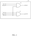
- FIG. 4 is a schematic diagram of a selected circuit in the controller 10.
- the controller 10 may include AND gates 41 and 42 to control access to the planes 141 and 142, respectively.
- the AND gate 41 may receive a plane address signal Sap1, a fail bit pass signal Sfbp and a plane disable signal Sdisp1 to generate a plane select signal Ssp1.
- the AND gate 42 may receive a plane address signal Sap2, the fail bit pass signal Sfbp and a plane disable signal Sdisp2 to generate a plane select signal Ssp2.
- the controller 10 may generate the column address signal Scadr1 according to the plane select signal Sspl, generate the column address signal Scadr2 according to the plane select signal Ssp2, and generate the row address signal Sradr according to the plane select signals Sspl, Ssp2.
- the controller 10 may set the plane disable signal Sdisp1 a logical low, the AND gate 41 may block the plane select signal Ssp1 in response to the plane disable signal Sdisp1 by setting the plane select signal Ssp1 to the logical low, and the controller 10 may generate the row address signal Sradr and the column address signal Scadr1 to deselect the word lines WL1(1) to WL1(N) and the bit lines BL1(1) to BL1(M) of the plane 141.
- the controller 10 may set the plane disable signal Sdisp2 to the logical low, the AND gate 42 may block the plane select signal Ssp2 in response to the plane disable signal Sdisp2 by setting the plane select signal Ssp2 to the logical low, and the controller 10 may generate the row address signal Sradr and the column address signal Scadr2 to deselect the word lines WL2(1) to WL2(N) and the bit lines BL2(1) to BL2(M) of the plane 142.
- the AND gate 41 may receive a first block address signal in place of the plane address signal Sap1 to generate a first block select signal
- the AND gate 42 may receive a second block address signal in place of the plane address signal Sap2 to generate a second block select signal.
- the controller 10 may generate the column address signal Scadr1 according to the first block select signal, generate the column address signal Scadr2 according to the second block select signal, and generate the row address signal Sradr according to the first block select signal and the second block select signal.
- the controller 10 may set the plane disable signal Sdisp1 to the logical low, the AND gate 41 may block the first block select signal in response to the plane disable signal Sdisp1 by setting the first block select signal to the logical low, and the controller 10 may generate the row address signal Sradr and the column address signal Scadr1 to deselect the word lines WL1(1) to WL1(N) and the bit lines BL1(1) to BL1(M) of the plane 141.
- the controller 10 may set the plane disable signal Sdisp2 to the logical low, the AND gate 42 may block the second block select signal in response to the plane disable signal Sdisp2 by setting the second block select signal to the logical low, and the controller 10 may generate the row address signal Sradr and the column address signal Scadr2 to deselect the word lines WL2(1) to WL2(N) and the bit lines BL2(1) to BL2(M) of the plane 142.
- the controller 10 may employ a program state counter q, failed verification counts Cvfl, Cvf2 and a program pulse count Cp to generate the plane disable signals Sdispl, Sdisp2 to control access to the planes 141, 142.
- the program state counter q may be a positive integer ranging between 1 and (Q-1).
- the failed verification counts Cvfl, Cvf2 may be positive integers ranging between 1 and a maximum failure count Cvmax (q).
- the maximum failure count Cvmax(q) may define the maximum number of times to perform verifications of a program state S(q) prior to disabling a plane, and may be specific to the program state S(q).
- the program states S(1) to S(7) may be assigned maximum failure counts Cvmax(1) to Cvmax(7), respectively.
- the maximum failure count Cvmax(q) may be a positive integer greater than 1, and may be set during a manufacturing setup.
- the program pulse count Cp may be positive integers ranging between 1 and a maximum program pulse count Cpmax.
- the maximum program pulse count Cpmax may define the maximum number of times to apply program pulses to the planes 141, 142, and may be a positive integer greater than 1 and set during the manufacturing setup.
- the controller 10 may disable the planes 141, 142 for the subsequent programming, thereby accelerating data programming and reducing program disturbance in the operating plane.
- FIG. 5 is a flowchart of a method 500 of programming the memory device 1.
- the method 500 comprises Steps S502 to S542, performing multi-plane program on the planes 141, 142 and disabling the planes 141, 142 according to respective failed verification counts Cvfl, Cvf2 of the planes 141, 142.
- Steps S502 to S508 are used to program and verify the memory device 1.
- Steps S512 to S516 are used to determine whether to disable the plane 141.
- Steps S522 to S526 are used to determine whether to disable the plane 142.
- Steps S532 to S536 are used to complete programming of the program-enabled planes 141, 142.
- Steps S540 and S542 are used to disable programming of the memory device 1 according to a program pulse count Cp. Any reasonable step change or adjustment is within the scope of the disclosure. Steps S502 to S542 are explained as follows:
- the method 500 may be exemplified using the memory device 1 and TLC memory cells to illustrate details of Steps.
- the planes 141, 142 are initialized for programming.
- the controller 10 sets the plane disable signals Sdispl, Sdisp2 and the fail bit pass signal Sfbp to the logical high, and sets the program pulse count Cp, the failed verification counts Cvfl, Cvf2 to and the program state counter q (S502).
- the controller 10 verifies if memory cells of the planes 141, 142 has reached the program state S(1) (S508). If more than a preset number of the memory cells of the planes 141, 142 have failed to reach the program state S(1), the controller 10 will verify the planes 141, 142 as failed. If less than the preset number of the memory cells of the planes 141, 142 have failed to reach the program state S(1), the controller 10 will verify the planes 141, 142 as passed.
- the controller 10 next determines whether the failed verification count Cvf1 is less than a maximum failure count Cvmax(1) of the program state S(1) (S512).
- Step S540 the controller 10 determines whether the program pulse count Cp is less than the maximum program pulse count Cpmax. In some embodiments, the maximum program pulse count Cpmax may be 20.
- the controller 10 iterates over Steps S504 to S514 and Step S540 until the plane 141 remains verified as failed when the failed verification count Cvf1 reaches 4.
- Step S504 the controller 10 iterates over Steps S504 to S508, Steps S520 to S524 and Step S540 until the plane 142 remains verified as failed when the failed verification count Cvf2 reaches 4.
- the controller 10 sets the plane disable signal Sdisp2 to the logical low while maintaining the fail bit pass signal Sfbp to the logical high to disable the plane 142 (S526).
- the controller 10 next determines whether the program state S(1) is less than the highest program state S(7) (S532).
- the controller 10 iterates over S504 to S514, Steps S530 to S534, and Step S540 until the plane 141 is disabled, the highest program state S(7) is reached, or the program pulse count Cp reaches the maximum program pulse count Cpmax.
- the controller 10 sets the plane disable signal Sdisp1 and the fail bit pass signal Sfbp to the logical low, generates a status report indicating that a program failure and exits the method 500 (S516).
- the controller 10 When the highest program state S(7) is reached, the controller 10 generates the status report indicating that a program pass and exits the method 500 (S536).
- the controller 10 sets the fail bit pass signal Sfbp to the logic low, generates the status report indicating that a program failure and exits the method 500 (S542).
- the maximum failure count Cvmax(q) may be identical to or different from other maximum failure counts Cvmax (1) to Cvmax(q-1), Cvmax(q+1) to Cvmax (Q-1).
- the plane disable signals Sdispl, Sdisp2 are set to the logical low to set the plane select signals Sspl, Ssp2 to the logical low, set the first block select signal or the second block select signal to the logical low, or set other signals controlling the word lines WL1(1) to WL1(N), WL2(1) to WL2(N), the bit lines BL1(1) to BL1(M), BL2 (1) to BL2(M), the string select lines SSL1, SSL2, and the ground select lines GSL1, GSL2 to the logical low.
- the fail bit pass signal Sfbp may be set to the logical high to continue programming of the memory device 1.
- the method 500 is used to identify a failed plane upon verifying the plane as failed for a predetermined number of times, and disable the failed plane while continuing to program the operating plane, thereby accelerating data programming and reducing program disturbance in the operating plane.
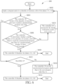
- FIG. 6 is a flowchart of a method 600 of programming the memory device 1.
- the method 600 comprises Steps S602 to S616, disabling the planes 141, 142 according to respective failed verification counts Cvfl, Cvf2 of the plane 141/142.
- Steps S602 and S604 are used to program and verify the memory device 1.
- Steps S606 to S610 are used to determine whether to disable the plane 141/142.
- Steps S612 to S616 are used to continue to complete programming of the program-enabled planes 141, 142. Any reasonable step change or adjustment is within the scope of the disclosure. Steps S602 to S616 are explained as follows:
- Steps S602 to S616 have been provided in the preceding paragraphs and will not be repeated here.
- the controller 10 may disable the failed planes 141, 142 for the subsequent programming, thereby accelerating data programming and reducing program disturbance in the operating plane.
Landscapes
- Engineering & Computer Science (AREA)
- Theoretical Computer Science (AREA)
- Microelectronics & Electronic Packaging (AREA)
- Physics & Mathematics (AREA)
- General Engineering & Computer Science (AREA)
- General Physics & Mathematics (AREA)
- Computer Hardware Design (AREA)
- Human Computer Interaction (AREA)
- Read Only Memory (AREA)
- Techniques For Improving Reliability Of Storages (AREA)
- For Increasing The Reliability Of Semiconductor Memories (AREA)
Claims (11)
- Procédé (500, 600) de programmation d'un dispositif de mémoire (1), le dispositif de mémoire (1) comprenant des plans (141, 142), et un contrôleur (10) couplé aux plans (141, 142), le procédé (500, 600) comprenant les étapes consistant à :appliquer, via le contrôleur (10), une première impulsion de programme à des lignes de mots sélectionnées parmi les plans (141, 142) ;vérifier, via le contrôleur (10), si des cellules de mémoire des plans (141, 142) ont atteint un état de programme prédéterminé (S(Q)) ;en réponse au fait que plus qu'un nombre sélectionné des cellules de mémoire des plans (141, 142) ont échoué à atteindre l'état de programme (S(q)), après que la pluralité de cellules de mémoire ont été vérifiée un nombre prédéterminé de fois, vérifier, via le contrôleur (10), les plans (141, 142) tels qu'ayant échoué ;incrémenter, via le contrôleur (10), un comptage de vérification d'échecs (Cvf1, Cvf2) en réponse au fait que les plans (141, 142) n'ont pas encore été programmés avec succès ;si les plans (141, 142) ont été vérifiés comme ayant échoué le nombre prédéterminé de fois tel que défini par un comptage d'échecs maximum (Cvmax(q)), désactiver, via le contrôleur (10), les plans (141, 142) pour la programmation suivante.
- Procédé (500, 600) selon la revendication 1, comprenant en outre :
en réponse au fait qu'un deuxième plan (142) parmi les plans (141, 142) a été vérifié avec succès, appliquer, via le contrôleur (10), la deuxième impulsion de programme au deuxième plan (142). - Procédé (500, 600) selon la revendication 1, dans lequel l'étape consistant à désactiver, via le contrôleur (10), un premier plan (141) parmi les plans (141, 142) comprend de :
bloquer, via le contrôleur (10), un signal de sélection de plan (Ssp1, Ssp2). - Procédé (500, 600) selon la revendication 1, dans lequel l'étape consistant à désactiver, via le contrôleur (10), un premier plan (141) parmi les plans (141, 142) comprend de :
bloquer, via le contrôleur (10), un signal de sélection de blocage. - Procédé (500, 600) selon la revendication 1, dans lequel l'étape consistant à désactiver, via le contrôleur (10), un premier plan (141) parmi les plans (141, 142) comprend de :
désélectionner, via le contrôleur (10), la totalité des lignes de mots (WL1 (1) à WL1(N)) du premier plan (141). - Procédé (500, 600) selon la revendication 1, dans lequel l'étape consistant à désactiver, via le contrôleur (10), un premier plan (141) parmi les plans (141, 142) comprend de :
désélectionner, via le contrôleur (10), la totalité des lignes de bits (BL1 (1) à BL1(M)) du premier plan (141). - Procédé (500, 600) selon la revendication 1, dans lequel l'étape consistant à désactiver, via le contrôleur (10), un premier plan (141) parmi les plans (141, 142) comprend de :
fixer, via le contrôleur (10), un signal de passage de comptage de bits d'échecs (Sfbp). - Procédé (500, 600) selon la revendication 1, comprenant en outre l'étape consistant à :
fixer, via le contrôleur (10), l'état de programme prédéterminé (S(Q)) à un état de programme suivant (S(Q)) en réponse au fait qu'un des plans (141, 142) a réussi une vérification de l'état de programme prédéterminé (S(Q) et que l'état de programme prédéterminé (S(Q)) n'est pas un état de programme le plus élevé (S(Q)). - Dispositif de mémoire (1), comprenant :des plans (141, 142) ;un contrôleur (10) couplé aux plans (141, 142) et configuré pour :appliquer une première impulsion de programme à des lignes de mots sélectionnées parmi les plans (141, 142);vérifier si des cellules de mémoire des plans of (141, 142) ont atteint un état de programme prédéterminé (S(Q)) ;incrémenter un comptage de vérification d'échecs (Cvf1, Cvf2) en réponse au fait que les plans (141,142) n'ont pas encore été programmés avec succès,vérifier les plans (141, 142) tels qu'ayant échoué, en réponse au fait que plus qu'un nombre sélectionné de cellules de mémoire des plans (141, 142) ont échoué à atteindre l'état de programme (S(q)), après que la pluralité de cellules de mémoire ont été vérifiées un nombre prédéterminé de fois ;si les plans (141, 142) sont vérifiés tels qu'ayant échoué le nombre prédéterminé de fois tel que défini par un comptage d'échecs maximum (Cvmax(q)), le contrôleur (10) désactive les plans (141, 142) pour la programmation suivante.
- Dispositif de mémoire (1) selon la revendication 9, dans lequel le contrôleur est configuré pour : en réponse au fait qu'un deuxième plan (142) parmi les plans (141, 142) a été vérifié avec succès, appliquer la deuxième impulsion de programme au deuxième plan (142).
- Dispositif de mémoire (1) selon la revendication 9, dans lequel le fait de désactiver un premier plan (141) parmi les plans (141, 142) comprend de : bloquer un signal de sélection de plan (Ssp1, Ssp2).
Priority Applications (1)
| Application Number | Priority Date | Filing Date | Title |
|---|---|---|---|
| EP24152294.5A EP4332973B1 (fr) | 2020-02-20 | 2020-02-20 | Procédé de programmation d'un dispositif de mémoire multi-plan |
Applications Claiming Priority (3)
| Application Number | Priority Date | Filing Date | Title |
|---|---|---|---|
| EP24152294.5A EP4332973B1 (fr) | 2020-02-20 | 2020-02-20 | Procédé de programmation d'un dispositif de mémoire multi-plan |
| EP20913055.8A EP3899711B1 (fr) | 2020-02-20 | 2020-02-20 | Procédé de programmation d'un dispositif de mémoire à plans multiples |
| PCT/CN2020/075936 WO2021163945A1 (fr) | 2020-02-20 | 2020-02-20 | Procédé de programmation d'un dispositif de mémoire à plans multiples |
Related Parent Applications (1)
| Application Number | Title | Priority Date | Filing Date |
|---|---|---|---|
| EP20913055.8A Division EP3899711B1 (fr) | 2020-02-20 | 2020-02-20 | Procédé de programmation d'un dispositif de mémoire à plans multiples |
Publications (3)
| Publication Number | Publication Date |
|---|---|
| EP4332973A2 EP4332973A2 (fr) | 2024-03-06 |
| EP4332973A3 EP4332973A3 (fr) | 2024-05-01 |
| EP4332973B1 true EP4332973B1 (fr) | 2025-05-14 |
Family
ID=71197892
Family Applications (2)
| Application Number | Title | Priority Date | Filing Date |
|---|---|---|---|
| EP24152294.5A Active EP4332973B1 (fr) | 2020-02-20 | 2020-02-20 | Procédé de programmation d'un dispositif de mémoire multi-plan |
| EP20913055.8A Active EP3899711B1 (fr) | 2020-02-20 | 2020-02-20 | Procédé de programmation d'un dispositif de mémoire à plans multiples |
Family Applications After (1)
| Application Number | Title | Priority Date | Filing Date |
|---|---|---|---|
| EP20913055.8A Active EP3899711B1 (fr) | 2020-02-20 | 2020-02-20 | Procédé de programmation d'un dispositif de mémoire à plans multiples |
Country Status (7)
| Country | Link |
|---|---|
| US (4) | US11133077B2 (fr) |
| EP (2) | EP4332973B1 (fr) |
| JP (1) | JP7186892B2 (fr) |
| KR (2) | KR20240135689A (fr) |
| CN (2) | CN112965667B (fr) |
| TW (1) | TWI747219B (fr) |
| WO (1) | WO2021163945A1 (fr) |
Families Citing this family (12)
| Publication number | Priority date | Publication date | Assignee | Title |
|---|---|---|---|---|
| EP4332973B1 (fr) | 2020-02-20 | 2025-05-14 | Yangtze Memory Technologies Co., Ltd. | Procédé de programmation d'un dispositif de mémoire multi-plan |
| KR20250020715A (ko) | 2020-04-23 | 2025-02-11 | 양쯔 메모리 테크놀로지스 씨오., 엘티디. | 메모리 디바이스 및 그것의 프로그래밍 방법 |
| US11657883B2 (en) | 2021-07-22 | 2023-05-23 | Western Digital Technologies, Inc. | Isolating problematic memory planes to avoid neighbor plan disturb |
| CN113994315A (zh) | 2021-08-30 | 2022-01-28 | 长江存储科技有限责任公司 | 存储器及其操作方法、存储器系统 |
| WO2023028898A1 (fr) * | 2021-08-31 | 2023-03-09 | 长江存储科技有限责任公司 | Procédé de programmation pour appareil de stockage, appareil de stockage et système de stockage |
| CN113539336B (zh) * | 2021-09-14 | 2021-12-14 | 浙江地芯引力科技有限公司 | 存储器电路系统、设备及写入方法 |
| US11967383B2 (en) | 2022-01-20 | 2024-04-23 | Western Digital Technologies, Inc. | Non-volatile memory with enhanced program operation for last state on slow plane |
| US11862256B2 (en) * | 2022-02-22 | 2024-01-02 | Sandisk Technologies Llc | Non-volatile memory with plane independent screening |
| CN115376597A (zh) * | 2022-07-18 | 2022-11-22 | 长江存储科技有限责任公司 | 存储器的编程方法、存储器及存储系统 |
| CN118262770A (zh) * | 2022-12-26 | 2024-06-28 | 长江存储科技有限责任公司 | 数字验证失败位计数(vfc)电路 |
| US12608136B2 (en) * | 2023-01-10 | 2026-04-21 | Silicon Motion, Inc. | Flash memory scheme capable of controlling flash memory device automatically generating debug information and transmitting debug information back to flash memory controller with making memory cell array generating errors |
| CN119229933B (zh) * | 2023-06-30 | 2026-01-27 | 长江存储科技有限责任公司 | 存储器的操作方法、存储器及存储器系统 |
Family Cites Families (43)
| Publication number | Priority date | Publication date | Assignee | Title |
|---|---|---|---|---|
| JPH1055688A (ja) * | 1996-08-12 | 1998-02-24 | Sony Corp | 不揮発性半導体記憶装置 |
| KR100335769B1 (ko) * | 1999-12-29 | 2002-05-09 | 박종섭 | 플래쉬 메모리 소자의 프로그램 방법 |
| US6504742B1 (en) * | 2001-10-31 | 2003-01-07 | Hewlett-Packard Company | 3-D memory device for large storage capacity |
| US6920523B2 (en) * | 2002-10-07 | 2005-07-19 | Infineon Technologies Ag | Bank address mapping according to bank retention time in dynamic random access memories |
| US7139864B2 (en) * | 2003-12-30 | 2006-11-21 | Sandisk Corporation | Non-volatile memory and method with block management system |
| KR100590388B1 (ko) * | 2005-03-10 | 2006-06-19 | 주식회사 하이닉스반도체 | 멀티-플레인 타입 플래쉬 메모리 장치와, 그 프로그램 동작및 리드 동작 제어 방법 |
| JP4796126B2 (ja) * | 2005-03-31 | 2011-10-19 | サンディスク コーポレイション | メモリセルの部分集合を個別に検証してさらにソフトプログラミングすることによる不揮発性メモリのソフトプログラミング |
| JP5112086B2 (ja) * | 2007-01-17 | 2013-01-09 | 株式会社東芝 | 半導体記憶装置 |
| US7768836B2 (en) * | 2008-10-10 | 2010-08-03 | Sandisk Corporation | Nonvolatile memory and method with reduced program verify by ignoring fastest and/or slowest programming bits |
| US8400854B2 (en) * | 2009-09-11 | 2013-03-19 | Sandisk Technologies Inc. | Identifying at-risk data in non-volatile storage |
| US8174895B2 (en) * | 2009-12-15 | 2012-05-08 | Sandisk Technologies Inc. | Programming non-volatile storage with fast bit detection and verify skip |
| KR101088450B1 (ko) * | 2009-12-31 | 2011-12-01 | 주식회사 하이닉스반도체 | 반도체 메모리 장치 |
| US8248850B2 (en) * | 2010-01-28 | 2012-08-21 | Sandisk Technologies Inc. | Data recovery for non-volatile memory based on count of data state-specific fails |
| US9122476B2 (en) * | 2010-12-07 | 2015-09-01 | Advanced Micro Devices, Inc. | Programmable atomic memory using hardware validation agent |
| US9003102B2 (en) * | 2011-08-26 | 2015-04-07 | Sandisk Technologies Inc. | Controller with extended status register and method of use therewith |
| JP5249394B2 (ja) | 2011-09-28 | 2013-07-31 | ウィンボンド エレクトロニクス コーポレーション | 半導体記憶装置 |
| KR101855169B1 (ko) * | 2011-10-13 | 2018-05-09 | 삼성전자주식회사 | 불휘발성 메모리 장치, 불휘발성 메모리 장치의 프로그램 방법, 불휘발성 메모리 장치를 포함하는 메모리 시스템 |
| KR20130072667A (ko) * | 2011-12-22 | 2013-07-02 | 에스케이하이닉스 주식회사 | 반도체 메모리 장치 및 이의 동작방법 |
| US9043661B2 (en) * | 2012-05-30 | 2015-05-26 | Micron Technology, Inc. | Memories and methods for performing column repair |
| KR102137075B1 (ko) * | 2013-09-10 | 2020-07-23 | 에스케이하이닉스 주식회사 | 반도체 메모리 장치 및 그 프로그램 방법 |
| KR102235492B1 (ko) * | 2014-08-25 | 2021-04-05 | 삼성전자주식회사 | 불휘발성 메모리 장치 및 그것의 프로그램 검증 방법 |
| KR20160072706A (ko) * | 2014-12-15 | 2016-06-23 | 에스케이하이닉스 주식회사 | 반도체 장치 및 이의 동작 방법 |
| US9543023B2 (en) * | 2015-01-23 | 2017-01-10 | Sandisk Technologies Llc | Partial block erase for block programming in non-volatile memory |
| US9672920B2 (en) * | 2015-03-13 | 2017-06-06 | Macronix International Co., Ltd. | Electronic device, non-volatile memorty device, and programming method |
| TWI537964B (zh) * | 2015-04-20 | 2016-06-11 | 華邦電子股份有限公司 | 反及閘快閃記憶體和其操作方法 |
| US9570179B2 (en) * | 2015-04-22 | 2017-02-14 | Sandisk Technologies Llc | Non-volatile memory with two phased programming |
| KR102313017B1 (ko) * | 2015-08-21 | 2021-10-18 | 삼성전자주식회사 | 불휘발성 메모리 장치 및 불휘발성 메모리 장치의 쓰기를 제어하는 컨트롤러를 포함하는 스토리지 장치 및 스토리지 장치의 동작 방법 |
| US20170123994A1 (en) * | 2015-10-28 | 2017-05-04 | Sandisk Technologies Inc. | Handling Of Plane Failure In Non-Volatile Storage |
| KR102391514B1 (ko) * | 2015-11-04 | 2022-04-27 | 삼성전자주식회사 | 메모리 장치 및 메모리 장치의 동작 방법 |
| US10026487B2 (en) * | 2016-06-03 | 2018-07-17 | Sandisk Technologies Llc | Non-volatile memory with customized control of injection type of disturb during program verify for improved program performance |
| KR102651425B1 (ko) * | 2016-06-30 | 2024-03-28 | 에스케이하이닉스 주식회사 | 메모리 시스템 및 메모리 시스템의 동작 방법 |
| KR102738076B1 (ko) * | 2016-11-30 | 2024-12-05 | 삼성전자주식회사 | 루프 상태 정보를 생성하는 불휘발성 메모리 장치, 그것을 포함하는 저장 장치 및 그것의 동작 방법 |
| KR102530337B1 (ko) * | 2017-05-31 | 2023-05-08 | 마이크로소프트 테크놀로지 라이센싱, 엘엘씨 | Ipsec 지오그래픽 리던던시에 대한 분리 제어 및 데이터 평면 동기화 |
| US10360947B2 (en) * | 2017-08-31 | 2019-07-23 | Micron Technology, Inc. | NAND cell encoding to improve data integrity |
| CN109509503B (zh) * | 2017-09-14 | 2021-07-16 | 旺宏电子股份有限公司 | 编程非易失性存储器的方法及存储器系统 |
| US10614886B2 (en) * | 2017-09-22 | 2020-04-07 | Samsung Electronics Co., Ltd. | Nonvolatile memory device and a method of programming the nonvolatile memory device |
| US10134474B1 (en) * | 2017-10-20 | 2018-11-20 | Sandisk Technologies Llc | Independent state completion for each plane during flash memory programming |
| KR102524916B1 (ko) * | 2018-03-13 | 2023-04-26 | 에스케이하이닉스 주식회사 | 저장 장치 및 그 동작 방법 |
| CN108549588A (zh) * | 2018-03-27 | 2018-09-18 | 深圳忆联信息系统有限公司 | 一种消除tlc闪存多片编程失败的方法 |
| CN110400594A (zh) * | 2018-04-24 | 2019-11-01 | 中国科学院微电子研究所 | 一种闪存存储器及其编程验证系统和编程验证方法 |
| US10726923B2 (en) * | 2018-11-21 | 2020-07-28 | Sandisk Technologies Llc | Bias scheme for dummy lines of data storage devices |
| CN110619916A (zh) * | 2019-08-12 | 2019-12-27 | 长江存储科技有限责任公司 | 存储器编程方法、装置、电子设备及可读存储介质 |
| EP4332973B1 (fr) * | 2020-02-20 | 2025-05-14 | Yangtze Memory Technologies Co., Ltd. | Procédé de programmation d'un dispositif de mémoire multi-plan |
-
2020
- 2020-02-20 EP EP24152294.5A patent/EP4332973B1/fr active Active
- 2020-02-20 KR KR1020247029804A patent/KR20240135689A/ko active Pending
- 2020-02-20 JP JP2021549843A patent/JP7186892B2/ja active Active
- 2020-02-20 KR KR1020217024066A patent/KR102709099B1/ko active Active
- 2020-02-20 CN CN202110301415.2A patent/CN112965667B/zh active Active
- 2020-02-20 WO PCT/CN2020/075936 patent/WO2021163945A1/fr not_active Ceased
- 2020-02-20 CN CN202080000277.8A patent/CN111356980B/zh active Active
- 2020-02-20 EP EP20913055.8A patent/EP3899711B1/fr active Active
- 2020-03-30 TW TW109110832A patent/TWI747219B/zh active
- 2020-04-23 US US16/857,124 patent/US11133077B2/en active Active
-
2021
- 2021-08-26 US US17/412,255 patent/US11776641B2/en active Active
-
2023
- 2023-07-28 US US18/227,505 patent/US12347501B2/en active Active
-
2025
- 2025-06-03 US US19/227,035 patent/US20250292846A1/en active Pending
Also Published As
| Publication number | Publication date |
|---|---|
| WO2021163945A1 (fr) | 2021-08-26 |
| US11133077B2 (en) | 2021-09-28 |
| EP3899711B1 (fr) | 2024-02-07 |
| US20250292846A1 (en) | 2025-09-18 |
| CN112965667A (zh) | 2021-06-15 |
| CN112965667B (zh) | 2024-08-16 |
| KR20240135689A (ko) | 2024-09-11 |
| JP2022524728A (ja) | 2022-05-10 |
| KR102709099B1 (ko) | 2024-09-23 |
| CN111356980B (zh) | 2021-03-12 |
| EP4332973A2 (fr) | 2024-03-06 |
| US20230368853A1 (en) | 2023-11-16 |
| TWI747219B (zh) | 2021-11-21 |
| EP4332973A3 (fr) | 2024-05-01 |
| US12347501B2 (en) | 2025-07-01 |
| EP3899711A1 (fr) | 2021-10-27 |
| US20210383882A1 (en) | 2021-12-09 |
| JP7186892B2 (ja) | 2022-12-09 |
| EP3899711A4 (fr) | 2022-07-27 |
| KR20210109593A (ko) | 2021-09-06 |
| TW202133168A (zh) | 2021-09-01 |
| US11776641B2 (en) | 2023-10-03 |
| CN111356980A (zh) | 2020-06-30 |
| US20210264994A1 (en) | 2021-08-26 |
Similar Documents
| Publication | Publication Date | Title |
|---|---|---|
| EP4332973B1 (fr) | Procédé de programmation d'un dispositif de mémoire multi-plan | |
| US7558114B2 (en) | Flash memory device capable of improving reliability | |
| EP1894206B1 (fr) | Effacement de blocs memoire dans un dispositif de memoire flash | |
| US20050141283A1 (en) | Non-volatile semiconductor memory device using differential start programming voltage and programming method thereof | |
| JP7732014B2 (ja) | メモリデバイスおよびそのプログラミング方法 | |
| TWI740780B (zh) | 半導體儲存裝置以及讀出方法 | |
| KR102702652B1 (ko) | 메모리 장치 | |
| US20250342890A1 (en) | Methods for programming a memory device, memory devices, and memory systems | |
| US7450417B2 (en) | Nonvolatile semiconductor memory device |
Legal Events
| Date | Code | Title | Description |
|---|---|---|---|
| PUAI | Public reference made under article 153(3) epc to a published international application that has entered the european phase |
Free format text: ORIGINAL CODE: 0009012 |
|
| STAA | Information on the status of an ep patent application or granted ep patent |
Free format text: STATUS: REQUEST FOR EXAMINATION WAS MADE |
|
| 17P | Request for examination filed |
Effective date: 20240117 |
|
| AC | Divisional application: reference to earlier application |
Ref document number: 3899711 Country of ref document: EP Kind code of ref document: P |
|
| AK | Designated contracting states |
Kind code of ref document: A2 Designated state(s): AL AT BE BG CH CY CZ DE DK EE ES FI FR GB GR HR HU IE IS IT LI LT LU LV MC MK MT NL NO PL PT RO RS SE SI SK SM TR |
|
| REG | Reference to a national code |
Ref country code: DE Ref legal event code: R079 Free format text: PREVIOUS MAIN CLASS: G11C0029040000 Ref country code: DE Ref legal event code: R079 Ref document number: 602020051478 Country of ref document: DE Free format text: PREVIOUS MAIN CLASS: G11C0029040000 Ipc: G11C0016340000 |
|
| PUAL | Search report despatched |
Free format text: ORIGINAL CODE: 0009013 |
|
| AK | Designated contracting states |
Kind code of ref document: A3 Designated state(s): AL AT BE BG CH CY CZ DE DK EE ES FI FR GB GR HR HU IE IS IT LI LT LU LV MC MK MT NL NO PL PT RO RS SE SI SK SM TR |
|
| RIC1 | Information provided on ipc code assigned before grant |
Ipc: G11C 29/04 20060101ALI20240327BHEP Ipc: G11C 29/00 20060101ALI20240327BHEP Ipc: G11C 29/50 20060101ALI20240327BHEP Ipc: G11C 16/24 20060101ALI20240327BHEP Ipc: G11C 16/10 20060101ALI20240327BHEP Ipc: G11C 16/08 20060101ALI20240327BHEP Ipc: G11C 16/04 20060101ALI20240327BHEP Ipc: G11C 11/56 20060101ALI20240327BHEP Ipc: G11C 8/12 20060101ALI20240327BHEP Ipc: G11C 7/10 20060101ALI20240327BHEP Ipc: G11C 5/02 20060101ALI20240327BHEP Ipc: G11C 16/34 20060101AFI20240327BHEP |
|
| STAA | Information on the status of an ep patent application or granted ep patent |
Free format text: STATUS: EXAMINATION IS IN PROGRESS |
|
| 17Q | First examination report despatched |
Effective date: 20240904 |
|
| GRAP | Despatch of communication of intention to grant a patent |
Free format text: ORIGINAL CODE: EPIDOSNIGR1 |
|
| STAA | Information on the status of an ep patent application or granted ep patent |
Free format text: STATUS: GRANT OF PATENT IS INTENDED |
|
| INTG | Intention to grant announced |
Effective date: 20250107 |
|
| P01 | Opt-out of the competence of the unified patent court (upc) registered |
Free format text: CASE NUMBER: APP_7543/2025 Effective date: 20250213 |
|
| GRAS | Grant fee paid |
Free format text: ORIGINAL CODE: EPIDOSNIGR3 |
|
| GRAA | (expected) grant |
Free format text: ORIGINAL CODE: 0009210 |
|
| STAA | Information on the status of an ep patent application or granted ep patent |
Free format text: STATUS: THE PATENT HAS BEEN GRANTED |
|
| AC | Divisional application: reference to earlier application |
Ref document number: 3899711 Country of ref document: EP Kind code of ref document: P |
|
| AK | Designated contracting states |
Kind code of ref document: B1 Designated state(s): AL AT BE BG CH CY CZ DE DK EE ES FI FR GB GR HR HU IE IS IT LI LT LU LV MC MK MT NL NO PL PT RO RS SE SI SK SM TR |
|
| REG | Reference to a national code |
Ref country code: GB Ref legal event code: FG4D |
|
| REG | Reference to a national code |
Ref country code: CH Ref legal event code: EP |
|
| REG | Reference to a national code |
Ref country code: IE Ref legal event code: FG4D |
|
| REG | Reference to a national code |
Ref country code: DE Ref legal event code: R096 Ref document number: 602020051478 Country of ref document: DE |
|
| REG | Reference to a national code |
Ref country code: NL Ref legal event code: MP Effective date: 20250514 |
|
| PG25 | Lapsed in a contracting state [announced via postgrant information from national office to epo] |
Ref country code: FI Free format text: LAPSE BECAUSE OF FAILURE TO SUBMIT A TRANSLATION OF THE DESCRIPTION OR TO PAY THE FEE WITHIN THE PRESCRIBED TIME-LIMIT Effective date: 20250514 Ref country code: ES Free format text: LAPSE BECAUSE OF FAILURE TO SUBMIT A TRANSLATION OF THE DESCRIPTION OR TO PAY THE FEE WITHIN THE PRESCRIBED TIME-LIMIT Effective date: 20250514 Ref country code: PT Free format text: LAPSE BECAUSE OF FAILURE TO SUBMIT A TRANSLATION OF THE DESCRIPTION OR TO PAY THE FEE WITHIN THE PRESCRIBED TIME-LIMIT Effective date: 20250915 |
|
| REG | Reference to a national code |
Ref country code: LT Ref legal event code: MG9D |
|
| PG25 | Lapsed in a contracting state [announced via postgrant information from national office to epo] |
Ref country code: NO Free format text: LAPSE BECAUSE OF FAILURE TO SUBMIT A TRANSLATION OF THE DESCRIPTION OR TO PAY THE FEE WITHIN THE PRESCRIBED TIME-LIMIT Effective date: 20250814 Ref country code: GR Free format text: LAPSE BECAUSE OF FAILURE TO SUBMIT A TRANSLATION OF THE DESCRIPTION OR TO PAY THE FEE WITHIN THE PRESCRIBED TIME-LIMIT Effective date: 20250815 |
|
| PG25 | Lapsed in a contracting state [announced via postgrant information from national office to epo] |
Ref country code: NL Free format text: LAPSE BECAUSE OF FAILURE TO SUBMIT A TRANSLATION OF THE DESCRIPTION OR TO PAY THE FEE WITHIN THE PRESCRIBED TIME-LIMIT Effective date: 20250514 Ref country code: PL Free format text: LAPSE BECAUSE OF FAILURE TO SUBMIT A TRANSLATION OF THE DESCRIPTION OR TO PAY THE FEE WITHIN THE PRESCRIBED TIME-LIMIT Effective date: 20250514 |
|
| REG | Reference to a national code |
Ref country code: AT Ref legal event code: MK05 Ref document number: 1795530 Country of ref document: AT Kind code of ref document: T Effective date: 20250514 |
|
| PG25 | Lapsed in a contracting state [announced via postgrant information from national office to epo] |
Ref country code: BG Free format text: LAPSE BECAUSE OF FAILURE TO SUBMIT A TRANSLATION OF THE DESCRIPTION OR TO PAY THE FEE WITHIN THE PRESCRIBED TIME-LIMIT Effective date: 20250514 |
|
| PG25 | Lapsed in a contracting state [announced via postgrant information from national office to epo] |
Ref country code: HR Free format text: LAPSE BECAUSE OF FAILURE TO SUBMIT A TRANSLATION OF THE DESCRIPTION OR TO PAY THE FEE WITHIN THE PRESCRIBED TIME-LIMIT Effective date: 20250514 |
|
| PG25 | Lapsed in a contracting state [announced via postgrant information from national office to epo] |
Ref country code: AT Free format text: LAPSE BECAUSE OF FAILURE TO SUBMIT A TRANSLATION OF THE DESCRIPTION OR TO PAY THE FEE WITHIN THE PRESCRIBED TIME-LIMIT Effective date: 20250514 |
|
| PG25 | Lapsed in a contracting state [announced via postgrant information from national office to epo] |
Ref country code: RS Free format text: LAPSE BECAUSE OF FAILURE TO SUBMIT A TRANSLATION OF THE DESCRIPTION OR TO PAY THE FEE WITHIN THE PRESCRIBED TIME-LIMIT Effective date: 20250814 |
|
| PG25 | Lapsed in a contracting state [announced via postgrant information from national office to epo] |
Ref country code: IS Free format text: LAPSE BECAUSE OF FAILURE TO SUBMIT A TRANSLATION OF THE DESCRIPTION OR TO PAY THE FEE WITHIN THE PRESCRIBED TIME-LIMIT Effective date: 20250914 |
|
| PG25 | Lapsed in a contracting state [announced via postgrant information from national office to epo] |
Ref country code: LV Free format text: LAPSE BECAUSE OF FAILURE TO SUBMIT A TRANSLATION OF THE DESCRIPTION OR TO PAY THE FEE WITHIN THE PRESCRIBED TIME-LIMIT Effective date: 20250514 |
|
| PGFP | Annual fee paid to national office [announced via postgrant information from national office to epo] |
Ref country code: GB Payment date: 20251205 Year of fee payment: 7 |
|
| PG25 | Lapsed in a contracting state [announced via postgrant information from national office to epo] |
Ref country code: DK Free format text: LAPSE BECAUSE OF FAILURE TO SUBMIT A TRANSLATION OF THE DESCRIPTION OR TO PAY THE FEE WITHIN THE PRESCRIBED TIME-LIMIT Effective date: 20250514 Ref country code: SM Free format text: LAPSE BECAUSE OF FAILURE TO SUBMIT A TRANSLATION OF THE DESCRIPTION OR TO PAY THE FEE WITHIN THE PRESCRIBED TIME-LIMIT Effective date: 20250514 |
|
| PGFP | Annual fee paid to national office [announced via postgrant information from national office to epo] |
Ref country code: FR Payment date: 20251208 Year of fee payment: 7 |
|
| PG25 | Lapsed in a contracting state [announced via postgrant information from national office to epo] |
Ref country code: CZ Free format text: LAPSE BECAUSE OF FAILURE TO SUBMIT A TRANSLATION OF THE DESCRIPTION OR TO PAY THE FEE WITHIN THE PRESCRIBED TIME-LIMIT Effective date: 20250514 |
|
| PG25 | Lapsed in a contracting state [announced via postgrant information from national office to epo] |
Ref country code: EE Free format text: LAPSE BECAUSE OF FAILURE TO SUBMIT A TRANSLATION OF THE DESCRIPTION OR TO PAY THE FEE WITHIN THE PRESCRIBED TIME-LIMIT Effective date: 20250514 |
|
| PG25 | Lapsed in a contracting state [announced via postgrant information from national office to epo] |
Ref country code: SK Free format text: LAPSE BECAUSE OF FAILURE TO SUBMIT A TRANSLATION OF THE DESCRIPTION OR TO PAY THE FEE WITHIN THE PRESCRIBED TIME-LIMIT Effective date: 20250514 |
|
| PG25 | Lapsed in a contracting state [announced via postgrant information from national office to epo] |
Ref country code: IT Free format text: LAPSE BECAUSE OF FAILURE TO SUBMIT A TRANSLATION OF THE DESCRIPTION OR TO PAY THE FEE WITHIN THE PRESCRIBED TIME-LIMIT Effective date: 20250514 |
|
| REG | Reference to a national code |
Ref country code: DE Ref legal event code: R097 Ref document number: 602020051478 Country of ref document: DE |
|
| PLBE | No opposition filed within time limit |
Free format text: ORIGINAL CODE: 0009261 |
|
| STAA | Information on the status of an ep patent application or granted ep patent |
Free format text: STATUS: NO OPPOSITION FILED WITHIN TIME LIMIT |
|
| REG | Reference to a national code |
Ref country code: CH Ref legal event code: L10 Free format text: ST27 STATUS EVENT CODE: U-0-0-L10-L00 (AS PROVIDED BY THE NATIONAL OFFICE) Effective date: 20260325 |
|
| PGFP | Annual fee paid to national office [announced via postgrant information from national office to epo] |
Ref country code: DE Payment date: 20260217 Year of fee payment: 7 |
|
| 26N | No opposition filed |
Effective date: 20260217 |