EP4336576B1 - Moyen d'éclairage pour un phare de véhicule automobile - Google Patents
Moyen d'éclairage pour un phare de véhicule automobile Download PDFInfo
- Publication number
- EP4336576B1 EP4336576B1 EP22194828.4A EP22194828A EP4336576B1 EP 4336576 B1 EP4336576 B1 EP 4336576B1 EP 22194828 A EP22194828 A EP 22194828A EP 4336576 B1 EP4336576 B1 EP 4336576B1
- Authority
- EP
- European Patent Office
- Prior art keywords
- circuit carrier
- gas outlet
- vias
- micro
- outlet channel
- Prior art date
- Legal status (The legal status is an assumption and is not a legal conclusion. Google has not performed a legal analysis and makes no representation as to the accuracy of the status listed.)
- Active
Links
Images

Classifications
-
- F—MECHANICAL ENGINEERING; LIGHTING; HEATING; WEAPONS; BLASTING
- F21—LIGHTING
- F21S—NON-PORTABLE LIGHTING DEVICES; SYSTEMS THEREOF; VEHICLE LIGHTING DEVICES SPECIALLY ADAPTED FOR VEHICLE EXTERIORS
- F21S41/00—Illuminating devices specially adapted for vehicle exteriors, e.g. headlamps
- F21S41/10—Illuminating devices specially adapted for vehicle exteriors, e.g. headlamps characterised by the light source
- F21S41/19—Attachment of light sources or lamp holders
- F21S41/192—Details of lamp holders, terminals or connectors
-
- F—MECHANICAL ENGINEERING; LIGHTING; HEATING; WEAPONS; BLASTING
- F21—LIGHTING
- F21S—NON-PORTABLE LIGHTING DEVICES; SYSTEMS THEREOF; VEHICLE LIGHTING DEVICES SPECIALLY ADAPTED FOR VEHICLE EXTERIORS
- F21S45/00—Arrangements within vehicle lighting devices specially adapted for vehicle exteriors, for purposes other than emission or distribution of light
- F21S45/20—Promoting gas flow in lighting devices, e.g. directing flow toward the cover glass for demisting
-
- H—ELECTRICITY
- H10—SEMICONDUCTOR DEVICES; ELECTRIC SOLID-STATE DEVICES NOT OTHERWISE PROVIDED FOR
- H10H—INORGANIC LIGHT-EMITTING SEMICONDUCTOR DEVICES HAVING POTENTIAL BARRIERS
- H10H20/00—Individual inorganic light-emitting semiconductor devices having potential barriers, e.g. light-emitting diodes [LED]
- H10H20/80—Constructional details
- H10H20/85—Packages
- H10H20/858—Means for heat extraction or cooling
- H10H20/8582—Means for heat extraction or cooling characterised by their shape
-
- F—MECHANICAL ENGINEERING; LIGHTING; HEATING; WEAPONS; BLASTING
- F21—LIGHTING
- F21S—NON-PORTABLE LIGHTING DEVICES; SYSTEMS THEREOF; VEHICLE LIGHTING DEVICES SPECIALLY ADAPTED FOR VEHICLE EXTERIORS
- F21S41/00—Illuminating devices specially adapted for vehicle exteriors, e.g. headlamps
- F21S41/10—Illuminating devices specially adapted for vehicle exteriors, e.g. headlamps characterised by the light source
-
- B—PERFORMING OPERATIONS; TRANSPORTING
- B60—VEHICLES IN GENERAL
- B60Q—ARRANGEMENT OF SIGNALLING OR LIGHTING DEVICES, THE MOUNTING OR SUPPORTING THEREOF OR CIRCUITS THEREFOR, FOR VEHICLES IN GENERAL
- B60Q1/00—Arrangement of optical signalling or lighting devices, the mounting or supporting thereof or circuits therefor
- B60Q1/0088—Details of electrical connections
-
- F—MECHANICAL ENGINEERING; LIGHTING; HEATING; WEAPONS; BLASTING
- F21—LIGHTING
- F21S—NON-PORTABLE LIGHTING DEVICES; SYSTEMS THEREOF; VEHICLE LIGHTING DEVICES SPECIALLY ADAPTED FOR VEHICLE EXTERIORS
- F21S41/00—Illuminating devices specially adapted for vehicle exteriors, e.g. headlamps
- F21S41/10—Illuminating devices specially adapted for vehicle exteriors, e.g. headlamps characterised by the light source
- F21S41/19—Attachment of light sources or lamp holders
-
- F—MECHANICAL ENGINEERING; LIGHTING; HEATING; WEAPONS; BLASTING
- F21—LIGHTING
- F21S—NON-PORTABLE LIGHTING DEVICES; SYSTEMS THEREOF; VEHICLE LIGHTING DEVICES SPECIALLY ADAPTED FOR VEHICLE EXTERIORS
- F21S45/00—Arrangements within vehicle lighting devices specially adapted for vehicle exteriors, for purposes other than emission or distribution of light
- F21S45/40—Cooling of lighting devices
-
- F—MECHANICAL ENGINEERING; LIGHTING; HEATING; WEAPONS; BLASTING
- F21—LIGHTING
- F21S—NON-PORTABLE LIGHTING DEVICES; SYSTEMS THEREOF; VEHICLE LIGHTING DEVICES SPECIALLY ADAPTED FOR VEHICLE EXTERIORS
- F21S45/00—Arrangements within vehicle lighting devices specially adapted for vehicle exteriors, for purposes other than emission or distribution of light
- F21S45/40—Cooling of lighting devices
- F21S45/47—Passive cooling, e.g. using fins, thermal conductive elements or openings
-
- F—MECHANICAL ENGINEERING; LIGHTING; HEATING; WEAPONS; BLASTING
- F21—LIGHTING
- F21S—NON-PORTABLE LIGHTING DEVICES; SYSTEMS THEREOF; VEHICLE LIGHTING DEVICES SPECIALLY ADAPTED FOR VEHICLE EXTERIORS
- F21S45/00—Arrangements within vehicle lighting devices specially adapted for vehicle exteriors, for purposes other than emission or distribution of light
- F21S45/40—Cooling of lighting devices
- F21S45/47—Passive cooling, e.g. using fins, thermal conductive elements or openings
- F21S45/48—Passive cooling, e.g. using fins, thermal conductive elements or openings with means for conducting heat from the inside to the outside of the lighting devices, e.g. with fins on the outer surface of the lighting device
-
- F—MECHANICAL ENGINEERING; LIGHTING; HEATING; WEAPONS; BLASTING
- F21—LIGHTING
- F21V—FUNCTIONAL FEATURES OR DETAILS OF LIGHTING DEVICES OR SYSTEMS THEREOF; STRUCTURAL COMBINATIONS OF LIGHTING DEVICES WITH OTHER ARTICLES, NOT OTHERWISE PROVIDED FOR
- F21V19/00—Fastening of light sources or lamp holders
- F21V19/001—Fastening of light sources or lamp holders the light sources being semiconductors devices, e.g. LEDs
-
- F—MECHANICAL ENGINEERING; LIGHTING; HEATING; WEAPONS; BLASTING
- F21—LIGHTING
- F21V—FUNCTIONAL FEATURES OR DETAILS OF LIGHTING DEVICES OR SYSTEMS THEREOF; STRUCTURAL COMBINATIONS OF LIGHTING DEVICES WITH OTHER ARTICLES, NOT OTHERWISE PROVIDED FOR
- F21V23/00—Arrangement of electric circuit elements in or on lighting devices
- F21V23/003—Arrangement of electric circuit elements in or on lighting devices the elements being electronics drivers or controllers for operating the light source, e.g. for a LED array
-
- F—MECHANICAL ENGINEERING; LIGHTING; HEATING; WEAPONS; BLASTING
- F21—LIGHTING
- F21V—FUNCTIONAL FEATURES OR DETAILS OF LIGHTING DEVICES OR SYSTEMS THEREOF; STRUCTURAL COMBINATIONS OF LIGHTING DEVICES WITH OTHER ARTICLES, NOT OTHERWISE PROVIDED FOR
- F21V23/00—Arrangement of electric circuit elements in or on lighting devices
- F21V23/003—Arrangement of electric circuit elements in or on lighting devices the elements being electronics drivers or controllers for operating the light source, e.g. for a LED array
- F21V23/004—Arrangement of electric circuit elements in or on lighting devices the elements being electronics drivers or controllers for operating the light source, e.g. for a LED array arranged on a substrate, e.g. a printed circuit board
-
- H—ELECTRICITY
- H05—ELECTRIC TECHNIQUES NOT OTHERWISE PROVIDED FOR
- H05K—PRINTED CIRCUITS; CASINGS OR CONSTRUCTIONAL DETAILS OF ELECTRIC APPARATUS; MANUFACTURE OF ASSEMBLAGES OF ELECTRICAL COMPONENTS
- H05K1/00—Printed circuits
- H05K1/02—Details
- H05K1/0201—Thermal arrangements, e.g. for cooling, heating or preventing overheating
- H05K1/0203—Cooling of mounted components
- H05K1/0204—Cooling of mounted components using means for thermal conduction connection in the thickness direction of the substrate
- H05K1/0206—Cooling of mounted components using means for thermal conduction connection in the thickness direction of the substrate by printed thermal vias
-
- H—ELECTRICITY
- H05—ELECTRIC TECHNIQUES NOT OTHERWISE PROVIDED FOR
- H05K—PRINTED CIRCUITS; CASINGS OR CONSTRUCTIONAL DETAILS OF ELECTRIC APPARATUS; MANUFACTURE OF ASSEMBLAGES OF ELECTRICAL COMPONENTS
- H05K1/00—Printed circuits
- H05K1/02—Details
- H05K1/11—Printed elements for providing electric connections to or between printed circuits
- H05K1/111—Pads for surface mounting, e.g. lay-out
-
- H—ELECTRICITY
- H05—ELECTRIC TECHNIQUES NOT OTHERWISE PROVIDED FOR
- H05K—PRINTED CIRCUITS; CASINGS OR CONSTRUCTIONAL DETAILS OF ELECTRIC APPARATUS; MANUFACTURE OF ASSEMBLAGES OF ELECTRICAL COMPONENTS
- H05K3/00—Apparatus or processes for manufacturing printed circuits
- H05K3/30—Assembling printed circuits with electric components, e.g. with resistors
- H05K3/32—Assembling printed circuits with electric components, e.g. with resistors electrically connecting electric components or wires to printed circuits
- H05K3/34—Assembling printed circuits with electric components, e.g. with resistors electrically connecting electric components or wires to printed circuits by soldering
-
- F—MECHANICAL ENGINEERING; LIGHTING; HEATING; WEAPONS; BLASTING
- F21—LIGHTING
- F21S—NON-PORTABLE LIGHTING DEVICES; SYSTEMS THEREOF; VEHICLE LIGHTING DEVICES SPECIALLY ADAPTED FOR VEHICLE EXTERIORS
- F21S41/00—Illuminating devices specially adapted for vehicle exteriors, e.g. headlamps
- F21S41/10—Illuminating devices specially adapted for vehicle exteriors, e.g. headlamps characterised by the light source
- F21S41/14—Illuminating devices specially adapted for vehicle exteriors, e.g. headlamps characterised by the light source characterised by the type of light source
- F21S41/141—Light emitting diodes [LED]
- F21S41/151—Light emitting diodes [LED] arranged in one or more lines
- F21S41/153—Light emitting diodes [LED] arranged in one or more lines arranged in a matrix
-
- F—MECHANICAL ENGINEERING; LIGHTING; HEATING; WEAPONS; BLASTING
- F21—LIGHTING
- F21W—INDEXING SCHEME ASSOCIATED WITH SUBCLASSES F21K, F21L, F21S and F21V, RELATING TO USES OR APPLICATIONS OF LIGHTING DEVICES OR SYSTEMS
- F21W2102/00—Exterior vehicle lighting devices for illuminating purposes
-
- F—MECHANICAL ENGINEERING; LIGHTING; HEATING; WEAPONS; BLASTING
- F21—LIGHTING
- F21W—INDEXING SCHEME ASSOCIATED WITH SUBCLASSES F21K, F21L, F21S and F21V, RELATING TO USES OR APPLICATIONS OF LIGHTING DEVICES OR SYSTEMS
- F21W2107/00—Use or application of lighting devices on or in particular types of vehicles
- F21W2107/10—Use or application of lighting devices on or in particular types of vehicles for land vehicles
-
- F—MECHANICAL ENGINEERING; LIGHTING; HEATING; WEAPONS; BLASTING
- F21—LIGHTING
- F21Y—INDEXING SCHEME ASSOCIATED WITH SUBCLASSES F21K, F21L, F21S and F21V, RELATING TO THE FORM OR THE KIND OF THE LIGHT SOURCES OR OF THE COLOUR OF THE LIGHT EMITTED
- F21Y2115/00—Light-generating elements of semiconductor light sources
- F21Y2115/10—Light-emitting diodes [LED]
-
- H—ELECTRICITY
- H05—ELECTRIC TECHNIQUES NOT OTHERWISE PROVIDED FOR
- H05K—PRINTED CIRCUITS; CASINGS OR CONSTRUCTIONAL DETAILS OF ELECTRIC APPARATUS; MANUFACTURE OF ASSEMBLAGES OF ELECTRICAL COMPONENTS
- H05K2201/00—Indexing scheme relating to printed circuits covered by H05K1/00
- H05K2201/10—Details of components or other objects attached to or integrated in a printed circuit board
- H05K2201/10007—Types of components
- H05K2201/10106—Light emitting diode [LED]
-
- H—ELECTRICITY
- H05—ELECTRIC TECHNIQUES NOT OTHERWISE PROVIDED FOR
- H05K—PRINTED CIRCUITS; CASINGS OR CONSTRUCTIONAL DETAILS OF ELECTRIC APPARATUS; MANUFACTURE OF ASSEMBLAGES OF ELECTRICAL COMPONENTS
- H05K2203/00—Indexing scheme relating to apparatus or processes for manufacturing printed circuits covered by H05K3/00
- H05K2203/11—Treatments characterised by their effect, e.g. heating, cooling, roughening
- H05K2203/1178—Means for venting or for letting gases escape
-
- H—ELECTRICITY
- H10—SEMICONDUCTOR DEVICES; ELECTRIC SOLID-STATE DEVICES NOT OTHERWISE PROVIDED FOR
- H10H—INORGANIC LIGHT-EMITTING SEMICONDUCTOR DEVICES HAVING POTENTIAL BARRIERS
- H10H20/00—Individual inorganic light-emitting semiconductor devices having potential barriers, e.g. light-emitting diodes [LED]
- H10H20/80—Constructional details
- H10H20/85—Packages
- H10H20/858—Means for heat extraction or cooling
- H10H20/8585—Means for heat extraction or cooling being an interconnection
Definitions
- the invention further relates to a motor vehicle headlight comprising a lighting means.
- Illuminants for motor vehicle headlights are known in the prior art. Such illuminants often comprise an SMD component with a light source, and the SMD component is attached to a circuit carrier.
- the circuit carrier is generally also configured, among other things, to cool the SMD component (or the light source). In the prior art, this is often achieved via so-called microvias, which extend at least partially through the circuit carrier (or from an inner region of the circuit carrier) to the SMD component.
- the SMD component is typically soldered to the circuit carrier. Cavities can form in the solder layer, particularly in soldered joints with large-area solder layers (i.e., a layer that contains solidified solder or solder material (after the soldering process) to create a bonded connection between components).
- the micro-vias are arranged in a two-dimensional hexagonal packing arrangement such that the substantially hexagonal base surfaces of the contact elements are substantially completely penetrated by a plurality of micro-vias, in accordance with the highest area packing density.
- adjacent microvias on the hexagonal base surface of a contact element are arranged substantially directly adjacent to one another, wherein the plurality of microvias preferably have a substantially equal diameter at the contact area.
- the contact area is understood to be the area where the microvias or the contact element contact the solder layer.
- the micro-vias are designed substantially conically or truncated conically along their longitudinal extent, wherein the micro-vias are preferably designed such that a cone diameter or a truncated cone diameter decreases towards the solder layer, wherein in particular an angle between a cone axis or a truncated cone axis and a lateral surface of the cone or the truncated cone is 6° to 15°.
- microvias are arranged in the circuit carrier in such a way that those areas of the assembly section containing the gas outlet channel system are free of microvias.
- only the contact elements are interspersed with microvias.
- the circuit carrier has an outer surface facing the SMD component, on which the assembly section is formed, wherein the circuit carrier has a solder resist layer which is at least partially, preferably completely, around the assembly section on the outer surface.
- the contact elements are coated with a thermally conductive and/or electrically conductive material, in particular with a metal, for example copper, or are formed from a thermally conductive and/or electrically conductive material.
- the circuit carrier may be configured as a multilayer printed circuit board having a metal inlay, preferably a copper inlay, with the microvias being thermally connected to the metal inlay.
- the microvias are filled with metal, in particular copper, and thermally connected to the metal inlay via this metal filling.
- the thermally conductive filling material of the microvias is the same material as the metal inlay of the circuit carrier.
- the hexagonal contact elements form polyhedra, which have a substantially equal hexagonal base area.
- the gas outlet channel system is formed, in particular, between the polyhedra.
- the contact elements can, in particular, have a first number of edge elements and a second number of central elements, wherein the edge elements are arranged at the edge of the component section and wherein the central elements are surrounded by the edge elements.
- at least the central elements, and preferably also the edge elements have a hexagonal base area.
- the base surfaces of the hexagonal contact elements each form a regular hexagon.
- each gas outlet channel section of the gas outlet channel system has a channel width defined as a normal distance between parallel side edges of two adjacent contact elements, wherein the gas outlet channel system is configured such that all gas outlet channel sections have substantially the same channel width.
- the channel width of a gas outlet channel section is preferably 150-250 ⁇ m.
- each gas outlet channel section of the gas outlet channel system has a channel height corresponding to a standard distance between the base area of the circuit carrier and the side of the solder layer facing away from the SMD component.
- the channel height of the gas outlet channel system is constant across the entire assembly section, preferably ranging from 100 to 200 ⁇ m.
- the channel height can, in particular, correspond to the vertical height of the contact elements (preferably the vertical height of the contact elements between the base area and the solder layer). The channel height can thus be understood as the layer thickness of the contact elements.
- connection between the SMD component and the assembly section of the circuit carrier is designed by the solder layer in such a way that the underside of the SMD component, the base area of the circuit carrier and the base areas of the hexagonal contact elements lie in planes which are oriented substantially parallel to one another.
- the plurality of contact elements arranged in a grid at least 50%, preferably more than 75%, preferably more than 85%, particularly preferably more than 95% of the contact elements have a hexagonal base area.
- a motor vehicle headlight can be provided which has a lighting means according to the invention.
- US 2013/087813 A1 discloses a lighting device according to the prior art.
- FIG. 1 shows a schematic sectional view of a lighting device 1 according to the invention for a motor vehicle headlight.
- the lighting device 1 comprises an SMD component 2 with a light source 3 for generating light.
- the SMD component 2 has a top side 2a on which the light source 3 is arranged, whereby the top side 2a is designed to be light-emitting.
- the SMD component 2 further has a bottom side 2b facing away from the light-emitting top side 2a.
- the light source 3 can be a pixel LED light source.
- the lighting device 1 comprises a circuit carrier 4, wherein the SMD component 2 is thermally and electrically connected to the circuit carrier 4 by means of a soldered connection.
- the soldered connection is formed as a solder layer 9, which has soldering material.
- the basic principle for producing such a solder connection is known to a person skilled in the art, which is why it will not be discussed in detail here.
- the solder layer 9 is arranged between the underside 2b of the SMD component 2 and a component mounting section 4a of the circuit carrier 4 and connects the SMD component 2 to the circuit carrier 4.
- the solder connection is produced by a soldering process.
- the soldering process can be a reflow soldering process.
- solder In order to enable a uniform application (or a uniform layer thickness) of solder, it can be advantageous, particularly for large-area solder connections (or component mounting sections 4a), not to apply the solder (during the soldering process) continuously, but to divide the solder into solder segments using a stencil.
- the resulting solder layer 9 (cured after its manufacturing process) is continuous (in particular substantially over the entire assembly section 4a).
- the circuit carrier 4 is in the Figure 1 shown embodiment as a multilayer printed circuit board which has a metal inlay 8, preferably a copper inlay,
- the micro-vias 7 are thermally conductively connected to the metal inlay 8.
- the micro-vias 7 are in particular filled with metal, preferably copper, and connected to the metal inlay 8.
- the assembly section 4a is formed from a plurality of contact elements 5a arranged in a grid and spaced from one another, forming a contact element grid 5.
- Gas outlet channel sections 6a are formed between adjacent contact elements 5a.
- the contact elements 5a are arranged relative to one another in such a way that the gas outlet channel sections 6a form a coherent gas outlet channel system 6 through (or in) the assembly section 4a.
- Each contact element 5a is bordered by a section of the coherent gas outlet channel system 6.
- the gas outlet channel system 6 is designed and configured to allow gases which, during the soldering process, escape from the liquefied solder volume which forms after cooling to form the solder layer 9, via the gas outlet channel system 6 from a volume formed between the underside 2b of the SMD component 2 and the assembly section 4a of the circuit carrier 4.
- the circuit carrier 4 has a plurality of microvias 7 configured for heat conduction, which have a substantially circular cross-section and a longitudinal extension. Heat conduction occurs substantially along the longitudinal extension of the microvias.
- the microvias 7 are arranged in the circuit carrier 4 such that the microvias 7 extend at least partially through the circuit carrier 4 toward the assembly section 4a. extend and penetrate it at least in sections or open at the solder layer 9. As a result, the micro-vias 7 penetrate the assembly section 4a at a contact area of the solder layer 9 for heat dissipation.
- the contact area is formed, in particular, exclusively on the contact elements 5a of the assembly section 4a.
- a number of contact elements 5a have a substantially hexagonal base surface 5b.
- the base surfaces 5b lie in a plane that is oriented substantially parallel to the underside 2b of the SMD component 2.
- the micro-vias 7 are arranged in a two-dimensional hexagonal packing arrangement such that the essentially hexagonal base areas 5b of the contact elements 5a are essentially completely penetrated by a plurality of micro-vias 7, in accordance with the highest area packing density, wherein a minimum distance is preferably present between adjacent micro-vias 7.
- the hexagonal base area 5b of the number of contact elements 5a is thus essentially filled with the micro-vias 7, which have an essentially circular base area.
- Adjacent micro-vias 7 are arranged essentially directly adjacent to one another within the hexagonal base area 5b of the contact elements 5a.
- the plurality of micro-vias 7 can have an essentially equal diameter.
- the microvias 7 have a, in particular maximum, hole inner diameter d at the contact area of the solder layer 9, which is preferably ⁇ 0.5 mm, preferably ⁇ 0.25 mm, particularly preferably ⁇ 0.15 mm.
- the microvias 7 are arranged in the assembly section 4a of the circuit carrier 4 such that those areas of the assembly section 4a that have the gas outlet channel system 6 are free of microvias 7.
- the hexagonal contact elements 5a each have a hexagonal base area 5b of essentially the same size.
- the base areas 5b of the hexagonal contact elements 5a each form a regular hexagon.
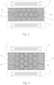
- the contact element surface has five central hexagonal contact elements 5a. These are surrounded by further contact elements, which have other shapes (further polygons) and are also surrounded by micro-vias 7.
- the SMD component 2 is schematically indicated around the assembly section 4a.
- the assembly section 4a has twelve central hexagonal contact elements 5a. These are surrounded by further contact elements, which have different shapes (further polygons) and are also interspersed with microvias 7.
- the SMD component 2 is again schematically indicated around the assembly section 4a.
- the number of hexagonal contact elements 5a is essentially determined by their size and the size and shape of the assembly section 4a.
- Each gas outlet channel section 6a of the gas outlet channel system 6 has a channel width defined as a normal distance between parallel side edges of two adjacent contact elements 5a.
- the gas outlet channel system 6 is preferably configured such that all gas outlet channel sections 6a have the same channel width.
- Each gas outlet channel section 6a of the gas outlet channel system 6 has a channel height corresponding to a normal distance between the base area 4b of the circuit carrier 4 and the side of the solder layer 9 facing away from the SMD component 2.
- the channel height of the gas outlet channel system 6 is constant over the entire assembly section 4a, with the channel height preferably being 100-200 ⁇ m.
- At least 50%, preferably more than 75%, preferably more than 85%, particularly preferably more than 95% have a hexagonal base area 5b.
Landscapes
- Engineering & Computer Science (AREA)
- General Engineering & Computer Science (AREA)
- Microelectronics & Electronic Packaging (AREA)
- Mechanical Engineering (AREA)
- Manufacturing & Machinery (AREA)
- Led Device Packages (AREA)
- Electric Connection Of Electric Components To Printed Circuits (AREA)
- Structures For Mounting Electric Components On Printed Circuit Boards (AREA)
- Fastening Of Light Sources Or Lamp Holders (AREA)
- Production Of Multi-Layered Print Wiring Board (AREA)
- Structure Of Printed Boards (AREA)
Claims (15)
- Moyen d'éclairage (1) pour un phare de véhicule automobile, le moyen d'éclairage (1) comprenant :* un composant CMS (2), comprenant une source lumineuse (3) pour produire de la lumière, le composant CMS (2) présentant une face supérieure émettrice de lumière (2a), sur laquelle est disposée la source lumineuse (3), et une face inférieure (2b) opposée à la face supérieure émettrice de lumière (2a), et* un support de circuit (4), le composant CMS (2) étant relié à une section d'équipement (4a) du support de circuit (4) avec le support de circuit (4) au moyen d'une liaison par brasage de manière à conduire la chaleur et/ou à conduire l'électricité, la liaison par brasage comprenant une couche de brasage (9), qui présente de la soudure, la couche de brasage (9) étant disposée entre la face inférieure (2b) du composant CMS (2) et la section d'équipement (4a) du support de circuit (4) et reliant le composant CMS (2) au support de circuit (4),dans lequella section d'équipement (4a) du support de circuit (4) présente une pluralité d'éléments de contact (5a) disposés selon une trame et espacés les uns des autres, qui s'étendent depuis une surface de base (4b), de préférence plane, du support de circuit (4) en direction du composant CMS (2) et qui sont en contact avec une face de la couche de brasage (9) opposée au composant CMS (2), des sections de canal de sortie de gaz (6a) étant formées entre des éléments de contact (5a) voisins, les éléments de contact (5a) étant disposés les uns par rapport aux autres de telle sorte que les sections de canal de sortie de gaz (6a) forment un système de canaux de sortie de gaz (6) cohérent, de sorte que chaque élément de contact (5a) est bordé par une section du système de canaux de sortie de gaz (6) cohérent, les sections de canal de sortie de gaz (6a) étant délimitées par des surfaces latérales d'éléments de contact (5a) voisins, la surface de base (4b) et le côté de la couche de brasage (9) opposé au composant CMS (2), le système de canaux de sortie de gaz (6) étant conçu et agencé de manière à évacuer les gaz qui s'échappent de la couche de brasage (9) lors du processus de brasage, par le système de canaux de sortie de gaz (6) d'un volume formé entre la couche de brasage (9) et la surface de base (4a) du support de circuit (4),dans lequel, pour l'évacuation de la chaleur dissipée par le composant CMS (2), le support de circuit (4) présente une pluralité de micro-vias (7) aménagées pour la conduction thermique, la conduction thermique s'effectuant essentiellement le long d'une extension longitudinale des micro-vias (7), les micro-vias (7) étant disposés dans le support de circuit (4) de telle sorte, que les micro-vias (7) s'étendent au moins par sections à travers le support de circuit (4) vers la section d'équipement (4a) et traversent la pluralité d'éléments de contact (5a), de sorte que les micro-vias entrent en contact avec la couche de brasage (9) au niveau d'une zone de contact de la couche de brasage (9) pour la dissipation de chaleur, les micro-vias (7) présentant une section transversale sensiblement circulaire au niveau de la zone de contact,dans lequelun certain nombre d'éléments de contact (5a) présentent une surface de base (5b) sensiblement hexagonale, les surfaces de base (5b) étant situées dans un plan qui est orienté sensiblement parallèlement à la surface de base (4b) du support de circuit, et de préférence parallèlement à la face inférieure (2b) du composant CMS (2), les micro-vias (7) étantdisposés les uns par rapport aux autres dans un agencement d'empilement hexagonal bidimensionnel de telle sorte que les surfaces de base (5b) sensiblement hexagonales des éléments de contact (5a) soient traversées par une pluralité de micro-vias (7) sensiblement complètement, selon la densité d'empilement de surface la plus élevée.
- Moyen d'éclairage (1) selon la revendication 1, dans lequel des micro-vias (7) adjacents sont disposés sur la surface de base hexagonale (5b) d'un élément de contact (5a) sensiblement directement adjacents les uns aux autres, de préférence la pluralité de micro-vias (7) sur la zone de contact ayant un diamètre sensiblement égal.
- Moyen d'éclairage (1) selon l'une des revendications précédentes, dans lequel les micro-vias (7) présentent un diamètre intérieur de trou (d) sur la zone de contact, qui est de préférence < 0,5 mm, de préférence < 0,25 mm, de manière particulièrement préférée < 0,15 mm.
- Moyen d'éclairage (1) selon l'une des revendications précédentes, dans lequel les micro-vias (7) ont une forme essentiellement conique ou tronconique le long de leur extension longitudinale, les micro-vias (7) étant de préférence conçus de telle sorte qu'un diamètre de cône ou un diamètre de cône tronqué diminue en direction de la couche de brasage (9), un angle entre un axe de cône ou un axe de cône tronqué et une surface d'enveloppe du cône ou du cône tronqué étant notamment de 6° à 15°.
- Moyen d'éclairage (1) selon l'une des revendications précédentes, dans lequel les micro-vias (7) sont disposés dans le support de circuit (4) de telle sorte que les zones de la section d'équipement (4a) qui présentent le système de canaux de sortie de gaz (6) sont exemptes de micro-vias (7).
- Moyen d'éclairage (1) selon l'une des revendications précédentes, dans lequel le support de circuit (4) présente une surface extérieure tournée vers le composant CMS (2), sur laquelle est formée la section d'équipement (4a), le support de circuit (4) présentant une couche de vernis épargne qui est disposée au moins partiellement, de préférence entièrement, autour de la section d'équipement (4a) sur la surface extérieure.
- Moyen d'éclairage (1) selon l'une des revendications précédentes, dans lequel les éléments de contact (5a) sont revêtus d'un matériau conducteur de la chaleur et/ou de l'électricité, notamment d'un métal, par exemple du cuivre, ou sont formés d'un matériau conducteur de la chaleur et/ou de l'électricité.
- Moyen d'éclairage (1) selon l'une des revendications précédentes, dans lequel le support de circuit (4) est conçu comme une carte de circuit imprimé multicouche, qui présente un inlay métallique (8), de préférence un inlay en cuivre, les micro-vias (7) étant reliés à l'inlay métallique (8) de manière à conduire la chaleur.
- Moyen d'éclairage (1) selon l'une des revendications précédentes, dans lequel les éléments de contact hexagonaux (5a) forment des polyèdres qui présentent une surface de base hexagonale (5b) de taille sensiblement égale.
- Moyen d'éclairage (1) selon l'une des revendications précédentes, dans lequel les surfaces de base (5b) des éléments de contact hexagonaux (5a) forment chacune un hexagone régulier.
- Moyen d'éclairage (1) selon l'une des revendications précédentes, dans lequel chaque section de canal de sortie de gaz (6a) du système de canaux de sortie de gaz (6) présente une largeur de canal qui est définie comme une distance normale entre des bords latéraux parallèles de deux éléments de contact (5a) adjacents, le système de canaux de sortie de gaz (6) étant configuré de telle sorte que toutes les sections de canaux de sortie de gaz (6a) présentent sensiblement la même largeur de canal.
- Moyen d'éclairage (1) selon l'une des revendications précédentes, dans lequel chaque section de canal de sortie de gaz (6a) du système de canaux de sortie de gaz (6) présente une hauteur de canal qui correspond à une distance normale entre la surface de base (4b) du support de circuit (4) et le côté de la couche de brasage (9) opposé au composant CMS (2), la hauteur de canal du système de canaux de sortie de gaz (6) étant de préférence constante sur toute la section d'équipement (4a), la hauteur de canal étant de préférence de 100-200 µm.
- Moyen d'éclairage (1) selon l'une des revendications précédentes, dans lequel la section d'équipement (4a) du support de circuit (4) présente une surface plus grande que la face inférieure (2b) du composant CMS.
- Moyen d'éclairage (1) selon l'une des revendications précédentes, dans lequel, parmi la pluralité d'éléments de contact (5a) disposés selon un quadrillage, au moins 50%, de préférence plus de 75%, de préférence plus de 85%, de manière particulièrement préférée plus de 95% des éléments de contact (5a) présentent une surface de base hexagonale (5b).
- Projecteur de véhicule automobile, comprenant un moyen d'éclairage (1) selon l'une quelconque des revendications précédentes.
Priority Applications (5)
| Application Number | Priority Date | Filing Date | Title |
|---|---|---|---|
| EP22194828.4A EP4336576B1 (fr) | 2022-09-09 | 2022-09-09 | Moyen d'éclairage pour un phare de véhicule automobile |
| KR1020230111758A KR102827078B1 (ko) | 2022-09-09 | 2023-08-25 | 자동차 헤드라이트용 발광 수단 |
| JP2023137010A JP7689550B2 (ja) | 2022-09-09 | 2023-08-25 | 自動車投光機用発光器 |
| US18/241,384 US11982416B2 (en) | 2022-09-09 | 2023-09-01 | Illuminant for vehicle headlamp |
| CN202311150461.2A CN117685525A (zh) | 2022-09-09 | 2023-09-07 | 用于机动车前照灯的发光机构 |
Applications Claiming Priority (1)
| Application Number | Priority Date | Filing Date | Title |
|---|---|---|---|
| EP22194828.4A EP4336576B1 (fr) | 2022-09-09 | 2022-09-09 | Moyen d'éclairage pour un phare de véhicule automobile |
Publications (2)
| Publication Number | Publication Date |
|---|---|
| EP4336576A1 EP4336576A1 (fr) | 2024-03-13 |
| EP4336576B1 true EP4336576B1 (fr) | 2025-04-30 |
Family
ID=83271264
Family Applications (1)
| Application Number | Title | Priority Date | Filing Date |
|---|---|---|---|
| EP22194828.4A Active EP4336576B1 (fr) | 2022-09-09 | 2022-09-09 | Moyen d'éclairage pour un phare de véhicule automobile |
Country Status (5)
| Country | Link |
|---|---|
| US (1) | US11982416B2 (fr) |
| EP (1) | EP4336576B1 (fr) |
| JP (1) | JP7689550B2 (fr) |
| KR (1) | KR102827078B1 (fr) |
| CN (1) | CN117685525A (fr) |
Families Citing this family (1)
| Publication number | Priority date | Publication date | Assignee | Title |
|---|---|---|---|---|
| CN118175729B (zh) * | 2024-05-15 | 2024-08-27 | 浙江万正电子科技股份有限公司 | 一种高散热嵌氮化铝pcb基板及其制作方法 |
Family Cites Families (6)
| Publication number | Priority date | Publication date | Assignee | Title |
|---|---|---|---|---|
| US8587019B2 (en) * | 2011-10-11 | 2013-11-19 | Ledengin, Inc. | Grooved plate for improved solder bonding |
| JP6508468B2 (ja) | 2015-07-24 | 2019-05-08 | 東芝ライテック株式会社 | 車両用照明装置、および車両用灯具 |
| KR102475924B1 (ko) | 2017-08-31 | 2022-12-08 | 쑤저우 레킨 세미컨덕터 컴퍼니 리미티드 | 반도체 소자 및 이를 포함하는 헤드 램프 |
| CN109273423A (zh) * | 2018-08-22 | 2019-01-25 | 宁波天炬光电科技有限公司 | 芯片结构、芯片级封装增强结构及方法 |
| JP7526385B2 (ja) * | 2020-10-27 | 2024-08-01 | 東芝ライテック株式会社 | 車両用照明装置、および車両用灯具 |
| US20230170442A1 (en) * | 2021-12-01 | 2023-06-01 | Lumileds Llc | Die Design Featuring Application Driven Luminance Distribution |
-
2022
- 2022-09-09 EP EP22194828.4A patent/EP4336576B1/fr active Active
-
2023
- 2023-08-25 JP JP2023137010A patent/JP7689550B2/ja active Active
- 2023-08-25 KR KR1020230111758A patent/KR102827078B1/ko active Active
- 2023-09-01 US US18/241,384 patent/US11982416B2/en active Active
- 2023-09-07 CN CN202311150461.2A patent/CN117685525A/zh active Pending
Also Published As
| Publication number | Publication date |
|---|---|
| JP2024039617A (ja) | 2024-03-22 |
| US11982416B2 (en) | 2024-05-14 |
| KR102827078B1 (ko) | 2025-06-27 |
| EP4336576A1 (fr) | 2024-03-13 |
| US20240084989A1 (en) | 2024-03-14 |
| KR20240035704A (ko) | 2024-03-18 |
| CN117685525A (zh) | 2024-03-12 |
| JP7689550B2 (ja) | 2025-06-06 |
Similar Documents
| Publication | Publication Date | Title |
|---|---|---|
| EP1061783B1 (fr) | Substrat céramique-métal, notamment substrat multiple | |
| DE102011079708B4 (de) | Trägervorrichtung, elektrische vorrichtung mit einer trägervorrichtung und verfahren zur herstellung dieser | |
| AT516750B1 (de) | Verfahren zur Voidreduktion in Lötstellen | |
| WO2015043969A2 (fr) | Procédé de soudage par diffusion avec formation d'une zone de diffusion comme assemblage soudé et sous-ensemble électronique doté d'un tel assemblage soudé | |
| EP3695691B1 (fr) | Procédé de génération d'une carte de circuit imprimé avec des trous d'interconnexion thermique, ainsi que carte de circuit imprimé | |
| EP3038436B1 (fr) | Fabrication d'un systeme de commutation comprenant des trous metallises | |
| EP4336576B1 (fr) | Moyen d'éclairage pour un phare de véhicule automobile | |
| DE102006001767A1 (de) | Halbleitermodul mit Halbleiterchips und Verfahren zur Herstellung desselben | |
| DE4326104A1 (de) | Elektrische Baugruppe | |
| DE60034948T2 (de) | Wärmedurchgangslöcher in einer Leiterplatte, um Wärme von oberflächenmontierten elektronischen Bauteilen weg durch die Leiterplatte zu leiten | |
| DE3931551C2 (de) | Verfahren zum Herstellen eines Substrates | |
| DE112019007815T5 (de) | Eine integrierte Miniatur-Schweißplattenstruktur und ihr Herstellungsprozess | |
| EP4101269A1 (fr) | Porteuse composante pour agencer des composants électriques sur une carte de circuit imprimé | |
| DE102021109658B3 (de) | Verfahren zur Herstellung eines Halbleiter-Leistungsgeräts und damit hergestelltes Halbleiter-Leistungsgerät sowie ein Werkzeugteil für eine Sinterpresse und Verwendung einer Sinterpresse | |
| DE3323830C2 (de) | Anordnung zum Auflöten einer elektrischen Schaltungsplatte auf einen Grundkörper | |
| AT520105B1 (de) | Leiterplatte | |
| DE102014224732B4 (de) | Leiterplatte für eine Kraftfahrzeugbeleuchtungseinrichtung mit optimierter Entwärmung | |
| WO2021069448A1 (fr) | Procédé de production d'un module semi-conducteur de puissance et module semi-conducteur de puissance | |
| EP0393496A2 (fr) | Substrat pour plaque de circuit électrique, composé de couches de cuivre et de couches de céramique | |
| DE102011090002A1 (de) | Leiterplatte; Leiterplattenanordnung und Verfahren zur Herstellung einer Leiterplattenanordnung | |
| DE102019129586A1 (de) | Verbindungselement zum Verbinden einer Leiterplatte mit einem Kühlkörper und Verfahren zur Herstellung der Verbindung | |
| DE102019125449B4 (de) | Verfahren zum Herstellen einer Anordnung für eine Leiterplatte und Leiterplatte | |
| DE102018101264A1 (de) | Leiterplatten- Kühlkörper- Aufbau und Verfahren hierzu | |
| EP3503694B1 (fr) | Procédé d'établissement d'une liaison thermoconductrice entre un composant de puissance et une couche métallique d'un support de circuit | |
| DE2252830A1 (de) | Halbleiterbaugruppe und verfahren zu ihrer herstellung |
Legal Events
| Date | Code | Title | Description |
|---|---|---|---|
| PUAI | Public reference made under article 153(3) epc to a published international application that has entered the european phase |
Free format text: ORIGINAL CODE: 0009012 |
|
| STAA | Information on the status of an ep patent application or granted ep patent |
Free format text: STATUS: THE APPLICATION HAS BEEN PUBLISHED |
|
| AK | Designated contracting states |
Kind code of ref document: A1 Designated state(s): AL AT BE BG CH CY CZ DE DK EE ES FI FR GB GR HR HU IE IS IT LI LT LU LV MC MK MT NL NO PL PT RO RS SE SI SK SM TR |
|
| STAA | Information on the status of an ep patent application or granted ep patent |
Free format text: STATUS: REQUEST FOR EXAMINATION WAS MADE |
|
| 17P | Request for examination filed |
Effective date: 20240905 |
|
| RBV | Designated contracting states (corrected) |
Designated state(s): AL AT BE BG CH CY CZ DE DK EE ES FI FR GB GR HR HU IE IS IT LI LT LU LV MC MK MT NL NO PL PT RO RS SE SI SK SM TR |
|
| REG | Reference to a national code |
Ref legal event code: R079 Ipc: H10H0020858000 Ref country code: DE Ref legal event code: R079 Ref document number: 502022003741 Country of ref document: DE Free format text: PREVIOUS MAIN CLASS: H01L0033640000 Ipc: H10H0020858000 |
|
| GRAP | Despatch of communication of intention to grant a patent |
Free format text: ORIGINAL CODE: EPIDOSNIGR1 |
|
| STAA | Information on the status of an ep patent application or granted ep patent |
Free format text: STATUS: GRANT OF PATENT IS INTENDED |
|
| RIC1 | Information provided on ipc code assigned before grant |
Ipc: H05K 1/02 20060101ALI20250116BHEP Ipc: H10H 20/858 20250101AFI20250116BHEP |
|
| INTG | Intention to grant announced |
Effective date: 20250211 |
|
| GRAS | Grant fee paid |
Free format text: ORIGINAL CODE: EPIDOSNIGR3 |
|
| GRAA | (expected) grant |
Free format text: ORIGINAL CODE: 0009210 |
|
| STAA | Information on the status of an ep patent application or granted ep patent |
Free format text: STATUS: THE PATENT HAS BEEN GRANTED |
|
| AK | Designated contracting states |
Kind code of ref document: B1 Designated state(s): AL AT BE BG CH CY CZ DE DK EE ES FI FR GB GR HR HU IE IS IT LI LT LU LV MC MK MT NL NO PL PT RO RS SE SI SK SM TR |
|
| REG | Reference to a national code |
Ref country code: CH Ref legal event code: EP Ref country code: GB Ref legal event code: FG4D Free format text: NOT ENGLISH |
|
| REG | Reference to a national code |
Ref country code: IE Ref legal event code: FG4D Free format text: LANGUAGE OF EP DOCUMENT: GERMAN |
|
| REG | Reference to a national code |
Ref country code: DE Ref legal event code: R096 Ref document number: 502022003741 Country of ref document: DE |
|
| P01 | Opt-out of the competence of the unified patent court (upc) registered |
Free format text: CASE NUMBER: APP_26108/2025 Effective date: 20250602 |
|
| REG | Reference to a national code |
Ref country code: NL Ref legal event code: MP Effective date: 20250430 |
|
| PG25 | Lapsed in a contracting state [announced via postgrant information from national office to epo] |
Ref country code: FI Free format text: LAPSE BECAUSE OF FAILURE TO SUBMIT A TRANSLATION OF THE DESCRIPTION OR TO PAY THE FEE WITHIN THE PRESCRIBED TIME-LIMIT Effective date: 20250430 Ref country code: PT Free format text: LAPSE BECAUSE OF FAILURE TO SUBMIT A TRANSLATION OF THE DESCRIPTION OR TO PAY THE FEE WITHIN THE PRESCRIBED TIME-LIMIT Effective date: 20250901 Ref country code: ES Free format text: LAPSE BECAUSE OF FAILURE TO SUBMIT A TRANSLATION OF THE DESCRIPTION OR TO PAY THE FEE WITHIN THE PRESCRIBED TIME-LIMIT Effective date: 20250430 |
|
| PGFP | Annual fee paid to national office [announced via postgrant information from national office to epo] |
Ref country code: DE Payment date: 20250919 Year of fee payment: 4 |
|
| REG | Reference to a national code |
Ref country code: LT Ref legal event code: MG9D |
|
| PG25 | Lapsed in a contracting state [announced via postgrant information from national office to epo] |
Ref country code: GR Free format text: LAPSE BECAUSE OF FAILURE TO SUBMIT A TRANSLATION OF THE DESCRIPTION OR TO PAY THE FEE WITHIN THE PRESCRIBED TIME-LIMIT Effective date: 20250731 Ref country code: NO Free format text: LAPSE BECAUSE OF FAILURE TO SUBMIT A TRANSLATION OF THE DESCRIPTION OR TO PAY THE FEE WITHIN THE PRESCRIBED TIME-LIMIT Effective date: 20250730 |
|
| PG25 | Lapsed in a contracting state [announced via postgrant information from national office to epo] |
Ref country code: NL Free format text: LAPSE BECAUSE OF FAILURE TO SUBMIT A TRANSLATION OF THE DESCRIPTION OR TO PAY THE FEE WITHIN THE PRESCRIBED TIME-LIMIT Effective date: 20250430 Ref country code: PL Free format text: LAPSE BECAUSE OF FAILURE TO SUBMIT A TRANSLATION OF THE DESCRIPTION OR TO PAY THE FEE WITHIN THE PRESCRIBED TIME-LIMIT Effective date: 20250430 |
|
| PG25 | Lapsed in a contracting state [announced via postgrant information from national office to epo] |
Ref country code: BG Free format text: LAPSE BECAUSE OF FAILURE TO SUBMIT A TRANSLATION OF THE DESCRIPTION OR TO PAY THE FEE WITHIN THE PRESCRIBED TIME-LIMIT Effective date: 20250430 |
|
| PG25 | Lapsed in a contracting state [announced via postgrant information from national office to epo] |
Ref country code: HR Free format text: LAPSE BECAUSE OF FAILURE TO SUBMIT A TRANSLATION OF THE DESCRIPTION OR TO PAY THE FEE WITHIN THE PRESCRIBED TIME-LIMIT Effective date: 20250430 |
|
| PGFP | Annual fee paid to national office [announced via postgrant information from national office to epo] |
Ref country code: AT Payment date: 20251020 Year of fee payment: 4 Ref country code: FR Payment date: 20250922 Year of fee payment: 4 |
|
| PG25 | Lapsed in a contracting state [announced via postgrant information from national office to epo] |
Ref country code: RS Free format text: LAPSE BECAUSE OF FAILURE TO SUBMIT A TRANSLATION OF THE DESCRIPTION OR TO PAY THE FEE WITHIN THE PRESCRIBED TIME-LIMIT Effective date: 20250731 |
|
| PG25 | Lapsed in a contracting state [announced via postgrant information from national office to epo] |
Ref country code: IS Free format text: LAPSE BECAUSE OF FAILURE TO SUBMIT A TRANSLATION OF THE DESCRIPTION OR TO PAY THE FEE WITHIN THE PRESCRIBED TIME-LIMIT Effective date: 20250830 |
|
| PG25 | Lapsed in a contracting state [announced via postgrant information from national office to epo] |
Ref country code: LV Free format text: LAPSE BECAUSE OF FAILURE TO SUBMIT A TRANSLATION OF THE DESCRIPTION OR TO PAY THE FEE WITHIN THE PRESCRIBED TIME-LIMIT Effective date: 20250430 |
|
| PG25 | Lapsed in a contracting state [announced via postgrant information from national office to epo] |
Ref country code: DK Free format text: LAPSE BECAUSE OF FAILURE TO SUBMIT A TRANSLATION OF THE DESCRIPTION OR TO PAY THE FEE WITHIN THE PRESCRIBED TIME-LIMIT Effective date: 20250430 Ref country code: SM Free format text: LAPSE BECAUSE OF FAILURE TO SUBMIT A TRANSLATION OF THE DESCRIPTION OR TO PAY THE FEE WITHIN THE PRESCRIBED TIME-LIMIT Effective date: 20250430 |
|
| PG25 | Lapsed in a contracting state [announced via postgrant information from national office to epo] |
Ref country code: CZ Free format text: LAPSE BECAUSE OF FAILURE TO SUBMIT A TRANSLATION OF THE DESCRIPTION OR TO PAY THE FEE WITHIN THE PRESCRIBED TIME-LIMIT Effective date: 20250430 |
|
| PG25 | Lapsed in a contracting state [announced via postgrant information from national office to epo] |
Ref country code: EE Free format text: LAPSE BECAUSE OF FAILURE TO SUBMIT A TRANSLATION OF THE DESCRIPTION OR TO PAY THE FEE WITHIN THE PRESCRIBED TIME-LIMIT Effective date: 20250430 |
|
| PG25 | Lapsed in a contracting state [announced via postgrant information from national office to epo] |
Ref country code: SK Free format text: LAPSE BECAUSE OF FAILURE TO SUBMIT A TRANSLATION OF THE DESCRIPTION OR TO PAY THE FEE WITHIN THE PRESCRIBED TIME-LIMIT Effective date: 20250430 |
|
| PG25 | Lapsed in a contracting state [announced via postgrant information from national office to epo] |
Ref country code: IT Free format text: LAPSE BECAUSE OF FAILURE TO SUBMIT A TRANSLATION OF THE DESCRIPTION OR TO PAY THE FEE WITHIN THE PRESCRIBED TIME-LIMIT Effective date: 20250430 |
|
| REG | Reference to a national code |
Ref country code: DE Ref legal event code: R097 Ref document number: 502022003741 Country of ref document: DE |
|
| PG25 | Lapsed in a contracting state [announced via postgrant information from national office to epo] |
Ref country code: RO Free format text: LAPSE BECAUSE OF FAILURE TO SUBMIT A TRANSLATION OF THE DESCRIPTION OR TO PAY THE FEE WITHIN THE PRESCRIBED TIME-LIMIT Effective date: 20250430 |
|
| PLBE | No opposition filed within time limit |
Free format text: ORIGINAL CODE: 0009261 |
|
| STAA | Information on the status of an ep patent application or granted ep patent |
Free format text: STATUS: NO OPPOSITION FILED WITHIN TIME LIMIT |
|
| REG | Reference to a national code |
Ref country code: CH Ref legal event code: L10 Free format text: ST27 STATUS EVENT CODE: U-0-0-L10-L00 (AS PROVIDED BY THE NATIONAL OFFICE) Effective date: 20260311 |
|
| 26N | No opposition filed |
Effective date: 20260202 |