EP4340047A1 - Procédé de fabrication d'une couche d'absorption de lumière cigs pour cellule solaire par dépôt chimique en phase vapeur - Google Patents
Procédé de fabrication d'une couche d'absorption de lumière cigs pour cellule solaire par dépôt chimique en phase vapeur Download PDFInfo
- Publication number
- EP4340047A1 EP4340047A1 EP22807676.6A EP22807676A EP4340047A1 EP 4340047 A1 EP4340047 A1 EP 4340047A1 EP 22807676 A EP22807676 A EP 22807676A EP 4340047 A1 EP4340047 A1 EP 4340047A1
- Authority
- EP
- European Patent Office
- Prior art keywords
- thin film
- copper
- gallium
- indium
- forming step
- Prior art date
- Legal status (The legal status is an assumption and is not a legal conclusion. Google has not performed a legal analysis and makes no representation as to the accuracy of the status listed.)
- Pending
Links
Images


Classifications
-
- H—ELECTRICITY
- H10—SEMICONDUCTOR DEVICES; ELECTRIC SOLID-STATE DEVICES NOT OTHERWISE PROVIDED FOR
- H10F—INORGANIC SEMICONDUCTOR DEVICES SENSITIVE TO INFRARED RADIATION, LIGHT, ELECTROMAGNETIC RADIATION OF SHORTER WAVELENGTH OR CORPUSCULAR RADIATION
- H10F77/00—Constructional details of devices covered by this subclass
- H10F77/10—Semiconductor bodies
- H10F77/12—Active materials
- H10F77/126—Active materials comprising only Group I-III-VI chalcopyrite materials, e.g. CuInSe2, CuGaSe2 or CuInGaSe2 [CIGS]
-
- H—ELECTRICITY
- H10—SEMICONDUCTOR DEVICES; ELECTRIC SOLID-STATE DEVICES NOT OTHERWISE PROVIDED FOR
- H10P—GENERIC PROCESSES OR APPARATUS FOR THE MANUFACTURE OR TREATMENT OF DEVICES COVERED BY CLASS H10
- H10P14/00—Formation of materials, e.g. in the shape of layers or pillars
- H10P14/20—Formation of materials, e.g. in the shape of layers or pillars of semiconductor materials
- H10P14/34—Deposited materials, e.g. layers
- H10P14/3402—Deposited materials, e.g. layers characterised by the chemical composition
- H10P14/3436—Deposited materials, e.g. layers characterised by the chemical composition being chalcogenide semiconductor materials not being oxides, e.g. ternary compounds
-
- H—ELECTRICITY
- H10—SEMICONDUCTOR DEVICES; ELECTRIC SOLID-STATE DEVICES NOT OTHERWISE PROVIDED FOR
- H10F—INORGANIC SEMICONDUCTOR DEVICES SENSITIVE TO INFRARED RADIATION, LIGHT, ELECTROMAGNETIC RADIATION OF SHORTER WAVELENGTH OR CORPUSCULAR RADIATION
- H10F71/00—Manufacture or treatment of devices covered by this subclass
- H10F71/128—Annealing
-
- C—CHEMISTRY; METALLURGY
- C23—COATING METALLIC MATERIAL; COATING MATERIAL WITH METALLIC MATERIAL; CHEMICAL SURFACE TREATMENT; DIFFUSION TREATMENT OF METALLIC MATERIAL; COATING BY VACUUM EVAPORATION, BY SPUTTERING, BY ION IMPLANTATION OR BY CHEMICAL VAPOUR DEPOSITION, IN GENERAL; INHIBITING CORROSION OF METALLIC MATERIAL OR INCRUSTATION IN GENERAL
- C23C—COATING METALLIC MATERIAL; COATING MATERIAL WITH METALLIC MATERIAL; SURFACE TREATMENT OF METALLIC MATERIAL BY DIFFUSION INTO THE SURFACE, BY CHEMICAL CONVERSION OR SUBSTITUTION; COATING BY VACUUM EVAPORATION, BY SPUTTERING, BY ION IMPLANTATION OR BY CHEMICAL VAPOUR DEPOSITION, IN GENERAL
- C23C16/00—Chemical coating by decomposition of gaseous compounds, without leaving reaction products of surface material in the coating, i.e. chemical vapour deposition [CVD] processes
- C23C16/06—Chemical coating by decomposition of gaseous compounds, without leaving reaction products of surface material in the coating, i.e. chemical vapour deposition [CVD] processes characterised by the deposition of metallic material
- C23C16/18—Chemical coating by decomposition of gaseous compounds, without leaving reaction products of surface material in the coating, i.e. chemical vapour deposition [CVD] processes characterised by the deposition of metallic material from metallo-organic compounds
-
- C—CHEMISTRY; METALLURGY
- C23—COATING METALLIC MATERIAL; COATING MATERIAL WITH METALLIC MATERIAL; CHEMICAL SURFACE TREATMENT; DIFFUSION TREATMENT OF METALLIC MATERIAL; COATING BY VACUUM EVAPORATION, BY SPUTTERING, BY ION IMPLANTATION OR BY CHEMICAL VAPOUR DEPOSITION, IN GENERAL; INHIBITING CORROSION OF METALLIC MATERIAL OR INCRUSTATION IN GENERAL
- C23C—COATING METALLIC MATERIAL; COATING MATERIAL WITH METALLIC MATERIAL; SURFACE TREATMENT OF METALLIC MATERIAL BY DIFFUSION INTO THE SURFACE, BY CHEMICAL CONVERSION OR SUBSTITUTION; COATING BY VACUUM EVAPORATION, BY SPUTTERING, BY ION IMPLANTATION OR BY CHEMICAL VAPOUR DEPOSITION, IN GENERAL
- C23C16/00—Chemical coating by decomposition of gaseous compounds, without leaving reaction products of surface material in the coating, i.e. chemical vapour deposition [CVD] processes
- C23C16/22—Chemical coating by decomposition of gaseous compounds, without leaving reaction products of surface material in the coating, i.e. chemical vapour deposition [CVD] processes characterised by the deposition of inorganic material, other than metallic material
- C23C16/30—Deposition of compounds, mixtures or solid solutions, e.g. borides, carbides, nitrides
-
- C—CHEMISTRY; METALLURGY
- C23—COATING METALLIC MATERIAL; COATING MATERIAL WITH METALLIC MATERIAL; CHEMICAL SURFACE TREATMENT; DIFFUSION TREATMENT OF METALLIC MATERIAL; COATING BY VACUUM EVAPORATION, BY SPUTTERING, BY ION IMPLANTATION OR BY CHEMICAL VAPOUR DEPOSITION, IN GENERAL; INHIBITING CORROSION OF METALLIC MATERIAL OR INCRUSTATION IN GENERAL
- C23C—COATING METALLIC MATERIAL; COATING MATERIAL WITH METALLIC MATERIAL; SURFACE TREATMENT OF METALLIC MATERIAL BY DIFFUSION INTO THE SURFACE, BY CHEMICAL CONVERSION OR SUBSTITUTION; COATING BY VACUUM EVAPORATION, BY SPUTTERING, BY ION IMPLANTATION OR BY CHEMICAL VAPOUR DEPOSITION, IN GENERAL
- C23C16/00—Chemical coating by decomposition of gaseous compounds, without leaving reaction products of surface material in the coating, i.e. chemical vapour deposition [CVD] processes
- C23C16/22—Chemical coating by decomposition of gaseous compounds, without leaving reaction products of surface material in the coating, i.e. chemical vapour deposition [CVD] processes characterised by the deposition of inorganic material, other than metallic material
- C23C16/30—Deposition of compounds, mixtures or solid solutions, e.g. borides, carbides, nitrides
- C23C16/305—Sulfides, selenides, or tellurides
-
- C—CHEMISTRY; METALLURGY
- C23—COATING METALLIC MATERIAL; COATING MATERIAL WITH METALLIC MATERIAL; CHEMICAL SURFACE TREATMENT; DIFFUSION TREATMENT OF METALLIC MATERIAL; COATING BY VACUUM EVAPORATION, BY SPUTTERING, BY ION IMPLANTATION OR BY CHEMICAL VAPOUR DEPOSITION, IN GENERAL; INHIBITING CORROSION OF METALLIC MATERIAL OR INCRUSTATION IN GENERAL
- C23C—COATING METALLIC MATERIAL; COATING MATERIAL WITH METALLIC MATERIAL; SURFACE TREATMENT OF METALLIC MATERIAL BY DIFFUSION INTO THE SURFACE, BY CHEMICAL CONVERSION OR SUBSTITUTION; COATING BY VACUUM EVAPORATION, BY SPUTTERING, BY ION IMPLANTATION OR BY CHEMICAL VAPOUR DEPOSITION, IN GENERAL
- C23C16/00—Chemical coating by decomposition of gaseous compounds, without leaving reaction products of surface material in the coating, i.e. chemical vapour deposition [CVD] processes
- C23C16/56—After-treatment
-
- H—ELECTRICITY
- H10—SEMICONDUCTOR DEVICES; ELECTRIC SOLID-STATE DEVICES NOT OTHERWISE PROVIDED FOR
- H10F—INORGANIC SEMICONDUCTOR DEVICES SENSITIVE TO INFRARED RADIATION, LIGHT, ELECTROMAGNETIC RADIATION OF SHORTER WAVELENGTH OR CORPUSCULAR RADIATION
- H10F10/00—Individual photovoltaic cells, e.g. solar cells
- H10F10/10—Individual photovoltaic cells, e.g. solar cells having potential barriers
- H10F10/16—Photovoltaic cells having only PN heterojunction potential barriers
- H10F10/167—Photovoltaic cells having only PN heterojunction potential barriers comprising Group I-III-VI materials, e.g. CdS/CuInSe2 [CIS] heterojunction photovoltaic cells
-
- H—ELECTRICITY
- H10—SEMICONDUCTOR DEVICES; ELECTRIC SOLID-STATE DEVICES NOT OTHERWISE PROVIDED FOR
- H10F—INORGANIC SEMICONDUCTOR DEVICES SENSITIVE TO INFRARED RADIATION, LIGHT, ELECTROMAGNETIC RADIATION OF SHORTER WAVELENGTH OR CORPUSCULAR RADIATION
- H10F77/00—Constructional details of devices covered by this subclass
- H10F77/10—Semiconductor bodies
- H10F77/12—Active materials
-
- H—ELECTRICITY
- H10—SEMICONDUCTOR DEVICES; ELECTRIC SOLID-STATE DEVICES NOT OTHERWISE PROVIDED FOR
- H10P—GENERIC PROCESSES OR APPARATUS FOR THE MANUFACTURE OR TREATMENT OF DEVICES COVERED BY CLASS H10
- H10P14/00—Formation of materials, e.g. in the shape of layers or pillars
- H10P14/20—Formation of materials, e.g. in the shape of layers or pillars of semiconductor materials
- H10P14/203—Formation of materials, e.g. in the shape of layers or pillars of semiconductor materials using transformation of metal, e.g. oxidation or nitridation
-
- H—ELECTRICITY
- H10—SEMICONDUCTOR DEVICES; ELECTRIC SOLID-STATE DEVICES NOT OTHERWISE PROVIDED FOR
- H10P—GENERIC PROCESSES OR APPARATUS FOR THE MANUFACTURE OR TREATMENT OF DEVICES COVERED BY CLASS H10
- H10P14/00—Formation of materials, e.g. in the shape of layers or pillars
- H10P14/20—Formation of materials, e.g. in the shape of layers or pillars of semiconductor materials
- H10P14/24—Formation of materials, e.g. in the shape of layers or pillars of semiconductor materials using chemical vapour deposition [CVD]
-
- H—ELECTRICITY
- H10—SEMICONDUCTOR DEVICES; ELECTRIC SOLID-STATE DEVICES NOT OTHERWISE PROVIDED FOR
- H10P—GENERIC PROCESSES OR APPARATUS FOR THE MANUFACTURE OR TREATMENT OF DEVICES COVERED BY CLASS H10
- H10P14/00—Formation of materials, e.g. in the shape of layers or pillars
- H10P14/20—Formation of materials, e.g. in the shape of layers or pillars of semiconductor materials
- H10P14/29—Formation of materials, e.g. in the shape of layers or pillars of semiconductor materials characterised by the substrates
- H10P14/2901—Materials
- H10P14/2922—Materials being non-crystalline insulating materials, e.g. glass or polymers
-
- H—ELECTRICITY
- H10—SEMICONDUCTOR DEVICES; ELECTRIC SOLID-STATE DEVICES NOT OTHERWISE PROVIDED FOR
- H10P—GENERIC PROCESSES OR APPARATUS FOR THE MANUFACTURE OR TREATMENT OF DEVICES COVERED BY CLASS H10
- H10P14/00—Formation of materials, e.g. in the shape of layers or pillars
- H10P14/20—Formation of materials, e.g. in the shape of layers or pillars of semiconductor materials
- H10P14/32—Formation of materials, e.g. in the shape of layers or pillars of semiconductor materials characterised by intermediate layers between substrates and deposited layers
- H10P14/3202—Materials thereof
- H10P14/3241—Materials thereof being conductive materials
-
- Y—GENERAL TAGGING OF NEW TECHNOLOGICAL DEVELOPMENTS; GENERAL TAGGING OF CROSS-SECTIONAL TECHNOLOGIES SPANNING OVER SEVERAL SECTIONS OF THE IPC; TECHNICAL SUBJECTS COVERED BY FORMER USPC CROSS-REFERENCE ART COLLECTIONS [XRACs] AND DIGESTS
- Y02—TECHNOLOGIES OR APPLICATIONS FOR MITIGATION OR ADAPTATION AGAINST CLIMATE CHANGE
- Y02E—REDUCTION OF GREENHOUSE GAS [GHG] EMISSIONS, RELATED TO ENERGY GENERATION, TRANSMISSION OR DISTRIBUTION
- Y02E10/00—Energy generation through renewable energy sources
- Y02E10/50—Photovoltaic [PV] energy
- Y02E10/541—CuInSe2 material PV cells
-
- Y—GENERAL TAGGING OF NEW TECHNOLOGICAL DEVELOPMENTS; GENERAL TAGGING OF CROSS-SECTIONAL TECHNOLOGIES SPANNING OVER SEVERAL SECTIONS OF THE IPC; TECHNICAL SUBJECTS COVERED BY FORMER USPC CROSS-REFERENCE ART COLLECTIONS [XRACs] AND DIGESTS
- Y02—TECHNOLOGIES OR APPLICATIONS FOR MITIGATION OR ADAPTATION AGAINST CLIMATE CHANGE
- Y02P—CLIMATE CHANGE MITIGATION TECHNOLOGIES IN THE PRODUCTION OR PROCESSING OF GOODS
- Y02P70/00—Climate change mitigation technologies in the production process for final industrial or consumer products
- Y02P70/50—Manufacturing or production processes characterised by the final manufactured product
Definitions
- the present invention relates to a manufacturing method of a CIGS light absorption layer for solar cell using chemical vapor deposition. More specifically, it relates to a manufacturing method of a CIGS light absorption layer for solar cell using chemical vapor deposition that effectively controls a MoSe x layer and thereby exhibits a high energy conversion efficiency.
- These solar cells are manufactured by using single crystal or polycrystalline silicon wafers, but single crystal silicon generally has the highest photovoltaic efficiency and thus is widely used in large-scale power generation systems and others.
- this single crystal silicon has the disadvantage that the manufacturing process is complicated and the price of cells or modules varies greatly depending on silicon price trend.
- CIGS Cu (In 1-x Ga x )Se 2
- CIGS-applied thin film solar cells manufactured by the chemical vapor deposition described above have advantages for mass production because they have low raw material consumption and are easy to implement large areas, and the devices are relatively simple.
- the conventional process of manufacturing CIGS thin film solar cells using chemical vapor deposition involved simultaneously supplying into a reaction chamber four types of precursors, including copper (Cu), indium (In), gallium (Ga), and selenium (Se), on a molybdenum (Mo) thin film, which is a back electrode, to manufacture a CIGS light absorption layer.
- the method described above has a problem that a selenium precursor comes into a direct contact with molybdenum, which is a back electrode, to form an excessively thick MoSe x layer on a molybdenum thin film, resulting in a decrease of the efficiency of solar cells.
- a method of sequentially supplying copper, gallium, and indium + selenium precursors into a reaction chamber on a molybdenum thin film, which is a back electrode, to form a CIGS light absorption layer or a method of sequentially supplying copper, gallium + selenium, and indium + selenium thin films onto a molybdenum thin film to form a CIGS thin film has been used, and since the method may suppress the formation of a MoSe x layer, a high energy conversion efficiency could also be obtained.
- the object of the present invention is to provide a manufacturing method of a CIGS light absorption layer for solar cell using chemical vapor deposition for providing a CIGS light absorption layer that effectively controls a MoSe x layer and thereby exhibits a high energy conversion efficiency.
- An object of the present invention is achieved by providing a manufacturing method of a CIGS light absorption layer for solar cell using chemical vapor deposition, consisting of: a lower electrode forming step of forming a lower electrode on an upper surface of a substrate; a copper thin film forming step of forming a copper thin film with a copper precursor on an upper surface of a lower electrode formed through the lower electrode forming step; an indium thin film forming step of forming an indium thin film with an indium precursor on an upper surface of a copper thin film layer formed through the copper thin film forming step; a gallium thin film forming step of forming a gallium thin film with a gallium precursor on an upper surface of an indium thin film layer formed through the indium thin film forming step; and a heat treatment step of heat-treating in selenium atmosphere a laminate on which a gallium thin film layer is formed through the gallium thin film forming step.
- An object of the present invention may also be achieved by providing a manufacturing method of a CIGS light absorption layer for solar cell using chemical vapor deposition, consisting of: a lower electrode forming step of forming a lower electrode on an upper surface of a substrate; a copper thin film forming step of forming a copper thin film with a copper precursor on an upper surface of a lower electrode formed through the lower electrode forming step; a gallium thin film forming step of forming a gallium thin film with an indium precursor on an upper surface of a copper thin film layer formed through the copper thin film forming step; an indium thin film forming step of forming an indium thin film with an indium precursor on an upper surface of a gallium thin film layer formed through the gallium thin film forming step; and a heat treatment step of heat-treating in selenium atmosphere a laminate on which an indium thin film layer is formed through the indium thin film forming step.
- the copper precursor consists of one or more selected from the group consisting of bis(acetylacetonato)copper, bis(2,2,6,6-tetramethylheptanedionato)copper, bis(hexa-fluoroacetylacetonato)copper, (vinyl trimethylsilyl)(hexa-fluoroacetylacetonate)copper, (vinyl trimethylsilyl)(acetylacetonato)copper, (vinyl trimethylsilyl)(2,2,6,6-tetramethylheptandionato)copper, (vinyl triethylsilyl)(acetylacetonato)copper, (vinyl triethylsilyl)(2,2,6,6-tetramethylheptandionato)copper, and (vinyl triethylsilyl)(hexafluoroacetylacetonate)copper.
- the indium precursor consists of one or more selected from the group consisting of trimethylindium, triethylindium, triisopropylindium, tributylindium, tri-tert-ibutylindium, trimethoxyindium, triethoxyindium, triisopropoxyindium, dimethyl isopropoxy indium, diethyl isopropoxy indium, dimethyl ethyl indium, diethyl methyl indium, dimethyl isopropyl indium, diethyl isopropyl indium, and dimethyl tert-butyl indium.
- the gallium precursor consists of one or more selected from the group consisting of trimethylgallium, triethylgallium, triisopropylgallium, tributylgallium, tri-tert-ibutylgallium, trimethoxygallium, triethoxygallium, triisopropoxygallium, dimethyl isopropoxy gallium, diethyl isopropoxy gallium, dimethyl ethyl gallium, diethyl methyl gallium, dimethyl isopropyl gallium, diethyl isopropyl gallium, and dimethyl tert- butyl gallium.
- the copper precursor, the indium precursor, and the gallium precursor are supplied under conditions where the temperature of a canister is -40 to 100°C and the temperature of a supply line is room temperature to 200°C.
- the copper thin film, the indium thin film, and the gallium thin film are formed in a state in which a substrate temperature is from 100 to 500°C.
- the copper thin film, the indium thin film, and the gallium thin film are formed at a pressure of 5 mTorr to 500 Torr.
- the selenium atmosphere is formed by vaporizing a selenium precursor or metal selenium.
- the selenium precursor consists of one or more selected from the group consisting of dimethyl selenide, diethyl selenide, diisopropyl selenide, di-tert-butyl selenide, dimethyl diselenide, diethyl diselenide, diisopropyl diselenide, di-tert-butyl diselenide, tert-butyl isopropyl selenide, and tert-butyl selenol.
- the vaporized selenium precursor or the vaporized metal selenium is supplied through a carrier gas consisting of one or more selected from the group consisting of argon, helium, and nitrogen.
- the heat treatment step is performed at a temperature of 300 to 650°C.
- the manufacturing method of a CIGS light absorption layer for solar cell using chemical vapor deposition according to the present invention exhibits an excellent effect of providing a CIGS light absorption layer showing a high energy conversion efficiency by effectively controlling a MoSe x layer.
- the manufacturing method of a CIGS light absorption layer for solar cell using chemical vapor deposition consists of: a lower electrode forming step (S101) of forming a lower electrode on an upper surface of a substrate; a copper thin film forming step (S103) of forming a copper thin film with a copper precursor on an upper surface of a lower electrode formed through the lower electrode forming step (S101); an indium thin film forming step (S105) of forming an indium thin film with an indium precursor on an upper surface of a copper thin film layer formed through the copper thin film forming step (S103); a gallium thin film forming step (S107) of forming a gallium thin film with a gallium precursor on an upper surface of an indium thin film layer formed through the indium thin film forming step (S105); and a heat treatment step (S109) of heat-treating in selenium atmosphere a laminate on which a gallium thin film layer is formed through the gallium thin film forming step (S107).
- the lower electrode forming step (S101) is a step of forming a lower electrode on an upper surface of a substrate, wherein a metal such as molybdenum may be included as a conductive layer, and the thickness of the lower electrode is not particularly limited, but may preferably be 0.1 ⁇ m to 1 um, and more preferably 0.4 um to 0.6 um.
- the lower electrode may consist of one layer or may consist of a plurality of layers of two or more layers.
- individual layers may be formed of the same metal or different metals.
- Formation of the lower electrode may be performed by one or more known methods selected from the group consisting of sputtering, co-evaporation, chemical vapor deposition, atomic layer deposition, ion beam deposition, screen printing, spray dip coating, tape casting, and inkjet.
- a glass substrate may be used, and a ceramic substrate, a metal substrate, or a polymer substrate may also be used.
- a ceramic substrate, a metal substrate, or a polymer substrate may also be used.
- soda lime glass or high strained point soda glass may be used;
- a metal substrate a substrate comprising stainless steel or titanium may be used;
- a polymer substrate a polyimide substrate may be used.
- the substrate may be transparent and may be rigid or flexible.
- the copper thin film forming step (S103) is a step of forming a copper thin film with a copper precursor on an upper surface of a lower electrode formed through the lower electrode forming step (S101) and consists of processes of supplying a copper precursor to an upper surface of a lower electrode formed through the lower electrode forming step (S101) and depositing a copper thin film by chemical vapor deposition.
- Chemical vapor deposition is a step in a semiconductor manufacturing process to form a metal thin film of a metal precursor by using plasma and heat.
- CVD Chemical vapor deposition
- there are advantages including high efficiency due to the use of a deposition material, easy expansion into large areas, simple device structure, and possible implementation of a low system price.
- chemical vapor deposition is used, it is necessary to secure an optimal precursor suitable for a desired process and set optimal conditions in terms of process temperature, pressure, and the like to obtain desired characteristics by using the same.
- a chemical vapor deposition device must be provided.
- a chemical vapor deposition device preferably comprises a chamber to maintain the interior in a vacuum state; a gate provided on one side of the chamber to carry a substrate into the chamber; a substrate chuck (heating block and susceptor) provided at a lower portion of the chamber to mount the substrate and heat the same to a desired process temperature; and a showerhead provided at an upper portion of the chamber to supply a process gas.
- the showerhead may be connected to a plurality of canisters disposed externally to receive a process gas (metal precursor, etc.) supplied from each canister.
- the substrate is carried into the inside of chamber through the gate and is fixed to the substrate chuck. After the substrate is carried into the chamber, the gate is sealed, and the inside of the chamber is depressurized.
- the pressure inside the chamber is preferably 5 mTorr to 500 Torr.
- the canister temperature for supplying the copper precursor is determined in consideration of the vapor pressure of the copper precursor, and the copper precursor is preferably supplied while maintaining the canister temperature at -40°C to 100°C, preferably 25°C to 80°C, and the supply line temperature at room temperature (25°C) to 200°C, but is not limited thereto.
- the temperature of the substrate is preferably maintained at 100°C to 500°C, and one or more carrier gases selected from the group consisting of argon gas, helium gas, and nitrogen gas are preferably used.
- the deposition thickness of the copper thin film is preferably 100 nm to 200 nm, but is not limited thereto. At this time, when the deposition thickness of the copper thin film is out of the range described above, it becomes difficult to implement an ideal band gap energy of a CIGS light absorption layer.
- the copper precursor preferably consists of one or more selected from the group consisting of bis(acetylacetonato)copper, bis(2,2,6,6-tetramethylheptane-dionato)copper, bis(hexafluoroacetylacetonato)copper, (vinyl trimethylsilyl)(hexafluoroacetylacetonate)copper, (vinyl trimethylsilyl)(acetylacetonato)copper, (vinyl trimethylsilyl)(2,2,6,6-tetramethylheptandionato)copper, (vinyl triethylsilyl)(acetylacetonato)copper, (vinyl triethylsilyl)(2,2,6,6-tetramethylheptandionato)copper, and (vinyl triethylsilyl)(hexafluoroacetylacetonate)copper.
- the indium thin film forming step (S105) is a step of forming an indium thin film with an indium precursor on an upper surface of a copper thin film layer formed through the copper thin film forming step (S103) and consists of processes of supplying an indium precursor to an upper surface of a copper thin film layer formed through the copper thin film forming step (S103) and depositing an indium thin film by chemical vapor deposition.
- the indium precursor preferably consists of one or more selected from the group consisting of trimethylindium, triethylindium, triisopropylindium, tributylindium, tri-tert-ibutylindium, trimethoxyindium, triethoxyindium, triisopropoxyindium, dimethyl isopropoxy indium, diethyl isopropoxy indium, dimethyl ethyl indium, diethyl methyl indium, dimethyl isopropyl indium, diethyl isopropyl indium, and dimethyl tert-butyl indium.
- the gallium thin film forming step (S107) is a step of forming a gallium thin film with a gallium precursor on an upper surface of an indium thin film layer formed through the indium thin film forming step (S105) and consists of processes of supplying a gallium precursor to an upper surface of an indium thin film layer formed through the indium thin film forming step (S105) and depositing a gallium thin film by chemical vapor deposition.
- the gallium precursor preferably consists of one or more selected from the group consisting of trimethylgallium, triethylgallium, triisopropylgallium, tributylgallium, tri-tert-ibutylgallium, trimethoxygallium, triethoxygallium, triisopropoxygallium, dimethyl isopropoxy gallium, diethyl isopropoxy gallium, dimethyl ethyl gallium, diethyl methyl gallium, dimethyl isopropyl gallium, diethyl isopropyl gallium, and dimethyl tert-butyl gallium.
- any step of the indium thin film forming step (S105) and the gallium thin film forming step (S107) may be performed first, that is, thin films may be formed in the order of an indium thin film layer and a gallium thin film layer on an upper surface of a copper thin film layer formed through the copper thin film forming step (S103) or thin films may be formed in the order of a gallium thin film layer and an indium thin film layer on an upper surface of a copper thin film layer.
- the heat treatment step (S109) is a step of heat-treating in selenium atmosphere a laminate on which a gallium thin film layer is formed through the gallium thin film forming step (S107) and consists of a process of heat-treating a laminate on which a gallium thin film layer is formed, in selenium atmosphere at a temperature of 300 to 650°C for 1 to 50 minutes.
- sufficient heat treatment may be conducted on the copper thin film layer, the gallium thin film layer, and the indium thin film layer so that a CIGS light absorption layer of a bulk state may be manufactured.
- the selenium atmosphere is formed by vaporizing a selenium precursor or metal selenium, and the vaporized selenium precursor or the vaporized metal selenium is supplied through a carrier gas consisting of one or more selected from the group consisting of argon, helium, and nitrogen.
- the selenium precursor preferably consists of one or more selected from the group consisting of dimethyl selenide, diethyl selenide, diisopropyl selenide, di-tert-butyl selenide, dimethyl diselenide, diethyl diselenide, diisopropyl diselenide, di-tert-butyl diselenide, tert-butyl isopropyl selenide, and tert-butyl selenol.
- the molybdenum thin film layer which is a back electrode, and the selenium precursor may not meet easily, and thus the formation of a thick MoSe x layer is suppressed, thereby providing a CIGS light absorption layer with an excellent energy conversion efficiency.
- the band gap energy of the CIGS light absorption layer manufactured through the heat treatment step (S109) is preferably 1.2 eV to 1.8 eV, but is not limited thereto.
- the bandgap energy of 1.2 eV to 1.8 eV may be adjusted by optimizing the composition of copper, gallium, indium, and selenium in the CIGS light absorption layer, and by maintaining the range described above, the open-circuit voltage (V oc ) of a solar cell can be significantly increased.
- the porosity of the CIGS light absorption layer may be 0.1% to 10%. At this time, when the porosity of the CIGS light absorption layer is out of the range described above, a current leakage path is generated, and the photovoltaic efficiency of a solar cell is thereby decreased.
- the average grain size of the CIGS light absorption layer may be formed to be large. At this time, when the average grain size of the CIGS light absorption layer is formed to be too small, grain boundaries between crystals disrupt the flow of current, thereby reducing the photovoltaic efficiency of a solar cell.
- the final thickness of the CIGS light absorption layer is preferably 500 nm to 3000 nm, but is not limited thereto. At this time, when the final thickness of the CIGS light absorption layer is out of the range described above, the photovoltaic efficiency of the solar cell is decreased.
- a glass (soda lime glass) substrate was coated with a molybdenum electrode by DC sputtering to form a lower electrode layer in a thickness of about 0.72 um, and a copper precursor ⁇ bis(hexafluoroacetylacetonato)copper ⁇ was deposited on an upper surface of the lower electrode layer by chemical vapor deposition (canister temperature 40°C, supply line temperature 100°C, substrate temperature 250°C, argon used as a carrier gas) to form a copper thin film layer in a thickness of 0.15 um ( FIG.
- an indium precursor (trimethyl indium) was deposited on an upper surface of the copper thin film layer by chemical vapor deposition (canister temperature 10°C, supply line temperature 100°C, substrate temperature 250°C, argon used as a carrier gas) to form an indium thin film layer in a thickness of 0.15 um
- a gallium precursor (triethyl gallium) was deposited on an upper surface of the indium thin film layer by chemical vapor deposition (canister temperature 10°C, supply line temperature 100°C, substrate temperature 250°C, argon used as a carrier gas) to form a gallium thin film layer in a thickness of 0.15 um ( FIG.
- a laminate on which the gallium thin film layer was formed was heat-treated in selenium atmosphere (dimethyl selenide vaporized and supplied by using argon gas as a carrier gas) at a temperature of 550°C for 30 minutes to form a CIGS light absorption layer in a thickness of 1.27 um ( FIG. 4D ).
- selenium atmosphere dimethyl selenide vaporized and supplied by using argon gas as a carrier gas
- the depth profile of the CIGS light absorption layer manufactured through Example 1 above was measured by using AES (Auger electron spectroscopy) and is shown in FIG. 5 below.
- AES Alger Electron Spectroscopy
- the selenium content was found to be the highest in the surface area of the CIGS light absorption layer manufactured through Example 1, and the deeper the depth, the higher the molybdenum content.
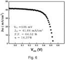
- the CIGS light absorption layer manufactured through Example 1 of the present invention exhibits an excellent energy conversion efficiency.
- the manufacturing method of a CIGS light absorption layer for solar cell using chemical vapor deposition according to the present invention provides a CIGS light absorption layer exhibiting a high energy conversion efficiency by effectively controlling a MoSe x layer.
Landscapes
- Chemical & Material Sciences (AREA)
- General Chemical & Material Sciences (AREA)
- Chemical Kinetics & Catalysis (AREA)
- Engineering & Computer Science (AREA)
- Materials Engineering (AREA)
- Mechanical Engineering (AREA)
- Metallurgy (AREA)
- Organic Chemistry (AREA)
- Inorganic Chemistry (AREA)
- Photovoltaic Devices (AREA)
Applications Claiming Priority (2)
| Application Number | Priority Date | Filing Date | Title |
|---|---|---|---|
| KR1020210060607A KR20220153262A (ko) | 2021-05-11 | 2021-05-11 | 화학기상증착법을 이용한 태양전지용 cigs 광흡수층의 제조방법 |
| PCT/KR2022/006130 WO2022240028A1 (fr) | 2021-05-11 | 2022-04-28 | Procédé de fabrication d'une couche d'absorption de lumière cigs pour cellule solaire par dépôt chimique en phase vapeur |
Publications (2)
| Publication Number | Publication Date |
|---|---|
| EP4340047A1 true EP4340047A1 (fr) | 2024-03-20 |
| EP4340047A4 EP4340047A4 (fr) | 2025-04-30 |
Family
ID=84029254
Family Applications (1)
| Application Number | Title | Priority Date | Filing Date |
|---|---|---|---|
| EP22807676.6A Pending EP4340047A4 (fr) | 2021-05-11 | 2022-04-28 | Procédé de fabrication d'une couche d'absorption de lumière cigs pour cellule solaire par dépôt chimique en phase vapeur |
Country Status (6)
| Country | Link |
|---|---|
| US (1) | US20250160035A1 (fr) |
| EP (1) | EP4340047A4 (fr) |
| JP (1) | JP2024517320A (fr) |
| KR (1) | KR20220153262A (fr) |
| CN (1) | CN117501455A (fr) |
| WO (1) | WO2022240028A1 (fr) |
Family Cites Families (10)
| Publication number | Priority date | Publication date | Assignee | Title |
|---|---|---|---|---|
| US7736940B2 (en) * | 2004-03-15 | 2010-06-15 | Solopower, Inc. | Technique and apparatus for depositing layers of semiconductors for solar cell and module fabrication |
| WO2007121383A2 (fr) * | 2006-04-13 | 2007-10-25 | Solopower, Inc. | Procédé et appareil de formation de couches minces de matériaux sur un support |
| KR101071545B1 (ko) | 2008-12-30 | 2011-10-11 | 주식회사 메카로닉스 | Cigs 박막 제조방법 |
| KR101196350B1 (ko) * | 2011-10-19 | 2012-11-01 | 주식회사 아바코 | 박막형 태양전지와 그 제조 방법 및 이를 제조하기 위한 스퍼터링장치 |
| CN102738299A (zh) * | 2012-06-06 | 2012-10-17 | 华东师范大学 | 一种铜铟镓硒薄膜太阳能电池吸收层的制备方法 |
| KR101389832B1 (ko) * | 2012-11-09 | 2014-04-30 | 한국과학기술연구원 | 구리인듐셀레늄(cigs) 또는 구리아연주석황(czts)계 박막형 태양전지 및 그의 제조방법 |
| KR101482786B1 (ko) * | 2013-04-09 | 2015-01-19 | 한국교통대학교산학협력단 | 산화인듐을 이용한 cigs 광흡수층 제조방법 |
| KR101472409B1 (ko) * | 2013-08-13 | 2014-12-16 | 주식회사 메카로닉스 | 화학적 증착법을 이용한 cis 박막 태양전지의 제조방법 |
| WO2017122842A1 (fr) | 2016-01-13 | 2017-07-20 | 주식회사 메카로 | Cellule solaire comprenant une couche d'absorption de lumière en cigs et son procédé de fabrication |
| KR102227799B1 (ko) * | 2019-02-07 | 2021-03-15 | (주)제이비에이치 | Cigs 박막 태양전지 제조방법 |
-
2021
- 2021-05-11 KR KR1020210060607A patent/KR20220153262A/ko not_active Ceased
-
2022
- 2022-04-28 JP JP2023569923A patent/JP2024517320A/ja active Pending
- 2022-04-28 US US18/558,735 patent/US20250160035A1/en active Pending
- 2022-04-28 WO PCT/KR2022/006130 patent/WO2022240028A1/fr not_active Ceased
- 2022-04-28 EP EP22807676.6A patent/EP4340047A4/fr active Pending
- 2022-04-28 CN CN202280032879.0A patent/CN117501455A/zh active Pending
Also Published As
| Publication number | Publication date |
|---|---|
| WO2022240028A1 (fr) | 2022-11-17 |
| KR20220153262A (ko) | 2022-11-18 |
| JP2024517320A (ja) | 2024-04-19 |
| CN117501455A (zh) | 2024-02-02 |
| EP4340047A4 (fr) | 2025-04-30 |
| US20250160035A1 (en) | 2025-05-15 |
Similar Documents
| Publication | Publication Date | Title |
|---|---|---|
| US8192594B2 (en) | Technique and apparatus for depositing thin layers of semiconductors for solar cell fabrication | |
| US8993882B2 (en) | Chalcogenide-based materials and improved methods of making such materials | |
| US8163090B2 (en) | Methods structures and apparatus to provide group VIA and IA materials for solar cell absorber formation | |
| US7842534B2 (en) | Method for forming a compound semi-conductor thin-film | |
| US20100029038A1 (en) | Manufacturing method of solar cell and manufacturing apparatus of solar cell | |
| US20080305269A1 (en) | Formation of CIGS absorber layer materials using atomic layer deposition and high throughput surface treatment | |
| TW201313936A (zh) | 於基板上形成半導體材料膜層之方法及混合膜層形成裝置 | |
| US20150357486A1 (en) | Solar cell including multiple buffer layer formed by atomic layer deposition and method of fabricating the same | |
| US9905723B2 (en) | Methods for plasma activation of evaporated precursors in a process chamber | |
| CN102544213B (zh) | 制造硫化镉层的方法 | |
| US20250160035A1 (en) | Manufacturing method of cigs light absorption layer for solar cell using chemical vapor deposition | |
| Chae et al. | Ultrafast deposition of microcrystalline Si by thermal plasma chemical vapor deposition | |
| JP6586238B2 (ja) | Cigs光吸収層を含む太陽電池及びその製造方法 | |
| KR101472409B1 (ko) | 화학적 증착법을 이용한 cis 박막 태양전지의 제조방법 | |
| US20100139557A1 (en) | Reactor to form solar cell absorbers in roll-to-roll fashion | |
| CN110819958A (zh) | 一种改变硒化锑薄膜电学性质的方法及硒化锑太阳电池 | |
| KR101867310B1 (ko) | 칼코파이라이트계 박막 태양전지의 제조 방법 | |
| US8632851B1 (en) | Method of forming an I-II-VI2 compound semiconductor thin film of chalcopyrite structure | |
| CN117894881B (zh) | 一种利用多靶溅射调节cigs薄膜或太阳能电池空穴浓度的方法 | |
| WO2010078088A1 (fr) | Réacteur pour former des absorbeurs de cellules solaires selon un mode de rouleau à rouleau | |
| WO2024060423A1 (fr) | Procédé et dispositif de modification de surface pour cellule solaire cigs, et cellule solaire cigs | |
| KR20150136721A (ko) | 고품질 cigs 광흡수층을 포함하는 태양전지 및 이의 제조방법 | |
| KR20150136722A (ko) | 고품질 cigs 광흡수층을 포함하는 태양전지 및 이의 제조방법 | |
| JPH04280417A (ja) | 化合物半導体薄膜の製造方法 | |
| Frijters et al. | Atmospheric spatial atomic-layer-deposition of Zn (O, S) buffer layer for flexible Cu (In, Ga) Se 2 solar cells: From lab-scale to large area roll to roll processing |
Legal Events
| Date | Code | Title | Description |
|---|---|---|---|
| STAA | Information on the status of an ep patent application or granted ep patent |
Free format text: STATUS: THE INTERNATIONAL PUBLICATION HAS BEEN MADE |
|
| PUAI | Public reference made under article 153(3) epc to a published international application that has entered the european phase |
Free format text: ORIGINAL CODE: 0009012 |
|
| STAA | Information on the status of an ep patent application or granted ep patent |
Free format text: STATUS: REQUEST FOR EXAMINATION WAS MADE |
|
| 17P | Request for examination filed |
Effective date: 20231123 |
|
| AK | Designated contracting states |
Kind code of ref document: A1 Designated state(s): AL AT BE BG CH CY CZ DE DK EE ES FI FR GB GR HR HU IE IS IT LI LT LU LV MC MK MT NL NO PL PT RO RS SE SI SK SM TR |
|
| DAV | Request for validation of the european patent (deleted) | ||
| DAX | Request for extension of the european patent (deleted) | ||
| REG | Reference to a national code |
Ref country code: DE Ref legal event code: R079 Free format text: PREVIOUS MAIN CLASS: H01L0031032000 Ipc: H10F0077120000 |
|
| A4 | Supplementary search report drawn up and despatched |
Effective date: 20250327 |
|
| RIC1 | Information provided on ipc code assigned before grant |
Ipc: H01L 21/02 20060101ALI20250324BHEP Ipc: C23C 16/56 20060101ALI20250324BHEP Ipc: C23C 16/30 20060101ALI20250324BHEP Ipc: H10F 77/12 20250101AFI20250324BHEP |