EP4343974B1 - Connecteur - Google Patents
Connecteur Download PDFInfo
- Publication number
- EP4343974B1 EP4343974B1 EP23190478.0A EP23190478A EP4343974B1 EP 4343974 B1 EP4343974 B1 EP 4343974B1 EP 23190478 A EP23190478 A EP 23190478A EP 4343974 B1 EP4343974 B1 EP 4343974B1
- Authority
- EP
- European Patent Office
- Prior art keywords
- insulator
- contact
- retained
- substrate
- connector
- Prior art date
- Legal status (The legal status is an assumption and is not a legal conclusion. Google has not performed a legal analysis and makes no representation as to the accuracy of the status listed.)
- Active
Links
Images




Classifications
-
- H—ELECTRICITY
- H01—ELECTRIC ELEMENTS
- H01R—ELECTRICALLY-CONDUCTIVE CONNECTIONS; STRUCTURAL ASSOCIATIONS OF A PLURALITY OF MUTUALLY-INSULATED ELECTRICAL CONNECTING ELEMENTS; COUPLING DEVICES; CURRENT COLLECTORS
- H01R12/00—Structural associations of a plurality of mutually-insulated electrical connecting elements, specially adapted for printed circuits, e.g. printed circuit boards [PCB], flat or ribbon cables, or like generally planar structures, e.g. terminal strips, terminal blocks; Coupling devices specially adapted for printed circuits, flat or ribbon cables, or like generally planar structures; Terminals specially adapted for contact with, or insertion into, printed circuits, flat or ribbon cables, or like generally planar structures
- H01R12/70—Coupling devices
- H01R12/71—Coupling devices for rigid printing circuits or like structures
- H01R12/712—Coupling devices for rigid printing circuits or like structures co-operating with the surface of the printed circuit or with a coupling device exclusively provided on the surface of the printed circuit
- H01R12/716—Coupling device provided on the PCB
-
- H—ELECTRICITY
- H01—ELECTRIC ELEMENTS
- H01R—ELECTRICALLY-CONDUCTIVE CONNECTIONS; STRUCTURAL ASSOCIATIONS OF A PLURALITY OF MUTUALLY-INSULATED ELECTRICAL CONNECTING ELEMENTS; COUPLING DEVICES; CURRENT COLLECTORS
- H01R12/00—Structural associations of a plurality of mutually-insulated electrical connecting elements, specially adapted for printed circuits, e.g. printed circuit boards [PCB], flat or ribbon cables, or like generally planar structures, e.g. terminal strips, terminal blocks; Coupling devices specially adapted for printed circuits, flat or ribbon cables, or like generally planar structures; Terminals specially adapted for contact with, or insertion into, printed circuits, flat or ribbon cables, or like generally planar structures
- H01R12/70—Coupling devices
- H01R12/71—Coupling devices for rigid printing circuits or like structures
- H01R12/75—Coupling devices for rigid printing circuits or like structures connecting to cables except for flat or ribbon cables
-
- H—ELECTRICITY
- H01—ELECTRIC ELEMENTS
- H01R—ELECTRICALLY-CONDUCTIVE CONNECTIONS; STRUCTURAL ASSOCIATIONS OF A PLURALITY OF MUTUALLY-INSULATED ELECTRICAL CONNECTING ELEMENTS; COUPLING DEVICES; CURRENT COLLECTORS
- H01R12/00—Structural associations of a plurality of mutually-insulated electrical connecting elements, specially adapted for printed circuits, e.g. printed circuit boards [PCB], flat or ribbon cables, or like generally planar structures, e.g. terminal strips, terminal blocks; Coupling devices specially adapted for printed circuits, flat or ribbon cables, or like generally planar structures; Terminals specially adapted for contact with, or insertion into, printed circuits, flat or ribbon cables, or like generally planar structures
- H01R12/50—Fixed connections
- H01R12/59—Fixed connections for flexible printed circuits, flat or ribbon cables or like structures
- H01R12/61—Fixed connections for flexible printed circuits, flat or ribbon cables or like structures connecting to flexible printed circuits, flat or ribbon cables or like structures
-
- H—ELECTRICITY
- H01—ELECTRIC ELEMENTS
- H01R—ELECTRICALLY-CONDUCTIVE CONNECTIONS; STRUCTURAL ASSOCIATIONS OF A PLURALITY OF MUTUALLY-INSULATED ELECTRICAL CONNECTING ELEMENTS; COUPLING DEVICES; CURRENT COLLECTORS
- H01R12/00—Structural associations of a plurality of mutually-insulated electrical connecting elements, specially adapted for printed circuits, e.g. printed circuit boards [PCB], flat or ribbon cables, or like generally planar structures, e.g. terminal strips, terminal blocks; Coupling devices specially adapted for printed circuits, flat or ribbon cables, or like generally planar structures; Terminals specially adapted for contact with, or insertion into, printed circuits, flat or ribbon cables, or like generally planar structures
- H01R12/50—Fixed connections
- H01R12/59—Fixed connections for flexible printed circuits, flat or ribbon cables or like structures
- H01R12/65—Fixed connections for flexible printed circuits, flat or ribbon cables or like structures characterised by the terminal
-
- H—ELECTRICITY
- H01—ELECTRIC ELEMENTS
- H01R—ELECTRICALLY-CONDUCTIVE CONNECTIONS; STRUCTURAL ASSOCIATIONS OF A PLURALITY OF MUTUALLY-INSULATED ELECTRICAL CONNECTING ELEMENTS; COUPLING DEVICES; CURRENT COLLECTORS
- H01R12/00—Structural associations of a plurality of mutually-insulated electrical connecting elements, specially adapted for printed circuits, e.g. printed circuit boards [PCB], flat or ribbon cables, or like generally planar structures, e.g. terminal strips, terminal blocks; Coupling devices specially adapted for printed circuits, flat or ribbon cables, or like generally planar structures; Terminals specially adapted for contact with, or insertion into, printed circuits, flat or ribbon cables, or like generally planar structures
- H01R12/70—Coupling devices
- H01R12/77—Coupling devices for flexible printed circuits, flat or ribbon cables or like structures
- H01R12/81—Coupling devices for flexible printed circuits, flat or ribbon cables or like structures connecting to another cable except for flat or ribbon cable
-
- H—ELECTRICITY
- H01—ELECTRIC ELEMENTS
- H01R—ELECTRICALLY-CONDUCTIVE CONNECTIONS; STRUCTURAL ASSOCIATIONS OF A PLURALITY OF MUTUALLY-INSULATED ELECTRICAL CONNECTING ELEMENTS; COUPLING DEVICES; CURRENT COLLECTORS
- H01R13/00—Details of coupling devices of the kinds covered by groups H01R12/70 or H01R24/00 - H01R33/00
- H01R13/62—Means for facilitating engagement or disengagement of coupling parts or for holding them in engagement
- H01R13/629—Additional means for facilitating engagement or disengagement of coupling parts, e.g. aligning or guiding means, levers, gas pressure electrical locking indicators, manufacturing tolerances
Definitions
- the present invention relates to a connector, particularly to a connector connecting a conductor portion of an electric wire to a conductive portion exposed on a surface of a substrate.
- smart clothes that can obtain user's biological data such as the heart rate and the body temperature only by being worn by the user.
- Such smart clothes have an electrode disposed at a measurement site and constituted of a flexible conductor, and when a wearable device serving as a measurement device is electrically connected to the electrode, biological data can be transmitted to the wearable device.
- the electrode and the wearable device can be interconnected by, for instance, use of a connector connected to the flexible conductor.
- JP 2007-214087 A discloses a connector shown in FIG. 21 as a connector used for connecting an electric wire to a flexible conductor.
- This connector includes a first connector 2 connected to an end of a substrate 1 and a second connector 4 attached to tips of electric wires 3, and the electric wires 3 can be connected to a flexible conductor of the substrate 1 by fitting the second connector 4 to the first connector 2.
- first connector 2 and the second connector 4 that are separately attached to the end of the substrate 1 and the tips of the electric wires 3 need to be fitted to each other in order to connect the electric wires 3 to the flexible conductor of the substrate 1, and this causes a larger size of a device; and there is a separatable connection portion between the first connector 2 and the second connector 4, which impairs the reliability of electric connection.
- a board connector for electrically connecting together circuit boards which are incorporated in, for example, a mobile telephone is known.
- a dust-proof measure is carried out by swingably attaching a cover member to a plug via a fulcrum shaft, and covering contact portions of the plug and socket in a fitting state with the cover member.
- a protrusion which causes an end portion to continuously butt against another one of the plug and the cover member from one end to another end is disposed, whereby, when the plug is inserted, the force of inserting the plug is evenly transmitted from the cover member to the whole plug.
- connection system for flexible flat strip cables having parallel strip conductors lying at a distance from one another which are bared in the contact area, with a first housing part on whose floor is fastened a principal flexible flat strip cable and a second housing part in which a branch flexible flat strip cable is fixed.
- connection structure is known with: conductor exposing parts of the flat wiring material; conductor exposing part of the flexible printed wiring material; and an overlapping connection means for connecting both exposing parts and to each other.
- the present invention has been made to overcome the conventional problems as above and aims at providing a connector that can have a small size while reliably connecting a conductor portion of an electric wire to a conductive portion exposed on a surface of a substrate.
- a connector according to the present invention is one connecting a conductor portion of an electric wire to a conductive portion exposed on a surface of a substrate, the connector comprising:
- FIG. 1 shows a connector 10 according to Embodiment 1.
- the connector 10 is used for connecting a plurality of coated electric wires 12 to a substrate 11 and includes a housing 13 made of an insulating resin material and a plurality of contacts 14 retained by the housing 13.
- the substrate 11 is constituted of a sheet type conductive member, and the connector 10 is mounted on a surface of the substrate 11.
- the coated electric wires 12 are aligned in a predetermined alignment direction and each extend in a direction perpendicular to the alignment direction in parallel to the surface of the substrate 11.
- Each coated electric wire 12 has a structure in which the outer periphery of a conductor portion 12A is covered with an insulating coating portion 12B.
- the conductor portions 12A of the plurality of coated electric wires 12 are electrically connected to a plurality of conductive portions to be described later of the substrate 11.
- the conductor portion 12A of the coated electric wire 12 may be either a so-called solid wire constituted of one conductor or a so-called stranded wire constituted of plural conductors being stranded.
- the housing 13 extends along the alignment direction of the coated electric wires 12.
- the substrate 11 is defined as extending along an XY plane, the alignment direction of the coated electric wires 12 is referred to as "X direction,” the direction in which each coated electric wire 12 extends toward the housing 13 is referred to as "+Y direction,” and the direction perpendicular to an XY plane is referred to as "Z direction.”
- the housing 13 is composed of a first insulator 15 and a second insulator 16 each of which extends in the X direction and which are separate from each other.
- the contacts 14 extending in the Y direction and aligned in the X direction with an alignment pitch P1 are retained by the first insulator 15 and the second insulator 16, and the first insulator 15 and the second insulator 16 are joined together via the contacts 14 with distance from each other in the Y direction.
- the first insulator 15 has a first flat surface 15A facing the +Z direction and extending in an XY plane.
- the first flat surface 15A is provided with a plurality of electric wire insertion grooves 15B aligned in the X direction to correspond to the contacts 14 and each traversing the first insulator 15 in the Y direction, and each electric wire insertion groove 15B is provided at its intermediate portion with a recess portion 15C recessed from the bottom of the electric wire insertion groove 15B toward the -Z direction.
- the recess portions 15C of the electric wire insertion grooves 15B are joined together in the X direction to form a fitting groove 15D extending in the X direction over the entire X directional width of the first insulator 15.
- the bottom surface, facing the -Z direction, of the first insulator 15 is provided with a projection portion 15E extending in the X direction over the entire X directional width of the first insulator 15 and projecting in the -Z direction.
- the second insulator 16 has a second flat surface 16A facing the +Z direction and extending in an XY plane in the state where the contacts 14 each linearly extend in the Y direction such that the first and second insulators 15 and 16 are developed, as shown in FIGS. 2 to 6 .
- the second flat surface 16A is provided with a fitting portion 16B extending in the X direction over the entire X directional width of the second insulator 16 and projecting in the +Z direction, and the fitting portion 16B is provided with a plurality of protrusion portions 16C aligned in the X direction to correspond to the contacts 14 and to be accommodated in the corresponding recess portions 15C of the first insulator 15.
- the first insulator 15 and the second insulator 16 are configured such that, by deforming the contacts 14 to insert the fitting portion 16B of the second insulator 16 into the fitting groove 15D of the first insulator 15, the first insulator 15 and the second insulator 16 are fitted to each other and the second flat surface 16A makes contact with the first flat surface 15A.
- the contact 14 is formed from a band shaped metal sheet substantially extending in the Y direction and having conductivity.
- a mounting portion 14A to be mounted on the substrate 11 is disposed at the -Y directional end of the contact 14, and a first retained portion 14B to be retained by the first insulator 15 is disposed on the +Y direction side of the mounting portion 14A to be adjacent to the mounting portion 14A.
- a second retained portion 14C to be retained by the second insulator 16 is disposed at the +Y directional end of the contact 14, and a joint portion 14D joining together the first retained portion 14B and the second retained portion 14C is disposed between the first retained portion 14B and the second retained portion 14C.
- the first retained portion 14B is provided at its intermediate portion with a recessed bent portion 14E that is bent to be dented in the -Z direction.
- the joint portion 14D is formed to be deformable so as to be curved in the thickness direction of the contact 14; when the connector 10 is assembled, the joint portion 14D is deformed into a U-shape opening toward the -Y direction such that the second retained portion 14C is situated on the +Z direction side of the first retained portion 14B.
- the joint portion 14D is provided at its intermediate portion with a connection portion 14F and an inspection hole 14G.
- the connection portion 14F is formed to project in the -Z direction by lancing the metal plate constituting the contact 14, and the inspection hole 14G is situated on the +Y direction side of the connection portion 14F and penetrates the metal plate constituting the contact 14 in the thickness direction of the contact 14.
- the mounting portion 14A and the connection portion 14F extend in an XY plane in the same Z directional position, and the bottom of the recessed bent portion 14E is situated on the -Z direction side with respect to the Z directional position of the mounting portion 14A and the connection portion 14F.
- the bottom of the recessed bent portion 14E is disposed within the projection portion 15E of the first insulator 15.
- the connector 10 having the thus-configured contacts 14 and the first and second insulators 15 and 16 that are integrally formed is fabricated by, for instance, insert molding.
- the mounting portions 14A situated at the -Y directional ends of the contacts 14 are exposed from the first insulator 15 to project in the -Y direction, and the second retained portions 14C situated at the +Y directional ends of the contacts 14 are embedded in the second insulator 16 such that the second retained portions 14C are not visible from the outside.
- the joint portions 14D of the contacts 14 are exposed between the first insulator 15 and the second insulator 16, and middle portions, in the X direction, of the first retained portions 14B are exposed in the corresponding electric wire insertion grooves 15B of the first insulator 15.
- the recessed bent portions 14E of the contacts 14 are accommodated in the recess portions 15C formed in the intermediate portions of the electric wire insertion grooves 15B such that the inner surfaces of the recessed bent portions 14E are exposed.
- the joint portions 14D of the contacts 14 are deformed into a U-shape and folded back toward the -Y direction while the second insulator 16 is brought up toward the +Z direction with respect to the first insulator 15, thereby having the connector 10 in a pre-assembly state where the second flat surface 16A of the second insulator 16 obliquely faces the first flat surface 15A of the first insulator 15.
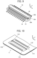
- FIG. 10 shows the substrate 11 on which the connector 10 is to be mounted.
- the substrate 11 is, for instance, constituted of a sheet type conductive member having a multilayer structure in which a plurality of wiring layers each formed from a conductor and a plurality of insulating layers are laminated, and a connector mounting region 11A of rectangular shape is formed on a surface of the substrate 11 on the +Z direction side.
- the connector mounting region 11A is formed by peeling off, in a rectangular shape, an insulating layer 11B disposed at the surface of the substrate 11 on the +Z direction side, and a depression 11C extending in the X direction is formed in a central portion of the connector mounting region 11A. More specifically, the depression 11C is formed from a through-hole penetrating the substrate 11 in the Z direction.
- the depression 11C has a size allowing the projection portion 15E projecting in the -Z direction from the bottom surface of the first insulator 15 to fit therein.
- the inside of the connector mounting region 11A is provided with a plurality of conductive portions 11D aligned in the X direction on the +Y direction side of the depression 11C to correspond to the contacts 14 of the connector 10.
- the conductive portions 11D are formed from part of one wiring layer of the substrate 11 and connected to a plurality of wiring portions (not shown) covered with the insulating layer 11B.
- a plurality of fixing portions 11E aligned in the X direction to correspond to the contacts 14 of the connector 10 are formed on the -Y direction side of the depression 11C in the connector mounting region 11A. While the fixing portions 11E can be formed from part of one wiring layer of the substrate 11 as with the conductive portions 11D, the fixing portions 11E are disposed only in the connector mounting region 11A without being connected to a plurality of wiring portions (not shown).
- the conductive portions 11D and the fixing portions 11E are separately aligned in the X direction with the same pitch as the alignment pitch P1 of the contacts 14.
- the distance between the depression 11C and the conductive portions 11D in the Y direction is substantially the same as the distance between the projection portion 15E of the first insulator 15 and the connection portions 14F of the contacts 14 of the connector 10 in the Y direction
- the distance between the depression 11C and the fixing portions 11E in the Y direction is substantially the same as the distance between the projection portion 15E of the first insulator 15 and the mounting portions 14A of the contacts 14 of the connector 10 in the Y direction.
- connection portions 14F of the contacts 14 are situated on the conductive portions 11D of the substrate 11, and the mounting portions 14A of the contacts 14 are situated on the fixing portions 11E of the substrate 11.
- connection portions 14F and the mounting portions 14A of the contacts 14 are respectively connected to the conductive portions 11D and the fixing portions 11E of the substrate 11 by soldering or other methods, whereby the connector 10 is mounted on the substrate 11.
- the coated electric wires 12 are aligned in the X direction, and the conductor portions 12A drawn from the coated electric wires 12 are inserted into the first insulator 15 of the connector 10 from the -Y direction, as shown in FIG. 12 .
- each conductor portion 12A is inserted into the corresponding electric wire insertion groove 15B of the first insulator 15 as shown in FIG. 13 . Since the first retained portion 14B of the contact 14 is exposed in the electric wire insertion groove 15B, the conductor portion 12A is disposed on a surface of the first retained portion 14B of the contact 14 as shown in FIG. 14 . The conductor portion 12A is inserted into the electric wire insertion groove 15B until the +Y directional end of the conductor portion 12A protrudes on the +Y direction side of the first insulator 15 and reaches a position near the connection portion 14F of the contact 14 on the +Z direction side of the contact 14.
- the inspection hole 14G formed in the joint portion 14D of the contact 14 is situated on the +Z direction side of the connection portion 14F in the connector 10 in the pre-assembly state where the joint portion 14D of the contact 14 is deformed in a U-shape such that the second flat surface 16A of the second insulator 16 obliquely faces the first flat surface 15A of the first insulator 15.
- an operator carrying out the connecting operation of the coated electric wires 12 can visually check that the +Y directional ends of the conductor portions 12A protrude on the +Y direction side of the first insulator 15 by a predetermined length through the inspection holes 14G of the contacts 14.
- the reliability of electric connection between the conductor portion 12A and the contact 14 may decrease; when the insertion length of the conductor portion 12A is excessively large, one conductor portion 12A may be short-circuited with a contact 14 corresponding to an adjacent conductor portion 12A.
- the reliability of connection of the coated electric wires 12 can be improved by checking the +Y directional ends of the conductor portions 12A inserted up to the proper positions.
- the second insulator 16 is pressed against the first insulator 15 in the -Z direction and thereby fitted to the first insulator 15 as shown in FIG. 16 .
- the second flat surface 16A of the second insulator 16 makes contact with the first flat surface 15A of the first insulator 15, and a middle portion of the conductor portion 12A inserted in the electric wire insertion groove 15B of the first insulator 15 is pushed into the recessed bent portion 14E of the contact 14 accommodated in the corresponding recess portion 15C of the first insulator 15 by the protrusion portion 16C of the second insulator 16.
- the conductor portion 12A of the coated electric wire 12 and the recessed bent portion 14E of the contact 14 make contact with each other in the Y direction with a predetermined contact pressure between the inner lateral surface of the recess portion 15C and the outer lateral surface of the protrusion portion 16C, so that the conductor portion 12A is electrically connected to the recessed bent portion 14E of the contact 14.
- the connection portion 14F of the contact 14 is connected to the corresponding conductive portion 11D of the substrate 11
- the conductor portion 12A of the coated electric wire 12 is electrically connected to the conductive portion 11D of the substrate 11 via the contact 14.
- the conductor portion 12A of the coated electric wire 12 is pushed into the recessed bent portion 14E of the contact 14 and thereby bent along the inner surface of the recessed bent portion 14E; accordingly, the +Y directional end of the conductor portion 12A is retracted in the -Y direction and accommodated within the electric wire insertion groove 15B of the first insulator 15.
- an operator cannot visually recognize the +Y directional end of the conductor portion 12A even when looking in the inspection hole 14G of the contact 14 from the +Z direction, as shown in FIG. 17 .
- the operator can confirm that the conductor portions 12A have been properly pushed in the recessed bent portions 14E of the contacts 14 and electrically connected to the contacts 14 based on the fact that the +Y directional ends of the conductor portions 12A are not seen through the inspection holes 14G of the contacts 14.
- a locking portion 15F projecting toward the middle of the first insulator 15 in the X direction is formed at each of the +X directional end and the -X directional end of the first insulator 15, and likewise, a locked portion 16E corresponding to the locking portion 15F of the first insulator 15 is formed at each of the +X directional end and the -X directional end of the second insulator 16.
- the locking portions 15F and the locked portions 16E interfere with each other, thereby maintaining the fitting state between the first insulator 15 and the second insulator 16.
- the recessed bent portion 14E of the contact 14 has a sufficient length in the Z direction such that the bottom of the recessed bent portion 14E is situated on the -Z direction side with respect to the mounting portion 14A and the connection portion 14F, and owing to this configuration, the contact area can be ensured between the inner lateral surface of the recessed bent portion 14E and the conductor portion 12A that make contact in the Y direction, thus making it possible to electrically connect the conductor portion 12A to the contact 14 with high reliability.
- the bottom of the recessed bent portion 14E of the contact 14 is disposed inside the projection portion 15E of the first insulator 15, and the projection portion 15E is inserted in the depression 11C of the substrate 11; therefore, the connector 10 with a small thickness can be obtained despite the recessed bent portion 14E having a sufficient length in the Z direction.
- FIG. 19 shows a connector 20 according to Embodiment 2.
- the connector 20 is configured to use a contact 24 in place of the contact 14 in the connector 10 of Embodiment 1. Specifically, the first insulator 15 and the second insulator 16 are joined together by a plurality of contacts 24 with distance.
- the contact 24 is formed from a band shaped metal sheet having conductivity as with the contact 14 shown in FIGS. 7 and 8 and includes a mounting portion 24A disposed at the -Y directional end of the contact 24, a first retained portion 24B situated on the +Y direction side of the mounting portion 24A to be adjacent to the mounting portion 24A and retained by the first insulator 15, and a joint portion 24D situated on the +Y direction side of the first retained portion 24B to be adjacent to the first retained portion 24B and exposed.
- a recessed bent portion 24E is formed at an intermediate portion of the first retained portion 24B
- a connection portion 24F is formed at an intermediate portion of the joint portion 24D.
- the mounting portion 24A, the first retained portion 24B, the joint portion 24D, the recessed bent portion 24E, and the connection portion 24F have the same structures as those of the mounting portion 14A, the first retained portion 14B, the joint portion 14D, the recessed bent portion 14E, and the connection portion 14F of the contact 14 in the connector 10 of Embodiment 1.
- the contact 24 further includes a second retained portion 24C joined to the joint portion 24D and retained by the second insulator 16, and the second retained portion 24C includes a protruding bent portion 24H extending along the outer surface of the protrusion portion 16C of the second insulator 16 and exposed.
- the recessed bent portion 14E, 24E of the contact 14, 24 makes contact with the conductor portion 12A of the coated electric wire 12 with a predetermined contact pressure in the Y direction in Embodiments 1 and 2 above, the recessed bent portion 14E, 24E may have a spring property that presses the conductor portion 12A in the Y direction.
- the connector 10, 20 is formed by insert molding in Embodiments 1 and 2, the connector 10, 20 may be formed by, for instance, press-fitting the contacts 14, 24 such that the contacts 14, 24 are retained by both the first insulator 15 and the second insulator 16.
- the substrate 11 is constituted of a sheet type conductive member, and either a flexible substrate or a rigid substrate may be used as the substrate 11. Furthermore, the substrate 11 is not limited to a sheet type conductive member as long as it has the connector mounting region 11A used for mounting the connector 10, 20.
- the depression 11C of the substrate 11 is formed from a through-hole penetrating the substrate 11 in the Z direction in Embodiments 1 and 2, the depression 11C may be constituted of a recess formed at the surface of the substrate 11 on the +Z direction side without penetrating the substrate 11 when the substrate 11 has a sufficient thickness.
- the invention is not limited thereto, and a connector may be configured such that a single coated electric wire 12 is connected to the substrate 11 in the same manner.
- coated electric wire 12 is used as an electric wire connected to the substrate 11, an electric wire constituted only of the conductor portion 12A whose outer periphery is not covered with the insulating coating portion 12B may be connected to the substrate 11.
Landscapes
- Coupling Device And Connection With Printed Circuit (AREA)
- Connector Housings Or Holding Contact Members (AREA)
Claims (11)
- Connecteur (10, 20) connectant une partie conductrice (12A) d'un fil électrique (12) à une partie conductible (11D) exposée sur une surface d'un substrat (11), le connecteur comprenant :un premier isolateur (15) disposé sur la surface du substrat et présentant une partie en retrait (15C) ;un second isolateur (16) disposé de manière à pouvoir être ajusté avec le premier isolateur et présentant une partie en saillie (16C) correspondant à la partie en retrait ; etun contact (14, 24) ayant une conductivité et retenu à la fois par le premier isolateur et le second isolateur,le contact (14, 24) comportant :une partie de montage (14A, 24A) située à une extrémité du contact et montée sur le substrat ;une première partie retenue (14B, 24B) située de manière à être adjacente à la partie de montage et retenue par le premier isolateur ;une seconde partie retenue (14C, 24C) située à l'autre extrémité du contact et retenue par le second isolateur ;une partie de jonction (14D, 24D) joignant la première partie retenue et la seconde partie retenue et pouvant être déformée ; etune partie de connexion (14F, 24F) connectée électriquement à la partie conductible du substrat, dans lequel la première partie retenue comporte une partie pliée en retrait (14E, 24E) qui est logée dans la partie en retrait et s'étend le long d'une surface intérieure de la partie en retrait,le premier isolateur et le second isolateur sont ajustés l'un à l'autre de sorte que la partie conductrice du fil électrique est prise en sandwich entre la partie pliée en retrait du contact et la partie en saillie du second isolateur, etla partie conductrice du fil électrique entre en contact avec la partie pliée en retrait entre la partie en retrait et la partie en saillie, de sorte que la partie conductrice du fil électrique est connectée électriquement à la partie conductible du substrat par l'intermédiaire du contact.
- Connecteur selon la revendication 1,
dans lequel la partie conductrice (12A) du fil électrique et la partie pliée en retrait (14E, 24E) du contact entrent en contact l'une avec l'autre avec une pression de contact prédéterminée entre une surface latérale intérieure de la partie en retrait (15C) et une surface latérale extérieure de la partie en saillie (16C). - Connecteur selon la revendication 1 ou 2,
dans lequel la partie de jonction (14D, 24D) du contact est courbée en forme de U dans un état d'ajustement où le premier isolateur est ajusté avec le second isolateur. - Connecteur selon la revendication 3,
dans lequel la partie de jonction (14D) présente un trou d'inspection (14G) qui pénètre le contact dans une direction d'épaisseur du contact et permet un contrôle visuel d'une pointe de la partie conductrice du fil électrique. - Connecteur selon l'une quelconque des revendications 1 à 4,dans lequel le premier isolateur (15) comporte une partie protubérante (15E) dépassant vers la surface du substrat, une dépression (11C) est formée à la surface du substrat (11), etle premier isolateur est disposé sur la surface du substrat, la partie protubérante étant logée dans la dépression.
- Connecteur selon l'une quelconque des revendications 1 à 5,
dans lequel la seconde partie retenue (24C) du contact (24) comporte une partie pliée en saillie (24H) s'étendant le long d'une surface extérieure de la partie en saillie, et la partie conductrice (12A) du fil électrique est prise en sandwich entre la partie pliée en retrait (24E) et la partie pliée en saillie (24H) du contact et entre en contact à la fois avec la partie pliée en retrait et la partie pliée en saillie. - Connecteur selon l'une quelconque des revendications 1 à 6,
dans lequel la partie de connexion (14F, 24F) est disposée dans la partie de jonction (14D, 24D). - Connecteur selon l'une quelconque des revendications 1 à 7,
dans lequel le contact (14, 24) est formé dans le premier isolateur (15) et le second isolateur (16) par moulage par insertion. - Connecteur selon l'une quelconque des revendications 1 à 8, comprenant une pluralité des contacts (14, 24) alignés dans une direction d'alignement prédéterminée et chacun retenu à la fois par le premier isolateur et le second isolateur,
dans lequel les parties conductrices (12A) d'une pluralité des fils électriques (12) sont connectées électriquement à une pluralité des parties conductibles du substrat par l'intermédiaire de la pluralité de contacts. - Connecteur selon la revendication 9, comprenant un mécanisme de verrouillage utilisé pour maintenir un état d'ajustement entre le premier isolateur et le second isolateur.
- Connecteur selon la revendication 10,
dans lequel le mécanisme de verrouillage est composé d'une partie de verrouillage (15F) disposée dans le premier isolateur et d'une partie verrouillée (16E) disposée dans le second isolateur.
Applications Claiming Priority (1)
| Application Number | Priority Date | Filing Date | Title |
|---|---|---|---|
| JP2022152679A JP7837843B2 (ja) | 2022-09-26 | 2022-09-26 | コネクタ |
Publications (2)
| Publication Number | Publication Date |
|---|---|
| EP4343974A1 EP4343974A1 (fr) | 2024-03-27 |
| EP4343974B1 true EP4343974B1 (fr) | 2025-01-22 |
Family
ID=87567502
Family Applications (1)
| Application Number | Title | Priority Date | Filing Date |
|---|---|---|---|
| EP23190478.0A Active EP4343974B1 (fr) | 2022-09-26 | 2023-08-09 | Connecteur |
Country Status (3)
| Country | Link |
|---|---|
| EP (1) | EP4343974B1 (fr) |
| JP (1) | JP7837843B2 (fr) |
| CN (1) | CN117767046A (fr) |
Family Cites Families (9)
| Publication number | Priority date | Publication date | Assignee | Title |
|---|---|---|---|---|
| US4555155A (en) | 1983-11-28 | 1985-11-26 | Minnesota Mining And Manufacturing Company | Bioelectrode connector |
| DE68918080T2 (de) * | 1989-04-14 | 1995-03-16 | Whitaker Corp | Gehäuse in Kombination mit einem Verbinder eines flachen Starkstromkabels. |
| DE10115283C1 (de) * | 2001-03-28 | 2002-10-02 | Fci Automotive Deutschland Gmb | Flex-Verbindungsanordnung mit Federgehäuse |
| JP2004063280A (ja) * | 2002-07-29 | 2004-02-26 | Furukawa Electric Co Ltd:The | 平型配線材とフレキシブルプリント配線材の接続構造及びその製造方法 |
| JP4386676B2 (ja) | 2003-05-30 | 2009-12-16 | スリーエム イノベイティブ プロパティズ カンパニー | コネクタ |
| JP4521351B2 (ja) | 2005-10-17 | 2010-08-11 | ホシデン株式会社 | 基板用コネクタ |
| JP2007214087A (ja) | 2006-02-13 | 2007-08-23 | Fujikura Ltd | コネクタ |
| CN201044282Y (zh) | 2007-04-20 | 2008-04-02 | 达昌电子科技(苏州)有限公司 | 软性排线连接器 |
| JP6864255B2 (ja) | 2017-03-01 | 2021-04-28 | 三菱自動車工業株式会社 | 電動車両のバッテリパック |
-
2022
- 2022-09-26 JP JP2022152679A patent/JP7837843B2/ja active Active
-
2023
- 2023-08-01 CN CN202310962176.4A patent/CN117767046A/zh active Pending
- 2023-08-09 EP EP23190478.0A patent/EP4343974B1/fr active Active
Also Published As
| Publication number | Publication date |
|---|---|
| JP2024047190A (ja) | 2024-04-05 |
| US20240106143A1 (en) | 2024-03-28 |
| EP4343974A1 (fr) | 2024-03-27 |
| JP7837843B2 (ja) | 2026-03-31 |
| CN117767046A (zh) | 2024-03-26 |
Similar Documents
| Publication | Publication Date | Title |
|---|---|---|
| JP7208115B2 (ja) | コネクタ | |
| CN102195162B (zh) | 连接器装置 | |
| US7351096B2 (en) | Cable connector | |
| US10630004B2 (en) | Connection assisting member and circuit board assembly | |
| US20040185708A1 (en) | Connector and cable positioning member of connector | |
| JP2002203645A (ja) | ケーブルコネクタ | |
| US8942007B2 (en) | Electrical component | |
| US11431123B2 (en) | Connector having holding member for holding conductive member | |
| US12424774B2 (en) | Connector | |
| US6309223B1 (en) | Terminal assembly for flexible circuit strip | |
| EP4213308B1 (fr) | Connecteur | |
| CN103682889A (zh) | 适于平板状连接物体的连接的同轴连接器 | |
| EP4343974B1 (fr) | Connecteur | |
| US10862254B2 (en) | Coated conductive wire connecting method, coated conductive wire connecting structure and coated conductive wire connecting member | |
| US12567689B2 (en) | Connector assembly and connecting method | |
| US12620740B2 (en) | Connector connecting an electric wire to a substrate | |
| EP4346013B1 (fr) | Connecteur, ensemble connecteur et procédé de connexion | |
| JP3977636B2 (ja) | 平型柔軟ケーブル用コネクタ | |
| JP2863766B2 (ja) | コネクタ | |
| JP7562768B2 (ja) | コネクタ | |
| JPH1032062A (ja) | 電気コネクタ | |
| KR101160901B1 (ko) | 한쌍의 헤더 콘택트 및 이것을 이용한 헤더 커넥터 | |
| JP2024085525A (ja) | コネクタ | |
| JPH10270106A (ja) | コネクタ装着構造 | |
| US20050129369A1 (en) | Multiconductor surface-mount connector for printed-circuit board |
Legal Events
| Date | Code | Title | Description |
|---|---|---|---|
| PUAI | Public reference made under article 153(3) epc to a published international application that has entered the european phase |
Free format text: ORIGINAL CODE: 0009012 |
|
| STAA | Information on the status of an ep patent application or granted ep patent |
Free format text: STATUS: REQUEST FOR EXAMINATION WAS MADE |
|
| 17P | Request for examination filed |
Effective date: 20230809 |
|
| AK | Designated contracting states |
Kind code of ref document: A1 Designated state(s): AL AT BE BG CH CY CZ DE DK EE ES FI FR GB GR HR HU IE IS IT LI LT LU LV MC ME MK MT NL NO PL PT RO RS SE SI SK SM TR |
|
| RBV | Designated contracting states (corrected) |
Designated state(s): AL AT BE BG CH CY CZ DE DK EE ES FI FR GB GR HR HU IE IS IT LI LT LU LV MC ME MK MT NL NO PL PT RO RS SE SI SK SM TR |
|
| GRAP | Despatch of communication of intention to grant a patent |
Free format text: ORIGINAL CODE: EPIDOSNIGR1 |
|
| STAA | Information on the status of an ep patent application or granted ep patent |
Free format text: STATUS: GRANT OF PATENT IS INTENDED |
|
| RAP3 | Party data changed (applicant data changed or rights of an application transferred) |
Owner name: JAPAN AVIATION ELECTRONICS INDUSTRY, LIMITED |
|
| INTG | Intention to grant announced |
Effective date: 20241015 |
|
| GRAS | Grant fee paid |
Free format text: ORIGINAL CODE: EPIDOSNIGR3 |
|
| GRAA | (expected) grant |
Free format text: ORIGINAL CODE: 0009210 |
|
| STAA | Information on the status of an ep patent application or granted ep patent |
Free format text: STATUS: THE PATENT HAS BEEN GRANTED |
|
| AK | Designated contracting states |
Kind code of ref document: B1 Designated state(s): AL AT BE BG CH CY CZ DE DK EE ES FI FR GB GR HR HU IE IS IT LI LT LU LV MC ME MK MT NL NO PL PT RO RS SE SI SK SM TR |
|
| REG | Reference to a national code |
Ref country code: GB Ref legal event code: FG4D |
|
| REG | Reference to a national code |
Ref country code: CH Ref legal event code: EP |
|
| REG | Reference to a national code |
Ref country code: IE Ref legal event code: FG4D |
|
| REG | Reference to a national code |
Ref country code: DE Ref legal event code: R096 Ref document number: 602023001757 Country of ref document: DE |
|
| REG | Reference to a national code |
Ref country code: NL Ref legal event code: MP Effective date: 20250122 |
|
| PG25 | Lapsed in a contracting state [announced via postgrant information from national office to epo] |
Ref country code: NL Free format text: LAPSE BECAUSE OF FAILURE TO SUBMIT A TRANSLATION OF THE DESCRIPTION OR TO PAY THE FEE WITHIN THE PRESCRIBED TIME-LIMIT Effective date: 20250122 |
|
| PG25 | Lapsed in a contracting state [announced via postgrant information from national office to epo] |
Ref country code: RS Free format text: LAPSE BECAUSE OF FAILURE TO SUBMIT A TRANSLATION OF THE DESCRIPTION OR TO PAY THE FEE WITHIN THE PRESCRIBED TIME-LIMIT Effective date: 20250422 |
|
| PG25 | Lapsed in a contracting state [announced via postgrant information from national office to epo] |
Ref country code: FI Free format text: LAPSE BECAUSE OF FAILURE TO SUBMIT A TRANSLATION OF THE DESCRIPTION OR TO PAY THE FEE WITHIN THE PRESCRIBED TIME-LIMIT Effective date: 20250122 |
|
| PG25 | Lapsed in a contracting state [announced via postgrant information from national office to epo] |
Ref country code: PL Free format text: LAPSE BECAUSE OF FAILURE TO SUBMIT A TRANSLATION OF THE DESCRIPTION OR TO PAY THE FEE WITHIN THE PRESCRIBED TIME-LIMIT Effective date: 20250122 |
|
| PG25 | Lapsed in a contracting state [announced via postgrant information from national office to epo] |
Ref country code: ES Free format text: LAPSE BECAUSE OF FAILURE TO SUBMIT A TRANSLATION OF THE DESCRIPTION OR TO PAY THE FEE WITHIN THE PRESCRIBED TIME-LIMIT Effective date: 20250122 |
|
| REG | Reference to a national code |
Ref country code: LT Ref legal event code: MG9D |
|
| PG25 | Lapsed in a contracting state [announced via postgrant information from national office to epo] |
Ref country code: IS Free format text: LAPSE BECAUSE OF FAILURE TO SUBMIT A TRANSLATION OF THE DESCRIPTION OR TO PAY THE FEE WITHIN THE PRESCRIBED TIME-LIMIT Effective date: 20250522 Ref country code: NO Free format text: LAPSE BECAUSE OF FAILURE TO SUBMIT A TRANSLATION OF THE DESCRIPTION OR TO PAY THE FEE WITHIN THE PRESCRIBED TIME-LIMIT Effective date: 20250422 |
|
| REG | Reference to a national code |
Ref country code: AT Ref legal event code: MK05 Ref document number: 1762185 Country of ref document: AT Kind code of ref document: T Effective date: 20250122 |
|
| PG25 | Lapsed in a contracting state [announced via postgrant information from national office to epo] |
Ref country code: HR Free format text: LAPSE BECAUSE OF FAILURE TO SUBMIT A TRANSLATION OF THE DESCRIPTION OR TO PAY THE FEE WITHIN THE PRESCRIBED TIME-LIMIT Effective date: 20250122 |
|
| PG25 | Lapsed in a contracting state [announced via postgrant information from national office to epo] |
Ref country code: LV Free format text: LAPSE BECAUSE OF FAILURE TO SUBMIT A TRANSLATION OF THE DESCRIPTION OR TO PAY THE FEE WITHIN THE PRESCRIBED TIME-LIMIT Effective date: 20250122 Ref country code: PT Free format text: LAPSE BECAUSE OF FAILURE TO SUBMIT A TRANSLATION OF THE DESCRIPTION OR TO PAY THE FEE WITHIN THE PRESCRIBED TIME-LIMIT Effective date: 20250522 |
|
| PG25 | Lapsed in a contracting state [announced via postgrant information from national office to epo] |
Ref country code: BG Free format text: LAPSE BECAUSE OF FAILURE TO SUBMIT A TRANSLATION OF THE DESCRIPTION OR TO PAY THE FEE WITHIN THE PRESCRIBED TIME-LIMIT Effective date: 20250122 Ref country code: GR Free format text: LAPSE BECAUSE OF FAILURE TO SUBMIT A TRANSLATION OF THE DESCRIPTION OR TO PAY THE FEE WITHIN THE PRESCRIBED TIME-LIMIT Effective date: 20250423 |
|
| PG25 | Lapsed in a contracting state [announced via postgrant information from national office to epo] |
Ref country code: AT Free format text: LAPSE BECAUSE OF FAILURE TO SUBMIT A TRANSLATION OF THE DESCRIPTION OR TO PAY THE FEE WITHIN THE PRESCRIBED TIME-LIMIT Effective date: 20250122 |
|
| PG25 | Lapsed in a contracting state [announced via postgrant information from national office to epo] |
Ref country code: SE Free format text: LAPSE BECAUSE OF FAILURE TO SUBMIT A TRANSLATION OF THE DESCRIPTION OR TO PAY THE FEE WITHIN THE PRESCRIBED TIME-LIMIT Effective date: 20250122 |
|
| PG25 | Lapsed in a contracting state [announced via postgrant information from national office to epo] |
Ref country code: SM Free format text: LAPSE BECAUSE OF FAILURE TO SUBMIT A TRANSLATION OF THE DESCRIPTION OR TO PAY THE FEE WITHIN THE PRESCRIBED TIME-LIMIT Effective date: 20250122 |
|
| PG25 | Lapsed in a contracting state [announced via postgrant information from national office to epo] |
Ref country code: DK Free format text: LAPSE BECAUSE OF FAILURE TO SUBMIT A TRANSLATION OF THE DESCRIPTION OR TO PAY THE FEE WITHIN THE PRESCRIBED TIME-LIMIT Effective date: 20250122 |
|
| PGFP | Annual fee paid to national office [announced via postgrant information from national office to epo] |
Ref country code: DE Payment date: 20250821 Year of fee payment: 3 |
|
| PG25 | Lapsed in a contracting state [announced via postgrant information from national office to epo] |
Ref country code: IT Free format text: LAPSE BECAUSE OF FAILURE TO SUBMIT A TRANSLATION OF THE DESCRIPTION OR TO PAY THE FEE WITHIN THE PRESCRIBED TIME-LIMIT Effective date: 20250122 |
|
| PGFP | Annual fee paid to national office [announced via postgrant information from national office to epo] |
Ref country code: FR Payment date: 20250828 Year of fee payment: 3 |
|
| PG25 | Lapsed in a contracting state [announced via postgrant information from national office to epo] |
Ref country code: EE Free format text: LAPSE BECAUSE OF FAILURE TO SUBMIT A TRANSLATION OF THE DESCRIPTION OR TO PAY THE FEE WITHIN THE PRESCRIBED TIME-LIMIT Effective date: 20250122 Ref country code: CZ Free format text: LAPSE BECAUSE OF FAILURE TO SUBMIT A TRANSLATION OF THE DESCRIPTION OR TO PAY THE FEE WITHIN THE PRESCRIBED TIME-LIMIT Effective date: 20250122 |
|
| REG | Reference to a national code |
Ref country code: DE Ref legal event code: R097 Ref document number: 602023001757 Country of ref document: DE |
|
| PG25 | Lapsed in a contracting state [announced via postgrant information from national office to epo] |
Ref country code: RO Free format text: LAPSE BECAUSE OF FAILURE TO SUBMIT A TRANSLATION OF THE DESCRIPTION OR TO PAY THE FEE WITHIN THE PRESCRIBED TIME-LIMIT Effective date: 20250122 |
|
| PG25 | Lapsed in a contracting state [announced via postgrant information from national office to epo] |
Ref country code: SK Free format text: LAPSE BECAUSE OF FAILURE TO SUBMIT A TRANSLATION OF THE DESCRIPTION OR TO PAY THE FEE WITHIN THE PRESCRIBED TIME-LIMIT Effective date: 20250122 |
|
| PLBE | No opposition filed within time limit |
Free format text: ORIGINAL CODE: 0009261 |
|
| STAA | Information on the status of an ep patent application or granted ep patent |
Free format text: STATUS: NO OPPOSITION FILED WITHIN TIME LIMIT |
|
| 26N | No opposition filed |
Effective date: 20251023 |
|
| PG25 | Lapsed in a contracting state [announced via postgrant information from national office to epo] |
Ref country code: MC Free format text: LAPSE BECAUSE OF FAILURE TO SUBMIT A TRANSLATION OF THE DESCRIPTION OR TO PAY THE FEE WITHIN THE PRESCRIBED TIME-LIMIT Effective date: 20250122 |
|
| PG25 | Lapsed in a contracting state [announced via postgrant information from national office to epo] |
Ref country code: LU Free format text: LAPSE BECAUSE OF NON-PAYMENT OF DUE FEES Effective date: 20250809 |