EP4345919A1 - Lichtzündbarer thyristor und verfahren zu seiner herstellung - Google Patents
Lichtzündbarer thyristor und verfahren zu seiner herstellung Download PDFInfo
- Publication number
- EP4345919A1 EP4345919A1 EP23199813.9A EP23199813A EP4345919A1 EP 4345919 A1 EP4345919 A1 EP 4345919A1 EP 23199813 A EP23199813 A EP 23199813A EP 4345919 A1 EP4345919 A1 EP 4345919A1
- Authority
- EP
- European Patent Office
- Prior art keywords
- layer
- type conductivity
- ranges
- gallium nitride
- thyristor
- Prior art date
- Legal status (The legal status is an assumption and is not a legal conclusion. Google has not performed a legal analysis and makes no representation as to the accuracy of the status listed.)
- Pending
Links
Images


Classifications
-
- H—ELECTRICITY
- H10—SEMICONDUCTOR DEVICES; ELECTRIC SOLID-STATE DEVICES NOT OTHERWISE PROVIDED FOR
- H10F—INORGANIC SEMICONDUCTOR DEVICES SENSITIVE TO INFRARED RADIATION, LIGHT, ELECTROMAGNETIC RADIATION OF SHORTER WAVELENGTH OR CORPUSCULAR RADIATION
- H10F30/00—Individual radiation-sensitive semiconductor devices in which radiation controls the flow of current through the devices, e.g. photodetectors
- H10F30/20—Individual radiation-sensitive semiconductor devices in which radiation controls the flow of current through the devices, e.g. photodetectors the devices having potential barriers, e.g. phototransistors
- H10F30/21—Individual radiation-sensitive semiconductor devices in which radiation controls the flow of current through the devices, e.g. photodetectors the devices having potential barriers, e.g. phototransistors the devices being sensitive to infrared, visible or ultraviolet radiation
- H10F30/26—Individual radiation-sensitive semiconductor devices in which radiation controls the flow of current through the devices, e.g. photodetectors the devices having potential barriers, e.g. phototransistors the devices being sensitive to infrared, visible or ultraviolet radiation the devices having three or more potential barriers, e.g. photothyristors
- H10F30/263—Photothyristors
-
- H—ELECTRICITY
- H10—SEMICONDUCTOR DEVICES; ELECTRIC SOLID-STATE DEVICES NOT OTHERWISE PROVIDED FOR
- H10P—GENERIC PROCESSES OR APPARATUS FOR THE MANUFACTURE OR TREATMENT OF DEVICES COVERED BY CLASS H10
- H10P14/00—Formation of materials, e.g. in the shape of layers or pillars
- H10P14/20—Formation of materials, e.g. in the shape of layers or pillars of semiconductor materials
-
- H—ELECTRICITY
- H10—SEMICONDUCTOR DEVICES; ELECTRIC SOLID-STATE DEVICES NOT OTHERWISE PROVIDED FOR
- H10D—INORGANIC ELECTRIC SEMICONDUCTOR DEVICES
- H10D62/00—Semiconductor bodies, or regions thereof, of devices having potential barriers
- H10D62/80—Semiconductor bodies, or regions thereof, of devices having potential barriers characterised by the materials
- H10D62/81—Semiconductor bodies, or regions thereof, of devices having potential barriers characterised by the materials of structures exhibiting quantum-confinement effects, e.g. single quantum wells; of structures having periodic or quasi-periodic potential variation
-
- H—ELECTRICITY
- H10—SEMICONDUCTOR DEVICES; ELECTRIC SOLID-STATE DEVICES NOT OTHERWISE PROVIDED FOR
- H10D—INORGANIC ELECTRIC SEMICONDUCTOR DEVICES
- H10D84/00—Integrated devices formed in or on semiconductor substrates that comprise only semiconducting layers, e.g. on Si wafers or on GaAs-on-Si wafers
- H10D84/01—Manufacture or treatment
- H10D84/0112—Integrating together multiple components covered by H10D8/00, H10D10/00 or H10D18/00, e.g. integrating multiple BJTs
-
- H—ELECTRICITY
- H10—SEMICONDUCTOR DEVICES; ELECTRIC SOLID-STATE DEVICES NOT OTHERWISE PROVIDED FOR
- H10D—INORGANIC ELECTRIC SEMICONDUCTOR DEVICES
- H10D84/00—Integrated devices formed in or on semiconductor substrates that comprise only semiconducting layers, e.g. on Si wafers or on GaAs-on-Si wafers
- H10D84/01—Manufacture or treatment
- H10D84/02—Manufacture or treatment characterised by using material-based technologies
- H10D84/03—Manufacture or treatment characterised by using material-based technologies using Group IV technology, e.g. silicon technology or silicon-carbide [SiC] technology
- H10D84/038—Manufacture or treatment characterised by using material-based technologies using Group IV technology, e.g. silicon technology or silicon-carbide [SiC] technology using silicon technology, e.g. SiGe
-
- H—ELECTRICITY
- H10—SEMICONDUCTOR DEVICES; ELECTRIC SOLID-STATE DEVICES NOT OTHERWISE PROVIDED FOR
- H10F—INORGANIC SEMICONDUCTOR DEVICES SENSITIVE TO INFRARED RADIATION, LIGHT, ELECTROMAGNETIC RADIATION OF SHORTER WAVELENGTH OR CORPUSCULAR RADIATION
- H10F39/00—Integrated devices, or assemblies of multiple devices, comprising at least one element covered by group H10F30/00, e.g. radiation detectors comprising photodiode arrays
- H10F39/10—Integrated devices
-
- H—ELECTRICITY
- H10—SEMICONDUCTOR DEVICES; ELECTRIC SOLID-STATE DEVICES NOT OTHERWISE PROVIDED FOR
- H10F—INORGANIC SEMICONDUCTOR DEVICES SENSITIVE TO INFRARED RADIATION, LIGHT, ELECTROMAGNETIC RADIATION OF SHORTER WAVELENGTH OR CORPUSCULAR RADIATION
- H10F71/00—Manufacture or treatment of devices covered by this subclass
- H10F71/127—The active layers comprising only Group III-V materials, e.g. GaAs or InP
- H10F71/1278—The active layers comprising only Group III-V materials, e.g. GaAs or InP comprising nitrides, e.g. GaN
-
- H—ELECTRICITY
- H10—SEMICONDUCTOR DEVICES; ELECTRIC SOLID-STATE DEVICES NOT OTHERWISE PROVIDED FOR
- H10F—INORGANIC SEMICONDUCTOR DEVICES SENSITIVE TO INFRARED RADIATION, LIGHT, ELECTROMAGNETIC RADIATION OF SHORTER WAVELENGTH OR CORPUSCULAR RADIATION
- H10F77/00—Constructional details of devices covered by this subclass
- H10F77/10—Semiconductor bodies
- H10F77/12—Active materials
- H10F77/124—Active materials comprising only Group III-V materials, e.g. GaAs
- H10F77/1248—Active materials comprising only Group III-V materials, e.g. GaAs having three or more elements, e.g. GaAlAs, InGaAs or InGaAsP
- H10F77/12485—Active materials comprising only Group III-V materials, e.g. GaAs having three or more elements, e.g. GaAlAs, InGaAs or InGaAsP comprising nitride compounds, e.g. InGaN
-
- H—ELECTRICITY
- H10—SEMICONDUCTOR DEVICES; ELECTRIC SOLID-STATE DEVICES NOT OTHERWISE PROVIDED FOR
- H10F—INORGANIC SEMICONDUCTOR DEVICES SENSITIVE TO INFRARED RADIATION, LIGHT, ELECTROMAGNETIC RADIATION OF SHORTER WAVELENGTH OR CORPUSCULAR RADIATION
- H10F77/00—Constructional details of devices covered by this subclass
- H10F77/10—Semiconductor bodies
- H10F77/14—Shape of semiconductor bodies; Shapes, relative sizes or dispositions of semiconductor regions within semiconductor bodies
- H10F77/146—Superlattices; Multiple quantum well structures
-
- H—ELECTRICITY
- H10—SEMICONDUCTOR DEVICES; ELECTRIC SOLID-STATE DEVICES NOT OTHERWISE PROVIDED FOR
- H10F—INORGANIC SEMICONDUCTOR DEVICES SENSITIVE TO INFRARED RADIATION, LIGHT, ELECTROMAGNETIC RADIATION OF SHORTER WAVELENGTH OR CORPUSCULAR RADIATION
- H10F77/00—Constructional details of devices covered by this subclass
- H10F77/20—Electrodes
- H10F77/206—Electrodes for devices having potential barriers
- H10F77/241—Electrodes for devices having potential barriers comprising ring electrodes
-
- H—ELECTRICITY
- H10—SEMICONDUCTOR DEVICES; ELECTRIC SOLID-STATE DEVICES NOT OTHERWISE PROVIDED FOR
- H10P—GENERIC PROCESSES OR APPARATUS FOR THE MANUFACTURE OR TREATMENT OF DEVICES COVERED BY CLASS H10
- H10P14/00—Formation of materials, e.g. in the shape of layers or pillars
- H10P14/20—Formation of materials, e.g. in the shape of layers or pillars of semiconductor materials
- H10P14/38—Formation of materials, e.g. in the shape of layers or pillars of semiconductor materials characterised by treatments done after the formation of the materials
- H10P14/3822—Controlling the interface between substrate and epitaxial layer, e.g. by ion implantation followed by annealing
Definitions
- the present invention relates to a light-triggered thyristor and to a method of fabrication of such a thyristor.
- Thyristors are applied widely as solid-state relays and protection systems because they can be triggered to the conduction state by means of an electric signal.
- Examples of silicon thyristors are disclosed in US2655610A .
- a typical thyristor contains four epitaxial layers characterised by a variable conduction type, n-p-n-p or p-n-p-n, and three terminals connected with such a structure, the middle terminal of which serves for feeding the switching signal.
- Such a configuration of layers causes the formation of a potential barrier, which prevents an effective flow of electrons and holes.
- the thyristor is opened by applying the potential to the middle terminal, which is connected electrically with one of the inner layers of the thyristor's layered structure. As a result, the potential barrier that blocks the flow of the carriers is cancelled and the intensity of the current flowing through the thyristor increases significantly.
- Optically-triggered thyristors also known as optical thyristors
- optical thyristors are a special class of thyristors.
- the first device of this type is disclosed in US4806997A .
- An optical thyristor contains only two terminals and such a thyristor is triggered with the use of light. This solution simplifies the electrical connections, eliminates unwanted excitations of the integrated instruments and provides galvanic isolation.
- An optical thyristor disclosed in US4806997A is closest to the invention. Its fabrication requires fabrication of alternately placed n-p-n-p-type doped and p-n-p-n-type doped layers, the same as in thyristors with three terminals. In the described instrument, current terminals are connected to the outer n-type and p-type layers, while the inner layers form a p-n junction. In this configuration, there is a potential barrier in the thyristor. When the thyristor is illuminated, the potential barrier is reduced and the intensity of the current flowing between the terminals increases. However, due to the necessity to fabricate p-type layers surrounded by n-type layers, this solution is not applied in thyristors based on gallium nitride.
- Object of the invention is to obtain a light-triggered thyristor based on a nitride of group III metals, for example on gallium nitride.
- a thyristor which contains a semiconductor layered epitaxial structure applied to a crystalline substrate and a first and a second current terminal.
- a first layer, counted from the aforementioned crystalline substrate is a lower n-type conductivity layer connected electrically with the second current terminal
- a last layer in this structure is an upper p-type conductivity layer connected electrically with the first current terminal.
- the invention is characterised in that the semiconductor layered epitaxial structure is made of nitrides of group III metals.
- a system of three layers is located between the lower n-type conductivity layer and the upper p-type conductivity layer and the aforementioned system is formed by, counted from the crystalline substrate, a lower undoped layer, a layer producing piezoelectric charges with the band gap that is lower than the band gap of the other layers of the aforementioned epitaxial structure, and an upper undoped layer.
- the layer producing piezoelectric charges has the thickness ranging from 20 and 100 nm and is made of an indium gallium nitride alloy In x Ga 1-x N, wherein the indium content x ranges from 0.02 to 0.30.
- the layer producing piezoelectric charges has the thickness ranging from 40 and 1000 nm and is made of a stack of sublayers with the thickness of each sublayer ranging from 20 to 100 nm.
- This stack contains alternately placed sublayers: counted from the crystalline substrate, a sublayer made of an indium gallium nitride alloy In x Ga 1-x N, wherein the indium content x ranges from 0.02 to 0.30, and a sublayer made of an aluminium gallium nitride alloy Al y Ga 1-y N, wherein the aluminium content y ranges from 0.01 to 0.40.
- both undoped layers are made of gallium nitride, and their non-intentional doping does not exceed 1 ⁇ 10 17 cm -3 .
- the thickness of the lower undoped layer ranges from 100 to 300 nm, and the thickness of the upper undoped layer ranges from 100 to 1000 nm.
- the lower n-type conductivity layer is made of gallium nitride, while the n-type doping level of this layer ranges from 1 ⁇ 10 17 cm -3 to 5 ⁇ 10 18 cm -3 .
- the upper p-type conductivity layer is made of gallium nitride, while the p-type doping level of this layer ranges from 1 ⁇ 10 19 cm -3 to 1 ⁇ 10 20 cm -3 .
- the region of the first current terminal which is in contact with the upper p-type conductivity layer contains at least one square window with the side length ranging from 1 to 10 ⁇ m.
- a method of fabrication of the thyristor according to the invention consists in fabricating a semiconductor layered epitaxial structure on a crystalline substrate, in which structure the first layer, counted from the aforementioned crystalline substrate, is the lower n-type conductivity layer connected electrically with the second current terminal, and the last layer in this structure is the upper p-type conductivity layer connected electrically with the first current terminal.
- the method is characterised in that the layered semiconductor structure is fabricated of nitrides of group III metals in the process of nitrogen plasma assisted molecular beam epitaxy (PAMBE) growth.
- a system of three layers is fabricated between the lower n-type conductivity layer and the upper p-type conductivity layer and the aforementioned system is formed by, counted from the crystalline substrate, a lower undoped layer, a layer producing piezoelectric charges, and an upper undoped layer.
- the band gap of the material of the layer producing piezoelectric charges is lower than the band gap of the other layers of the thyristor's epitaxial structure.
- a layer producing piezoelectric charges which has the thickness ranging from 20 and 100 nm and is made of an indium gallium nitride alloy In x Ga 1-x N, wherein the indium content x ranges from 0.02 to 0.30, is applied to the lower undoped layer.
- a layer producing piezoelectric charges which has the thickness ranging from 40 and 1000 nm and is made of a stack of sublayers with the thickness of each sublayer ranging from 20 to 100 nm, is applied to the lower undoped layer.
- This stack contains alternately placed sublayers: a sublayer made of an indium gallium nitride alloy In x Ga 1-x N, wherein the indium content x ranges from 0.02 to 0.30, and a sublayer made of an aluminium gallium nitride alloy Al y Ga 1-y N, wherein the aluminium content y ranges from 0.01 to 0.40.
- a sublayer made of an In x Ga 1-x N alloy is applied directly to the lower undoped layer.
- both undoped layers are made of gallium nitride, wherein their non-intentional doping does not exceed 1 ⁇ 10 17 cm -3 .
- the thickness of the lower undoped layer ranges from 100 to 300 nm, and the thickness of the upper undoped layer ranges from 100 to 1000 nm.
- the lower n-type conductivity layer is made of gallium nitride, wherein the n-type doping level of this layer ranges from 1 ⁇ 10 17 cm -3 to 5 ⁇ 10 18 cm -3 .
- the upper p-type conductivity layer is made of gallium nitride, wherein the p-type doping level of this layer ranges from 1 ⁇ 10 19 cm -3 to 1 ⁇ 10 20 cm -3 .
- At least one square window with the side length ranging from 1 to 10 ⁇ m is fabricated in the lithography and etching process in the region of the first current terminal which is in contact with the upper p-type conductivity layer.
- the growth of the semiconductor layered epitaxial structure of the thyristor is performed in metal-rich conditions and at the temperature ranging from 600°C to 780°C, while nitrogen for epitaxial growth of this structure is supplied in the form of plasma excited by a power supply unit generating a power between 350 and 500 W, with the nitrogen flow between 1 and 3 millilitres per minute.
- the invention breaks the conviction, which prevails among specialists, that it is impossible to fabricate a thyristor based on nitrides of group III metals for three reasons.
- the first reason is the low value of the free path of minority carriers in gallium nitride (e.g. Z.Z. Bandic et al., Solid-State Electronics 44, 221 (2000 )) and M Trivedi et al., Journal of Applied Physics 88, 7313 (2000 )).
- the low free path of electrons in magnesium-doped layers causes a high voltage in the ON state of the thyristor.
- Fig.1 presenting schematically the structure of the thyristor according to the invention in the axonometric view
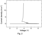
- Fig.2 presenting the current-voltage characteristics of said thyristor
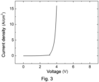
- Fig.3 presenting the current-voltage characteristics during the illumination that triggers said thyristor
- Fig.4 presenting the band structure of said thyristor.
- the embodiment of the thyristor described below contained a semiconductor layered epitaxial structure applied to the crystalline substrate 1, in which structure the first layer, counted from the aforementioned crystalline substrate 1, is the lower n-type conductivity layer 2.
- a lower undoped layer 3 a layer producing piezoelectric charges 4, an upper undoped layer 5, and an upper p-type conductivity layer 6 are present successively on the layer 2.
- Said structure was fabricated by molecular beam epitaxy on the crystalline substrate 1 made of gallium nitride with the thickness of 350 ⁇ m.
- the substrate 1 was annealed in the prechamber of the reactor at the temperature of 150°C for five hours.
- the substrate 1 was annealed for 30 minutes in the preparatory chamber at the temperature of 650°C.
- the epitaxy of the thyristor's layered structure was performed in the growth chamber in metal-rich conditions.
- the lower n-type conductivity layer 2 with the thickness of 200 nm made of gallium nitride doped with silicon in the amount of 2 ⁇ 10 18 cm -3 was applied to the substrate 1, and subsequently the lower undoped layer 3 with the thickness of 200 nm made of gallium nitride was applied.
- the growth temperature was reduced to 650°C and a layer producing piezoelectric charges 4 with the thickness of 50 nm, which was made of In 0.12 Ga 0.88 N alloy, whose band gap is 3.0 eV and is 0.4 eV lower than the band gap of gallium nitride, was applied.
- the temperature in the growth chamber was increased to 730°C and the upper undoped layer 5 with the thickness of 200 nm was fabricated of gallium nitride, and subsequently the upper p-type doped layer 6 with the thickness of 40 nm was fabricated of GaN doped with magnesium in the amount of 3 ⁇ 10 19 cm -3 .
- the layered structure (2-6) fabricated by epitaxy was subjected to photolithography and etching by the RIE (Reactive Ion Etching) method in order to form single devices and to uncover the lower n-type doped layer 2. The etching was performed to the depth of 490 nm, which was up to the level of the lower n-type doped layer 2.
- the first current terminal 7 made of Ni/Au with the thickness of 25nm/75nm was applied to the upper p-type doped layer 6 according to a known method.
- openings 9 with the shape of square with the side length of 5 ⁇ m were made in the current terminal 7 by the photolithography and RIE methods. The distances between the adjacent square openings 5 were 5 ⁇ m.
- the structure was divided into individual devices with the dimensions of 300 ⁇ 300 ⁇ 350 ⁇ m and said devices were installed in enclosures.
- the layer producing piezoelectric charges 4 can be composed of a stack of five sublayers made of an indium gallium nitride alloy and of an aluminium gallium nitride alloy, which are placed alternately.
- the first sublayer made of In 0.12 Ga 0.88 N was applied in the same manner as described above to the lower undoped layer 3.
- the second sublayer made of Al 0.06 Ga 0.94 N was applied.
- the third sublayer made of In 0.12 Ga 0.88 N was applied at the temperature of 650°C
- the fourth sublayer made of Al 0.06 Ga 0.94 N was applied at the temperature of 730°C.
- the application of the layer producing piezoelectric charges 4 was finished by the application of the fifth sublayer made of In 0.12 Ga 0.88 N at the temperature of 650°C.
- the thickness of each of the aforementioned sublayers was 20 nm.
- Subsequent layers of the epitaxial structure (5, 6) and both current terminals 7 and 8 were applied according to the aforementioned method to thus fabricated alternative layer producing piezoelectric charges 4.
- a thyristor obtained according to the above method is characterised by a high electric voltage of up to 8.3 V at low current densities. At higher current densities, the voltage decreases, which is caused by the screening of the piezoelectric charges and by the reduction of the energy barrier formed by said charges.
- Fig.3 shows that said barrier is no longer present during the illumination of the thyristor and the voltage is low already starting from low current densities.
- the illumination of the thyristor results in the thyristor opening and in a considerable current increment.
- Fig.4 presents the profile of the conduction band minimum and the profile of the valence band maximum of the thyristor with the visible energy barrier which is formed as a result of the presence of piezoelectric charges.
- a negative electric charge is present on the border between the lower undoped layer 3 and the layer producing piezoelectric charges 4, while a positive electric charge is present on the border between the layer producing piezoelectric charges 4 and the upper undoped layer 5.
- These charges are formed because a material which is characterised by a high piezoelectric coefficient and by a lattice misfit with the substrate was used as the layer producing piezoelectric charges 4.
- the negative charge present on the border between the layers 3 and 4 causes the formation of a potential barrier for the electron flow in the direction from terminal 8 to terminal 7.
- the positive charge present on the border between the layers 4 and 5 causes the formation of a potential barrier for the hole flow in the direction from terminal 7 to terminal 8.
- the illumination of the thyristor with light through the openings 9 in the terminal 7, with an energy above the value of the band gap of the material applied as the layer producing piezoelectric charges 4 causes the formation of electron-hole pairs inside the layer producing piezoelectric charges 4.
- the electron-hole pairs are separated as a result of the built-in electric field, the electrons are aggregated in the vicinity of the positive charge on the border between the layers 4 and 5, while the holes are aggregated in the vicinity of the negative charge on the border between the layers 3 and 4.
- the aggregation of the electrons and the holes leads to the screening of the charges on the borders between the layers 4 and 5 and on the borders between the layers 3 and 4, respectively.
- the screening of said charges leads to the elimination of the potential barriers and to the free electron flow in the direction from the terminal 8 to the terminal 7 and to the hole flow in the direction from the terminal 7 to the terminal 8.
- Such a structure enables the control of the current flow with the use of light.
Landscapes
- Physical Deposition Of Substances That Are Components Of Semiconductor Devices (AREA)
- Thyristors (AREA)
Applications Claiming Priority (1)
| Application Number | Priority Date | Filing Date | Title |
|---|---|---|---|
| PL442428A PL442428A1 (pl) | 2022-09-30 | 2022-09-30 | Tyrystor przełączany światłem i sposób wytwarzania takiego tyrystora |
Publications (1)
| Publication Number | Publication Date |
|---|---|
| EP4345919A1 true EP4345919A1 (de) | 2024-04-03 |
Family
ID=88511497
Family Applications (1)
| Application Number | Title | Priority Date | Filing Date |
|---|---|---|---|
| EP23199813.9A Pending EP4345919A1 (de) | 2022-09-30 | 2023-09-26 | Lichtzündbarer thyristor und verfahren zu seiner herstellung |
Country Status (2)
| Country | Link |
|---|---|
| EP (1) | EP4345919A1 (de) |
| PL (1) | PL442428A1 (de) |
Citations (6)
| Publication number | Priority date | Publication date | Assignee | Title |
|---|---|---|---|---|
| US2655610A (en) | 1952-07-22 | 1953-10-13 | Bell Telephone Labor Inc | Semiconductor signal translating device |
| US4806997A (en) | 1985-06-14 | 1989-02-21 | AT&T Laboratories American Telephone and Telegraph Company | Double heterostructure optoelectronic switch |
| US4829357A (en) | 1986-12-22 | 1989-05-09 | Nec Corporation | PNPN thyristor |
| US5539217A (en) | 1993-08-09 | 1996-07-23 | Cree Research, Inc. | Silicon carbide thyristor |
| JP2001135854A (ja) * | 1999-11-05 | 2001-05-18 | Toyoda Gosei Co Ltd | Iii族窒化物系化合物半導体素子 |
| JP2017152542A (ja) * | 2016-02-24 | 2017-08-31 | ユニークチップス合同会社 | 光駆動半導体素子 |
Family Cites Families (2)
| Publication number | Priority date | Publication date | Assignee | Title |
|---|---|---|---|---|
| WO2004061923A1 (en) * | 2002-12-27 | 2004-07-22 | General Electric Company | Gallium nitride crystal, homoepitaxial gallium-nitride-based devices and method for producing same |
| US8729559B2 (en) * | 2010-10-13 | 2014-05-20 | Soraa, Inc. | Method of making bulk InGaN substrates and devices thereon |
-
2022
- 2022-09-30 PL PL442428A patent/PL442428A1/pl unknown
-
2023
- 2023-09-26 EP EP23199813.9A patent/EP4345919A1/de active Pending
Patent Citations (6)
| Publication number | Priority date | Publication date | Assignee | Title |
|---|---|---|---|---|
| US2655610A (en) | 1952-07-22 | 1953-10-13 | Bell Telephone Labor Inc | Semiconductor signal translating device |
| US4806997A (en) | 1985-06-14 | 1989-02-21 | AT&T Laboratories American Telephone and Telegraph Company | Double heterostructure optoelectronic switch |
| US4829357A (en) | 1986-12-22 | 1989-05-09 | Nec Corporation | PNPN thyristor |
| US5539217A (en) | 1993-08-09 | 1996-07-23 | Cree Research, Inc. | Silicon carbide thyristor |
| JP2001135854A (ja) * | 1999-11-05 | 2001-05-18 | Toyoda Gosei Co Ltd | Iii族窒化物系化合物半導体素子 |
| JP2017152542A (ja) * | 2016-02-24 | 2017-08-31 | ユニークチップス合同会社 | 光駆動半導体素子 |
Non-Patent Citations (7)
| Title |
|---|
| JOURNAL OF ALLOYS AND COMPOUNDS, vol. 747, 2018, pages 354 |
| JOURNAL OF CRYSTAL GROWTH, vol. 145, 1994, pages 214 |
| JPN. J. APPL. PHYS., vol. 31, 1992, pages L139 |
| JPN. J.APPL. PHYS., vol. 42, 2003, pages 50 |
| M TRIVEDI ET AL., JOURNAL OF APPLIED PHYSICS, vol. 88, 2000, pages 7313 |
| NAKAJIMA AKIRA ET AL: "High Density Two-Dimensional Hole Gas Induced by Negative Polarization at GaN/AlGaN Heterointerface", APPLIED PHYSICS EXPRESS, vol. 3, no. 12, 10 December 2010 (2010-12-10), JP, pages 121004, XP093132415, ISSN: 1882-0778, DOI: 10.1143/APEX.3.121004 * |
| Z.Z. BANDIC ET AL., SOLID-STATE ELECTRONICS, vol. 44, 2000, pages 221 |
Also Published As
| Publication number | Publication date |
|---|---|
| PL442428A1 (pl) | 2024-04-02 |
Similar Documents
| Publication | Publication Date | Title |
|---|---|---|
| JP5011069B2 (ja) | 小さな寄生抵抗を有する低電圧ダイオードおよび製造方法 | |
| US8288798B2 (en) | Step doping in extensions of III-V family semiconductor devices | |
| US9293561B2 (en) | High voltage III-nitride semiconductor devices | |
| EP2737537B1 (de) | Halbleiter-feldeffekttransistor mit einem gruppe-iii-nitrid-metallisolator | |
| JP4660733B2 (ja) | 縦型デバイスのための裏面オーミックコンタクトの低温形成 | |
| JP5334149B2 (ja) | 窒化物半導体電界効果トランジスタ | |
| CN111509041B (zh) | 半导体器件及其制造方法 | |
| US11769825B2 (en) | Nitride semiconductor device and nitride semiconductor package | |
| US8309988B2 (en) | Field effect transistor | |
| US7037817B2 (en) | Semiconductor device and method for fabricating the same | |
| KR20060050558A (ko) | 반도체 기판 및 반도체 기판 상에 에피택셜 성장에 의해제조된 반도체 장치 | |
| JP2007519231A (ja) | Iii族窒化物素子の不動態化およびその方法 | |
| US10177239B2 (en) | HEMT transistor | |
| US8853063B2 (en) | Method and system for carbon doping control in gallium nitride based devices | |
| JP5510324B2 (ja) | 電界効果トランジスタの製造方法 | |
| JP2019012827A (ja) | 窒化ガリウム系の半導体装置及びその製造方法 | |
| US6342411B1 (en) | Electronic component and method for manufacture | |
| CN115621310B (zh) | 半导体装置以及其制作方法 | |
| EP4345919A1 (de) | Lichtzündbarer thyristor und verfahren zu seiner herstellung | |
| CN114141870A (zh) | 一种可靠性增强的iii族氮化物半导体高电子迁移率晶体管及其制造方法 | |
| JP2018093239A (ja) | 半導体装置 | |
| CN116845093A (zh) | 半导体结构及其制备方法、半导体器件及半导体晶圆 | |
| US11973137B2 (en) | Stacked buffer in transistors | |
| EP4723168A1 (de) | Halbleiteranordnung | |
| EP4560695A1 (de) | Hemt mit diffusionssperrschicht |
Legal Events
| Date | Code | Title | Description |
|---|---|---|---|
| PUAI | Public reference made under article 153(3) epc to a published international application that has entered the european phase |
Free format text: ORIGINAL CODE: 0009012 |
|
| STAA | Information on the status of an ep patent application or granted ep patent |
Free format text: STATUS: THE APPLICATION HAS BEEN PUBLISHED |
|
| AK | Designated contracting states |
Kind code of ref document: A1 Designated state(s): AL AT BE BG CH CY CZ DE DK EE ES FI FR GB GR HR HU IE IS IT LI LT LU LV MC ME MK MT NL NO PL PT RO RS SE SI SK SM TR |
|
| STAA | Information on the status of an ep patent application or granted ep patent |
Free format text: STATUS: REQUEST FOR EXAMINATION WAS MADE |
|
| 17P | Request for examination filed |
Effective date: 20240920 |
|
| RBV | Designated contracting states (corrected) |
Designated state(s): AL AT BE BG CH CY CZ DE DK EE ES FI FR GB GR HR HU IE IS IT LI LT LU LV MC ME MK MT NL NO PL PT RO RS SE SI SK SM TR |