EP4350313A1 - Film de résistance à la contrainte, capteur de quantité physique et procédé de fabrication du film de résistance à la contrainte - Google Patents
Film de résistance à la contrainte, capteur de quantité physique et procédé de fabrication du film de résistance à la contrainte Download PDFInfo
- Publication number
- EP4350313A1 EP4350313A1 EP23201170.0A EP23201170A EP4350313A1 EP 4350313 A1 EP4350313 A1 EP 4350313A1 EP 23201170 A EP23201170 A EP 23201170A EP 4350313 A1 EP4350313 A1 EP 4350313A1
- Authority
- EP
- European Patent Office
- Prior art keywords
- resistance film
- strain resistance
- film
- strain
- factor
- Prior art date
- Legal status (The legal status is an assumption and is not a legal conclusion. Google has not performed a legal analysis and makes no representation as to the accuracy of the status listed.)
- Pending
Links
Images


Classifications
-
- C—CHEMISTRY; METALLURGY
- C23—COATING METALLIC MATERIAL; COATING MATERIAL WITH METALLIC MATERIAL; CHEMICAL SURFACE TREATMENT; DIFFUSION TREATMENT OF METALLIC MATERIAL; COATING BY VACUUM EVAPORATION, BY SPUTTERING, BY ION IMPLANTATION OR BY CHEMICAL VAPOUR DEPOSITION, IN GENERAL; INHIBITING CORROSION OF METALLIC MATERIAL OR INCRUSTATION IN GENERAL
- C23C—COATING METALLIC MATERIAL; COATING MATERIAL WITH METALLIC MATERIAL; SURFACE TREATMENT OF METALLIC MATERIAL BY DIFFUSION INTO THE SURFACE, BY CHEMICAL CONVERSION OR SUBSTITUTION; COATING BY VACUUM EVAPORATION, BY SPUTTERING, BY ION IMPLANTATION OR BY CHEMICAL VAPOUR DEPOSITION, IN GENERAL
- C23C14/00—Coating by vacuum evaporation, by sputtering or by ion implantation of the coating forming material
- C23C14/06—Coating by vacuum evaporation, by sputtering or by ion implantation of the coating forming material characterised by the coating material
- C23C14/0676—Oxynitrides
-
- C—CHEMISTRY; METALLURGY
- C22—METALLURGY; FERROUS OR NON-FERROUS ALLOYS; TREATMENT OF ALLOYS OR NON-FERROUS METALS
- C22C—ALLOYS
- C22C27/00—Alloys based on rhenium or a refractory metal not mentioned in groups C22C14/00 or C22C16/00
- C22C27/06—Alloys based on chromium
-
- G—PHYSICS
- G01—MEASURING; TESTING
- G01L—MEASURING FORCE, STRESS, TORQUE, WORK, MECHANICAL POWER, MECHANICAL EFFICIENCY, OR FLUID PRESSURE
- G01L1/00—Measuring force or stress, in general
- G01L1/20—Measuring force or stress, in general by measuring variations in ohmic resistance of solid materials or of electrically-conductive fluids; by making use of electrokinetic cells, i.e. liquid-containing cells wherein an electrical potential is produced or varied upon the application of stress
- G01L1/22—Measuring force or stress, in general by measuring variations in ohmic resistance of solid materials or of electrically-conductive fluids; by making use of electrokinetic cells, i.e. liquid-containing cells wherein an electrical potential is produced or varied upon the application of stress using resistance strain gauges
- G01L1/2287—Measuring force or stress, in general by measuring variations in ohmic resistance of solid materials or of electrically-conductive fluids; by making use of electrokinetic cells, i.e. liquid-containing cells wherein an electrical potential is produced or varied upon the application of stress using resistance strain gauges constructional details of the strain gauges
- G01L1/2293—Measuring force or stress, in general by measuring variations in ohmic resistance of solid materials or of electrically-conductive fluids; by making use of electrokinetic cells, i.e. liquid-containing cells wherein an electrical potential is produced or varied upon the application of stress using resistance strain gauges constructional details of the strain gauges of the semi-conductor type
-
- C—CHEMISTRY; METALLURGY
- C23—COATING METALLIC MATERIAL; COATING MATERIAL WITH METALLIC MATERIAL; CHEMICAL SURFACE TREATMENT; DIFFUSION TREATMENT OF METALLIC MATERIAL; COATING BY VACUUM EVAPORATION, BY SPUTTERING, BY ION IMPLANTATION OR BY CHEMICAL VAPOUR DEPOSITION, IN GENERAL; INHIBITING CORROSION OF METALLIC MATERIAL OR INCRUSTATION IN GENERAL
- C23C—COATING METALLIC MATERIAL; COATING MATERIAL WITH METALLIC MATERIAL; SURFACE TREATMENT OF METALLIC MATERIAL BY DIFFUSION INTO THE SURFACE, BY CHEMICAL CONVERSION OR SUBSTITUTION; COATING BY VACUUM EVAPORATION, BY SPUTTERING, BY ION IMPLANTATION OR BY CHEMICAL VAPOUR DEPOSITION, IN GENERAL
- C23C14/00—Coating by vacuum evaporation, by sputtering or by ion implantation of the coating forming material
- C23C14/0021—Reactive sputtering or evaporation
- C23C14/0036—Reactive sputtering
- C23C14/0042—Controlling partial pressure or flow rate of reactive or inert gases with feedback of measurements
-
- C—CHEMISTRY; METALLURGY
- C23—COATING METALLIC MATERIAL; COATING MATERIAL WITH METALLIC MATERIAL; CHEMICAL SURFACE TREATMENT; DIFFUSION TREATMENT OF METALLIC MATERIAL; COATING BY VACUUM EVAPORATION, BY SPUTTERING, BY ION IMPLANTATION OR BY CHEMICAL VAPOUR DEPOSITION, IN GENERAL; INHIBITING CORROSION OF METALLIC MATERIAL OR INCRUSTATION IN GENERAL
- C23C—COATING METALLIC MATERIAL; COATING MATERIAL WITH METALLIC MATERIAL; SURFACE TREATMENT OF METALLIC MATERIAL BY DIFFUSION INTO THE SURFACE, BY CHEMICAL CONVERSION OR SUBSTITUTION; COATING BY VACUUM EVAPORATION, BY SPUTTERING, BY ION IMPLANTATION OR BY CHEMICAL VAPOUR DEPOSITION, IN GENERAL
- C23C14/00—Coating by vacuum evaporation, by sputtering or by ion implantation of the coating forming material
- C23C14/22—Coating by vacuum evaporation, by sputtering or by ion implantation of the coating forming material characterised by the process of coating
- C23C14/24—Vacuum evaporation
-
- C—CHEMISTRY; METALLURGY
- C23—COATING METALLIC MATERIAL; COATING MATERIAL WITH METALLIC MATERIAL; CHEMICAL SURFACE TREATMENT; DIFFUSION TREATMENT OF METALLIC MATERIAL; COATING BY VACUUM EVAPORATION, BY SPUTTERING, BY ION IMPLANTATION OR BY CHEMICAL VAPOUR DEPOSITION, IN GENERAL; INHIBITING CORROSION OF METALLIC MATERIAL OR INCRUSTATION IN GENERAL
- C23C—COATING METALLIC MATERIAL; COATING MATERIAL WITH METALLIC MATERIAL; SURFACE TREATMENT OF METALLIC MATERIAL BY DIFFUSION INTO THE SURFACE, BY CHEMICAL CONVERSION OR SUBSTITUTION; COATING BY VACUUM EVAPORATION, BY SPUTTERING, BY ION IMPLANTATION OR BY CHEMICAL VAPOUR DEPOSITION, IN GENERAL
- C23C14/00—Coating by vacuum evaporation, by sputtering or by ion implantation of the coating forming material
- C23C14/22—Coating by vacuum evaporation, by sputtering or by ion implantation of the coating forming material characterised by the process of coating
- C23C14/34—Sputtering
- C23C14/3407—Cathode assembly for sputtering apparatus, e.g. Target
- C23C14/3414—Metallurgical or chemical aspects of target preparation, e.g. casting, powder metallurgy
-
- C—CHEMISTRY; METALLURGY
- C23—COATING METALLIC MATERIAL; COATING MATERIAL WITH METALLIC MATERIAL; CHEMICAL SURFACE TREATMENT; DIFFUSION TREATMENT OF METALLIC MATERIAL; COATING BY VACUUM EVAPORATION, BY SPUTTERING, BY ION IMPLANTATION OR BY CHEMICAL VAPOUR DEPOSITION, IN GENERAL; INHIBITING CORROSION OF METALLIC MATERIAL OR INCRUSTATION IN GENERAL
- C23C—COATING METALLIC MATERIAL; COATING MATERIAL WITH METALLIC MATERIAL; SURFACE TREATMENT OF METALLIC MATERIAL BY DIFFUSION INTO THE SURFACE, BY CHEMICAL CONVERSION OR SUBSTITUTION; COATING BY VACUUM EVAPORATION, BY SPUTTERING, BY ION IMPLANTATION OR BY CHEMICAL VAPOUR DEPOSITION, IN GENERAL
- C23C14/00—Coating by vacuum evaporation, by sputtering or by ion implantation of the coating forming material
- C23C14/22—Coating by vacuum evaporation, by sputtering or by ion implantation of the coating forming material characterised by the process of coating
- C23C14/34—Sputtering
- C23C14/3464—Sputtering using more than one target
-
- C—CHEMISTRY; METALLURGY
- C23—COATING METALLIC MATERIAL; COATING MATERIAL WITH METALLIC MATERIAL; CHEMICAL SURFACE TREATMENT; DIFFUSION TREATMENT OF METALLIC MATERIAL; COATING BY VACUUM EVAPORATION, BY SPUTTERING, BY ION IMPLANTATION OR BY CHEMICAL VAPOUR DEPOSITION, IN GENERAL; INHIBITING CORROSION OF METALLIC MATERIAL OR INCRUSTATION IN GENERAL
- C23C—COATING METALLIC MATERIAL; COATING MATERIAL WITH METALLIC MATERIAL; SURFACE TREATMENT OF METALLIC MATERIAL BY DIFFUSION INTO THE SURFACE, BY CHEMICAL CONVERSION OR SUBSTITUTION; COATING BY VACUUM EVAPORATION, BY SPUTTERING, BY ION IMPLANTATION OR BY CHEMICAL VAPOUR DEPOSITION, IN GENERAL
- C23C14/00—Coating by vacuum evaporation, by sputtering or by ion implantation of the coating forming material
- C23C14/22—Coating by vacuum evaporation, by sputtering or by ion implantation of the coating forming material characterised by the process of coating
- C23C14/34—Sputtering
- C23C14/3492—Variation of parameters during sputtering
-
- C—CHEMISTRY; METALLURGY
- C23—COATING METALLIC MATERIAL; COATING MATERIAL WITH METALLIC MATERIAL; CHEMICAL SURFACE TREATMENT; DIFFUSION TREATMENT OF METALLIC MATERIAL; COATING BY VACUUM EVAPORATION, BY SPUTTERING, BY ION IMPLANTATION OR BY CHEMICAL VAPOUR DEPOSITION, IN GENERAL; INHIBITING CORROSION OF METALLIC MATERIAL OR INCRUSTATION IN GENERAL
- C23C—COATING METALLIC MATERIAL; COATING MATERIAL WITH METALLIC MATERIAL; SURFACE TREATMENT OF METALLIC MATERIAL BY DIFFUSION INTO THE SURFACE, BY CHEMICAL CONVERSION OR SUBSTITUTION; COATING BY VACUUM EVAPORATION, BY SPUTTERING, BY ION IMPLANTATION OR BY CHEMICAL VAPOUR DEPOSITION, IN GENERAL
- C23C14/00—Coating by vacuum evaporation, by sputtering or by ion implantation of the coating forming material
- C23C14/22—Coating by vacuum evaporation, by sputtering or by ion implantation of the coating forming material characterised by the process of coating
- C23C14/54—Controlling or regulating the coating process
- C23C14/548—Controlling the composition
-
- C—CHEMISTRY; METALLURGY
- C23—COATING METALLIC MATERIAL; COATING MATERIAL WITH METALLIC MATERIAL; CHEMICAL SURFACE TREATMENT; DIFFUSION TREATMENT OF METALLIC MATERIAL; COATING BY VACUUM EVAPORATION, BY SPUTTERING, BY ION IMPLANTATION OR BY CHEMICAL VAPOUR DEPOSITION, IN GENERAL; INHIBITING CORROSION OF METALLIC MATERIAL OR INCRUSTATION IN GENERAL
- C23C—COATING METALLIC MATERIAL; COATING MATERIAL WITH METALLIC MATERIAL; SURFACE TREATMENT OF METALLIC MATERIAL BY DIFFUSION INTO THE SURFACE, BY CHEMICAL CONVERSION OR SUBSTITUTION; COATING BY VACUUM EVAPORATION, BY SPUTTERING, BY ION IMPLANTATION OR BY CHEMICAL VAPOUR DEPOSITION, IN GENERAL
- C23C14/00—Coating by vacuum evaporation, by sputtering or by ion implantation of the coating forming material
- C23C14/58—After-treatment
- C23C14/5806—Thermal treatment
-
- G—PHYSICS
- G01—MEASURING; TESTING
- G01B—MEASURING LENGTH, THICKNESS OR SIMILAR LINEAR DIMENSIONS; MEASURING ANGLES; MEASURING AREAS; MEASURING IRREGULARITIES OF SURFACES OR CONTOURS
- G01B7/00—Measuring arrangements characterised by the use of electric or magnetic techniques
- G01B7/16—Measuring arrangements characterised by the use of electric or magnetic techniques for measuring the deformation in a solid, e.g. by resistance strain gauge
- G01B7/18—Measuring arrangements characterised by the use of electric or magnetic techniques for measuring the deformation in a solid, e.g. by resistance strain gauge using change in resistance
-
- G—PHYSICS
- G01—MEASURING; TESTING
- G01L—MEASURING FORCE, STRESS, TORQUE, WORK, MECHANICAL POWER, MECHANICAL EFFICIENCY, OR FLUID PRESSURE
- G01L9/00—Measuring steady of quasi-steady pressure of fluid or fluent solid material by electric or magnetic pressure-sensitive elements; Transmitting or indicating the displacement of mechanical pressure-sensitive elements, used to measure the steady or quasi-steady pressure of a fluid or fluent solid material, by electric or magnetic means
- G01L9/0041—Transmitting or indicating the displacement of flexible diaphragms
- G01L9/0051—Transmitting or indicating the displacement of flexible diaphragms using variations in ohmic resistance
-
- H—ELECTRICITY
- H01—ELECTRIC ELEMENTS
- H01C—RESISTORS
- H01C17/00—Apparatus or processes specially adapted for manufacturing resistors
- H01C17/06—Apparatus or processes specially adapted for manufacturing resistors adapted for coating resistive material on a base
- H01C17/065—Apparatus or processes specially adapted for manufacturing resistors adapted for coating resistive material on a base by thick film techniques, e.g. serigraphy
- H01C17/06506—Precursor compositions therefor, e.g. pastes, inks, glass frits or green body
- H01C17/06513—Precursor compositions therefor, e.g. pastes, inks, glass frits or green body characterised by the resistive component
- H01C17/06533—Precursor compositions therefor, e.g. pastes, inks, glass frits or green body characterised by the resistive component composed of oxides
-
- H—ELECTRICITY
- H01—ELECTRIC ELEMENTS
- H01C—RESISTORS
- H01C7/00—Non-adjustable resistors formed as one or more layers or coatings; Non-adjustable resistors made from powdered conducting material or powdered semi-conducting material with or without insulating material
- H01C7/06—Non-adjustable resistors formed as one or more layers or coatings; Non-adjustable resistors made from powdered conducting material or powdered semi-conducting material with or without insulating material including means to minimise changes in resistance with changes in temperature
-
- H—ELECTRICITY
- H01—ELECTRIC ELEMENTS
- H01C—RESISTORS
- H01C17/00—Apparatus or processes specially adapted for manufacturing resistors
- H01C17/06—Apparatus or processes specially adapted for manufacturing resistors adapted for coating resistive material on a base
- H01C17/075—Apparatus or processes specially adapted for manufacturing resistors adapted for coating resistive material on a base by thin-film techniques
Definitions
- the disclosure relates to a strain resistance film in which resistance value changes according to strain, and a physical quantity sensor using thereof.
- CrAl film or CrAlN film is a material that exhibits a high k-factor up to high temperatures, and is noted as a detection material for pressure sensors and strain sensors that can with stand high temperatures.
- Patent Document 1 describes an example thereof.
- the conductive properties change from metal to semiconductor at a certain Al content ratio. It becomes possible to control the temperature coefficient of resistance (TCR) by controlling this conduction property.
- TCR temperature coefficient of resistance
- TCR which is one of the above conductive properties, has been controlled by the annealing temperature at the same Cr-Al ratio. Also, k-factor is controlled by changing Cr-Al composition ratio and the annealing temperature. Therefore, when adjusting TCR for each product, it was necessary to adjust Cr-Al composition ratio of the material for each product.
- Patent Document 1 Japanese unexamined patent publication 2018-91848
- the strain resistance film has a composition represented by Cr 100-x-y-z Al x N y O z which satisfies 5 ⁇ x ⁇ 50, 0.1 ⁇ y ⁇ 20, 0.1 ⁇ z ⁇ 17, and y+z ⁇ 25.
- the physical quantity sensor has the strain resistance film described above.
- the physical quantity sensor is not particularly limited, and examples thereof include such as strain sensors and pressure sensors.
- a manufacturing method for a strain resistance film is
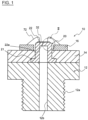
- FIG. 1 is a schematic cross-sectional view of pressure sensor 10 using a strain resistance film 32 according to an embodiment.
- the pressure sensor 10 has a membrane 22 that deforms in response to pressure.
- the membrane 22 is configured with an end wall formed at one end of a hollow cylindrical stem 20, however, it can also be configured with a flat Si substrate 122 (See Fig. 3B ) as in Example.
- the other end of the stem 20 is an open end of a hollow, and the hollow of the stem 20 communicates with the flow path 12b of the connecting member 12.
- the fluid introduced into the flow path 12b is guided from the hollow of the stem 20 to the inner surface 22a of the membrane 22 to apply fluid pressure to the membrane 22.
- Stem 20 is composed of metal such as stainless steel.
- the shape corresponding to the stem 20 may be formed by etching a silicon substrate or bonding the flat silicon substrate to another member.
- a flange 21 is formed around the open end of the stem 20 so as to protrude outward from the axis of the stem 20.
- the flange 21 is between the connecting member 12 and the suppressing member 14 so that the channel 12b leading to the inner surface 22a of the membrane 22 is sealed.
- the connecting member 12 has a thread groove 12a for fixing the pressure sensor 10.
- the pressure sensor 10 is fixed via the thread groove 12a to a pressure chamber or the like in which a fluid to be measured is enclosed.
- the channel 12b formed inside the connecting member12 and the inner surface 22a of the membrane 22 of the stem 20 are airtightly communicated with the pressure chamber in which the fluid to be measured exists.
- a circuit board 16 is attached to the upper surface of the suppressing member 14.
- the circuit board 16 has a ring shape surrounding the stem 20, but the shape of the circuit board 16 is not limited thereto.
- the circuit board 16 incorporates, for example, a circuit to which the detection signal from the strain resistance film 32 is transmitted.
- a strain resistance film 32 and the like are provided on the outer surface of the membrane 22.
- the strain resistance film 32 and the circuit board 16 are electrically connected via an intermediate wiring 72 or the like by wire bonding or the like.
- FIG. 2 is a schematic cross-sectional view showing an enlarged view of a part of the strain resistance film 32 included in the pressure sensor 10 shown in FIG. 1 and its surroundings.
- the strain resistance film 32 is provided on the outer surface 22b of the membrane 22 via the base insulating layer 52 or the like.
- the base insulating layer 52 is formed to cover substantially the entire outer surface 22b of the membrane 22, and is made of silicon oxide such as SiO 2 , silicon nitride, or silicon oxynitride and the like.
- the thickness of the base insulating layer 52 is preferably 10 ⁇ m or less, more preferably 1 to 5 ⁇ m.
- the base insulating layer 52 can be formed on the outer surface 22b of the membrane 22 by a vapor deposition of CVD and the like.
- the strain resistance film 32 may be formed directly on the outer surface 22b of the membrane 22 without forming the base insulating layer 52.
- the membrane 22 is made of an insulating material such as alumina, the strain resistance film 32 may be provided directly on the membrane 22.
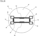
- FIG. 3A is a schematic plan view of the strain resistance film 30 with electrodes shown in FIGS. 1 and 2 as viewed from above, and shows the pattern arrangement of the strain resistance film 30 with electrodes.
- the strain resistance film 32 has a first resistor R1, a second resistor R2, a third resistor R3 and a fourth resistor R4 formed in a predetermined pattern.
- the first to fourth resistors R1, R2, R3, and R4 generate strain according to the deformation of the membrane 22, and the resistance value changes according to the deformation of the membrane 22.
- These first to fourth resistors R1 to R4 are connected by electrical wiring 34 so as to form a Wheatstone bridge circuit.
- the pressure sensor 10 shown in FIG. 1 detects the fluid pressure acting on the membrane 22 from the output of the Wheatstone bridge circuit by the first to fourth resistors R1 to R4 shown in FIG. 3A . That is, the first to fourth resistors R1 to R4 are provided at positions where the membrane 22 shown in FIGS. 1 and 2 is deformed and strained by the fluid pressure, and the resistance value changes according to the amount of strain.
- the strain resistance film 32 having the first to fourth resistors R1 to R4 can be manufactured by such as patterning a conductive thin film of a predetermined material.
- the strain resistance film 32 has a composition represented by the composition Cr 100-x-y-z Al x N y O z where 5 ⁇ x ⁇ 50, 0.1 ⁇ y ⁇ 20, 0.1 ⁇ z ⁇ 17 which satisfies y+z ⁇ 25.
- the lower limit of "x” may be preferably 12.7 or more, 23 or more, or 25 or more.
- the upper limit of “x” may be 40 or less, or 30 or less.
- "y” is preferably 1.1 to 12.2.
- "z” may be preferably 0.4 to 1.3, more preferably 0.4 to 0.7 or 2.6 to 9.5.
- "y+z” may be preferably 12.0 to 19.6, more preferably 14.0 to 19.6, or 1.8 to 10.7.
- the thickness of the strain resistance film 32 is not particularly limited, it is preferably one nm or more, more preferably 10 nm or more. Although upper limit of the thickness is not particularly limited, it may be 1000nm or less or 500nm or less.
- An oxide film or the like may be formed on the surface of the strain resistance film 32.
- the oxide film include a chromium oxide film, a silicon oxide film, a silicon nitride film, a silicon oxynitride film, an aluminum oxide film, an aluminum nitride film, an aluminum oxynitride film, and the like.
- composition analysis of "x", “y”, “z”, etc. in the strain resistance film 32 may be performed using XRF (X-ray fluorescence) method, XPS (X-ray photoelectron spectroscopy), etc.
- XRF X-ray fluorescence
- XPS X-ray photoelectron spectroscopy
- the strain resistance film 32 may contain trace amounts of metals and nonmetallic elements other than Cr and Al.
- metal and non-metal elements other than Cr and Al contained in the strain resistance film 32 include Ti, Nb, Ta, Ni, Zr, Hf, Si, Ge, C, P, Se, Te, Zn, Cu, Bi, Fe, Mo, W, As, Sn, Sb, Pb, B, Ge, In, Tl, Ru, Rh, Re, Os, Ir, Pt, Pd, Ag, Au, Co, Be, Mg, Ca, Sr, Ba, Mn and rare earth elements are included.
- the strain resistance film 32 can be formed by a thin film method such as sputtering or vapor deposition.
- the first to fourth resistors R1 to R4 shown in FIG. 3A can be formed by such as patterning a thin film into a meandering shape.
- the electrical wiring 34, as shown in FIG. 3A may be formed by patterning the strain resistance film 32 or by a conductive film or layer different from the strain resistance film 32.
- strain resistance film 32 is preferably intentionally introduced into the strain resistance film 32 by being used as an atmosphere gas during film formation of the strain resistance film, however, may be intentionally introduced into the strain resistance film 32 by used as atmosphere gases for annealing. Alternatively, it may be a substance that was not completely removed from the reaction chamber when the strain resistance film 32 was formed, and was taken into the strain resistance film 32.
- k-factor and TCR Temporal Coefficient of Resistance
- TCR Temporal Coefficient of Resistance
- TCS Temporal Coefficient of Sensitivity
- the conditions in the sputtering apparatus are preferably 0.08 to 0.2 Pa, and the atmosphere gas for manufacturing contains an inert gas, nitrogen gas and oxygen gas.
- the partial pressure of nitrogen gas is preferably 0 to 20%
- the partial pressure of oxygen gas is preferably 0 to 15%
- the rest is the partial pressure of inert gas.
- Ar gas, Ne gas, or the like can be used as the inert gas.
- the strain resistance film 32 may be heat treated.
- the heat treatment temperature is not particularly limited, it may be such as 50°C to 550°C, preferably 350°C to 550°C.
- the electrode 36 is provided on top of the electrical wiring 34 made of the same material as the strain resistance film 32, and electrically connected to the strain resistance film 32. As shown in FIG. 2 , the electrode 36 is formed on a part of the upper surface of the electrical wiring 34 made of the strain resistance film 32. The output of the Wheatstone bridge circuit of strain resistance film 32 is transmitted to circuit board 16 shown in FIG. 1 via the electrode 36 and an intermediate wiring 72.
- the materials of the electrode 36 include conductive metals, alloys, and the like, and more specifically, Cr, Ti, Ni, Mo, platinum group elements, Au, and the like. Further, the electrode 36 may have a multi-layer structure made of different materials.
- the base insulating layer 52 and the electrode 36 shown in FIG. 2 can also be formed by a thin film method such as sputtering or vapor deposition, similarly to the strain resistance film 32, however, the base insulating layer 52 and the electrode 36 may be formed by a method other than the thin film method.
- the base insulating layer 52 of SiO 2 film may be provided on the surface of the Si substrate by heating the Si substrate surface and forming a thermal oxide film.
- the TCR can be easily controlled while maintaining a high k-factor of four or more.
- the k-factor corresponds to the gauge factor of the pressure sensor.
- TCR temperature resistance coefficient
- the strain resistance film that satisfies the above composition ratio is possible to maintain a high k-factor of four or more, while making an absolute value of the temperature coefficient of sensitivity (TCS) to preferably 2000 ppm/°C or less, more preferably 1000 ppm/°C or less in the temperature range of -50°C or more to 450°C or less.
- TCS temperature coefficient of sensitivity
- Such strain resistance film 32 has a small resistance value change (and/or sensitivity change) accompanying temperature change over a wide range from low temperature to high temperature.
- the strain resistance film 32 is preferably used as the strain resistance film 32 of the pressure sensor 10 used in a wide temperature range, and can reduce temperature correction error and perform highly accurate detection.
- the strain resistance film 32 of the embodiment In order to manufacture the strain resistance film 32 of the embodiment, a target having a fixed ratio of Cr and Al is used, and by such as controlling the amounts of nitrogen and oxygen in the atmosphere gas used for manufacturing the film, the nitrogen and/or oxygen contents in the obtained resistance film can be controlled and the k-factor and TCR of the strain resistance film can be controlled.
- the strain resistance film 32 satisfying the above composition ratio, it is easy to control the resistivity ( ⁇ ) of the strain resistance film 32 to 1 to 15 ⁇ m.
- ⁇ resistivity
- a circuit for sensor such as a Wheatstone bridge circuit can be easily manufactured using the strained resistance film 32.
- the strain resistance film 32 has a film thickness of 10 nm or more.
- the k-factor and TCR of the strain resistance film 32 can be easily controlled.
- the manufacturing method of the strain resistance film 32 of the embodiment for example, by using a target having a fixed ratio of Cr and Al and controlling the amount of nitrogen and/or oxygen in the atmosphere gas for manufacturing the film, the nitrogen and the oxygen contents in the obtained strain resistance film can be controlled and the k-factor and TCR (and/or TCS) of the strain resistance film can also be controlled.
- the pressure sensor 10 is not limited to the sensor having the stem 20 shown in FIG. 1 .
- the pressure sensor 10 may be a pressure sensor manufactured by etching the substrate, or may be a sensor manufactured by bonding a flat substrate, on which a strain resistance film is formed, to the other member.
- the materials of the substrate may be any of metal, semiconductor, and insulator, and specifically, alumina (Al 2 O 3 ) and the like can be used in addition to Si mentioned in the examples.
- strain resistance film of the embodiment can be used as a physical quantity sensor other than the pressure sensor 10.
- Other physical quantity sensors include such as strain sensors, angle sensors, movement amount sensors, and acceleration sensors.
- the Si substrate 122 was prepared and its surface was heated to form the SiO 2 film 152 as a thermal oxide film on the surface of the Si substrate 122.
- the strain resistance film 132 was formed on the surface of the SiO 2 film 152 using a DC sputtering apparatus.
- the atmosphere gas in the sputtering apparatus for manufacturing the film was Ar gas containing trace amounts of nitrogen and oxygen, and the pressure of the atmosphere gas was within the range of 0.08 to 0.2 Pa. When the total pressure of the atmosphere gas was 100%, partial pressure of nitrogen gas was 0 to 20%, partial pressure of oxygen gas was 0 to 15%, and the rest was the partial pressure of inert gas.
- Strain resistance film samples 1 to 10 with different N contents (y value) and O contents (z values) were manufactured by changing the oxygen partial pressure and/or nitrogen partial pressure in the atmosphere gas during film formation, while fixing the ratio of the Cr target and the Al target used in the sputtering apparatus. The result confirmed that the higher the oxygen partial pressure in the atmosphere gas, the greater the O content (z value) in the central position along the thickness direction of the finally obtained strain resistance film.
- the strained resistance film 132 after the film formation at 350°C was annealed, then, resistors constituting a Wheatstone bridge circuit were formed in the strained resistance film 132 by microfabrication. Finally, an electrode layer was formed on the surface of the strain resistance film 132 by electron deposition to obtain samples. The average film thickness of the strain resistance film 132 in each sample was within the range of 300 nm ⁇ 30 nm. The film thickness of the strain resistance film 132 was measured using a stylus profiler.
- the composition of the strain resistance film 132 for each sample was analyzed by the XRF (X-ray fluorescence) method. Table 1 shows the results.
- the resistance value was measured by the four-terminal measurement method at 25°C.
- the specific resistance was calculated from the measured value of the sample, and the area and the thickness of the strain resistance film samples. Results are shown in Table 1.
- TCR temperature coefficient of resistance
- the resistance value was measured while changing the environmental temperature from -50 °C to 450 °C, and the relationship between the resistance value and temperature was linearly approximated by the least squares method to obtain a slope. TCR (ppm/°C) for each sample was calculated from the slope. Reference temperature of the calculated TCR was 25°C. Results are shown in Table 1.
- the gauge factor was measured while changing the environmental temperature from -50 °C to 450 °C, and the relationship between the gauge factor and the temperature was linearly approximated by the least squares method to obtain a slope. TCS (ppm/°C) for each sample was calculated from the slope. Reference temperature of the calculated TCS was 25°C, and the measured value was determined as k-factor. Results are shown in Table 1.
- Samples 11 to 15 were prepared in the same manner as in Example 1, except for reducing the number of Al targets used in the sputtering apparatus relative to Example 1, fixing the ratio of the Cr target and the Al target, and adjusting the partial pressure of the nitrogen gas in the sputtering apparatus to reduce the nitrogen content. Then, analysis was performed to the samples in the same manner as in Example 1. Results are shown in Table 2.
- Samples 21 to 23 were prepared in the same manner as in Example 1, except the atomic % of N+O in the finally obtained strain resistance film was about the same as that of sample number 7 in Example 1, which was around 14.0 atomic %, and the partial pressures of the nitrogen gas and the oxygen gas in the sputtering apparatus were adjusted so as to change the ratio of N atomic % and O atomic %. Then, analysis was performed to the samples in the same manner as in Example 1. Results are shown in Table 3.
- the composition of the finally obtained strain resistance film was the same as that of sample number 5 in Example 1, and the sputtering time of the sputtering device was controlled so that the film thickness varies to obtain strain resistance films of different thicknesses.
- FIG. 4 , FIG. 5A, and FIG. 5B confirm that the resistivity, k-factor, TCR, and TCS can be controlled simply by changing the content ratios of "N” and “O” while using targets with a fixed ratios of "Cr” and “Al", and without a need for preparing targets with different ratios of Cr and Al.
- FIGS. 4 , 5A, and 5B was a graph obtained by sampling the data shown in Table 1.
- results from Table 1 and FIG. 4 confirm that the k-factor can be changed in the range of 2 to 8 by changing the content ratio (y + z) of N + O in the strain resistance film.
- results from Table 1 and FIG. 4 also confirm that the content ratio (y + z) of N+O in the strain resistance film is preferably 25 atomic % or less in order to make k-factor four or more, and the content ratio (y + z) of N+O in the strain resistance film is preferably 20 atomic % or less in order to make k-factor six or more.
- results from Table 1 and FIG. 5A confirm that the absolute value of TCR (and TCS) is preferably 2000 or less, more preferably 1000 or less by changing the content ratio (y+z) of N+O in the strain resistance film.
- results from Table 1 and FIG. 5B confirm that the absolute value of TCR (and TCS) is preferably 2000 or less, more preferably 1000 or less by changing the content ratio (z) of "O" in the strain resistance film.
- results from Tables 1 and 3 confirm that "x" is preferably 23 to 30, "z” is preferably 0.9 to 9.5, more preferably 2.6 to 9.5, and "y+z” is preferably 12.0 to 20.0, more preferably 14.0 to 20.0, in order to make the absolute value of TCR (and TCS) to 2000 or less, more preferably 1200 or less, and further preferably 1000 or less, while maintaining the resistivity of four ⁇ m or more and the k-factor of four or more, preferably six or more, more preferably eight or more.
- results from Table 2 confirm that "x” is preferably 12 to 14, "z” is preferably 0.4 to 0.7, and “y+z” is preferably 1.8 to 10.7, in order to maintain the resistivity to three ⁇ m or more, the k-factor to eight or more, and the absolute value of TCR (and TCS) to 2000 or less, preferably 1200 or less, and more preferably 1000 or less.
- results from Tables 1 to 3 confirm that the content ratio (y) of "N" in the strain resistance film is 0.1 to 20, preferably 1.1 to 12.2.
- the thickness of the strain resistance film was preferably 10 nm or more, more preferably 30 nm or more.
Landscapes
- Chemical & Material Sciences (AREA)
- Engineering & Computer Science (AREA)
- Organic Chemistry (AREA)
- Materials Engineering (AREA)
- Mechanical Engineering (AREA)
- Metallurgy (AREA)
- Chemical Kinetics & Catalysis (AREA)
- Physics & Mathematics (AREA)
- General Physics & Mathematics (AREA)
- Microelectronics & Electronic Packaging (AREA)
- Electromagnetism (AREA)
- Manufacturing & Machinery (AREA)
- Fluid Mechanics (AREA)
- Thermal Sciences (AREA)
- Pressure Sensors (AREA)
- Measurement Of Force In General (AREA)
- Measuring Fluid Pressure (AREA)
Applications Claiming Priority (1)
| Application Number | Priority Date | Filing Date | Title |
|---|---|---|---|
| JP2022161188A JP2024054754A (ja) | 2022-10-05 | 2022-10-05 | 歪抵抗膜および物理量センサおよび歪抵抗膜の製造方法 |
Publications (1)
| Publication Number | Publication Date |
|---|---|
| EP4350313A1 true EP4350313A1 (fr) | 2024-04-10 |
Family
ID=88237745
Family Applications (1)
| Application Number | Title | Priority Date | Filing Date |
|---|---|---|---|
| EP23201170.0A Pending EP4350313A1 (fr) | 2022-10-05 | 2023-10-02 | Film de résistance à la contrainte, capteur de quantité physique et procédé de fabrication du film de résistance à la contrainte |
Country Status (4)
| Country | Link |
|---|---|
| US (1) | US20240117474A1 (fr) |
| EP (1) | EP4350313A1 (fr) |
| JP (1) | JP2024054754A (fr) |
| CN (1) | CN117848200A (fr) |
Families Citing this family (2)
| Publication number | Priority date | Publication date | Assignee | Title |
|---|---|---|---|---|
| JP7843154B2 (ja) * | 2022-02-25 | 2026-04-09 | Tdk株式会社 | 絶縁膜付き金属部材および物理量センサ |
| CN119618434B (zh) * | 2025-02-17 | 2026-02-27 | 松诺盟科技有限公司 | 齐平膜芯体及其制备方法和应用、压力变送器 |
Citations (2)
| Publication number | Priority date | Publication date | Assignee | Title |
|---|---|---|---|---|
| JP2018091848A (ja) | 2016-12-02 | 2018-06-14 | 公益財団法人電磁材料研究所 | 歪抵抗膜および歪センサ、ならびにそれらの製造方法 |
| JP6908554B2 (ja) * | 2018-04-23 | 2021-07-28 | 公益財団法人電磁材料研究所 | 歪抵抗膜および歪センサ、ならびにそれらの製造方法 |
Family Cites Families (8)
| Publication number | Priority date | Publication date | Assignee | Title |
|---|---|---|---|---|
| US5001454A (en) * | 1988-09-12 | 1991-03-19 | Kabushiki Kaisha Toyota Chuo Kenkyusho | Thin film resistor for strain gauge |
| EP1422311B1 (fr) * | 2002-11-19 | 2007-02-28 | Hitachi Tool Engineering Ltd. | Couche dure et outil revêtu d'une telle couche dure |
| DE102011053372A1 (de) * | 2011-09-07 | 2013-03-07 | Walter Ag | Werkzeug mit chromhaltiger Funktionsschicht |
| JP6015424B2 (ja) * | 2012-12-21 | 2016-10-26 | 三菱マテリアル株式会社 | サーミスタ用金属窒化物材料及びその製造方法並びにフィルム型サーミスタセンサ |
| DE102013005437A1 (de) * | 2013-03-29 | 2014-10-02 | Empa | Hartstoffschichten mit ausgewählter Wärmeleitfähigkeit |
| JP6318916B2 (ja) * | 2013-08-30 | 2018-05-09 | 三菱マテリアル株式会社 | サーミスタ用金属窒化物材料及びその製造方法並びにフィルム型サーミスタセンサ |
| JP7025995B2 (ja) * | 2018-05-23 | 2022-02-25 | 株式会社豊田中央研究所 | 歪ゲージ用薄膜抵抗体 |
| MX2021005741A (es) * | 2018-11-14 | 2021-08-19 | Oerlikon Surface Solutions Ag Pfaeffikon | Recubrimiento para mejorar el rendimiento y vida util en aplicaciones de procesamiento de plastico. |
-
2022
- 2022-10-05 JP JP2022161188A patent/JP2024054754A/ja active Pending
-
2023
- 2023-09-28 CN CN202311275692.6A patent/CN117848200A/zh active Pending
- 2023-10-02 EP EP23201170.0A patent/EP4350313A1/fr active Pending
- 2023-10-02 US US18/479,526 patent/US20240117474A1/en active Pending
Patent Citations (2)
| Publication number | Priority date | Publication date | Assignee | Title |
|---|---|---|---|---|
| JP2018091848A (ja) | 2016-12-02 | 2018-06-14 | 公益財団法人電磁材料研究所 | 歪抵抗膜および歪センサ、ならびにそれらの製造方法 |
| JP6908554B2 (ja) * | 2018-04-23 | 2021-07-28 | 公益財団法人電磁材料研究所 | 歪抵抗膜および歪センサ、ならびにそれらの製造方法 |
Also Published As
| Publication number | Publication date |
|---|---|
| JP2024054754A (ja) | 2024-04-17 |
| CN117848200A (zh) | 2024-04-09 |
| US20240117474A1 (en) | 2024-04-11 |
Similar Documents
| Publication | Publication Date | Title |
|---|---|---|
| EP4350313A1 (fr) | Film de résistance à la contrainte, capteur de quantité physique et procédé de fabrication du film de résistance à la contrainte | |
| EP0375399B1 (fr) | Couche d'adhérence pour capteurs basés sur platine | |
| US5805049A (en) | Temperature-measuring-resistor, manufacturing method therefor, ray detecting element using the same | |
| EP0035351A2 (fr) | Elément déformable à flexion pour transducteur à jauges de contrainte et procédé pour sa fabrication | |
| US8191426B2 (en) | Low TCR nanocomposite strain gages | |
| US5001454A (en) | Thin film resistor for strain gauge | |
| US20240264013A1 (en) | Temperature-sensitive and strain-sensitive composite sensor | |
| EP4317926A1 (fr) | Film résistant à la déformation et capteur de pression | |
| EP4317930A1 (fr) | Film de résistance à la déformation, capteur de pression et corps stratifié | |
| US20240255371A1 (en) | Multilayer electrode, strain resistance film with electrode, and pressure sensor | |
| EP4567370A1 (fr) | Jauge de contrainte | |
| JP6977157B2 (ja) | シート抵抗及び薄膜センサ | |
| JPH0666162B2 (ja) | 歪ゲージ用薄膜抵抗体 | |
| JPH03212903A (ja) | 薄膜測温抵抗体の製造方法 | |
| JP2562610B2 (ja) | 歪ゲ−ジ用薄膜抵抗体 | |
| Arshak et al. | Characterisation of a thin-film/thick-film strain gauge sensor on stainless steel | |
| JP7849558B2 (ja) | ロードセル | |
| JP3474274B2 (ja) | サーマルヘッド | |
| US20250198737A1 (en) | Strain gauge | |
| JPH0684602A (ja) | 薄膜抵抗材料 | |
| JP2023071473A (ja) | ひずみゲージ | |
| WO2023139807A1 (fr) | Jauge de contrainte | |
| WO2026004696A1 (fr) | Matériau de capteur de contrainte | |
| Banovec et al. | Piezoresistive properties of rf sputtered NiCr/Au SiO2 cermet thin films | |
| KR19980087798A (ko) | 크롬박막 스트레인 게이지의 제조방법 |
Legal Events
| Date | Code | Title | Description |
|---|---|---|---|
| PUAI | Public reference made under article 153(3) epc to a published international application that has entered the european phase |
Free format text: ORIGINAL CODE: 0009012 |
|
| STAA | Information on the status of an ep patent application or granted ep patent |
Free format text: STATUS: REQUEST FOR EXAMINATION WAS MADE |
|
| 17P | Request for examination filed |
Effective date: 20231002 |
|
| AK | Designated contracting states |
Kind code of ref document: A1 Designated state(s): AL AT BE BG CH CY CZ DE DK EE ES FI FR GB GR HR HU IE IS IT LI LT LU LV MC ME MK MT NL NO PL PT RO RS SE SI SK SM TR |
|
| RBV | Designated contracting states (corrected) |
Designated state(s): AL AT BE BG CH CY CZ DE DK EE ES FI FR GB GR HR HU IE IS IT LI LT LU LV MC ME MK MT NL NO PL PT RO RS SE SI SK SM TR |
|
| STAA | Information on the status of an ep patent application or granted ep patent |
Free format text: STATUS: EXAMINATION IS IN PROGRESS |
|
| 17Q | First examination report despatched |
Effective date: 20250922 |