EP4354732A1 - Procédé et dispositif de fonctionnement d'un élément semi-conducteur de puissance - Google Patents
Procédé et dispositif de fonctionnement d'un élément semi-conducteur de puissance Download PDFInfo
- Publication number
- EP4354732A1 EP4354732A1 EP23197107.8A EP23197107A EP4354732A1 EP 4354732 A1 EP4354732 A1 EP 4354732A1 EP 23197107 A EP23197107 A EP 23197107A EP 4354732 A1 EP4354732 A1 EP 4354732A1
- Authority
- EP
- European Patent Office
- Prior art keywords
- control variable
- contact resistance
- value
- sgmin
- target value
- Prior art date
- Legal status (The legal status is an assumption and is not a legal conclusion. Google has not performed a legal analysis and makes no representation as to the accuracy of the status listed.)
- Pending
Links
- 239000004065 semiconductor Substances 0.000 title claims abstract description 80
- 238000000034 method Methods 0.000 title claims abstract description 29
- 230000009467 reduction Effects 0.000 claims abstract description 9
- 230000004913 activation Effects 0.000 claims description 16
- 238000010586 diagram Methods 0.000 description 8
- 239000002826 coolant Substances 0.000 description 4
- 230000008901 benefit Effects 0.000 description 3
- 239000003990 capacitor Substances 0.000 description 3
- 230000008859 change Effects 0.000 description 3
- 230000001419 dependent effect Effects 0.000 description 3
- 238000009434 installation Methods 0.000 description 3
- 238000003860 storage Methods 0.000 description 3
- 230000002123 temporal effect Effects 0.000 description 3
- 238000004146 energy storage Methods 0.000 description 2
- 238000005516 engineering process Methods 0.000 description 2
- 238000011156 evaluation Methods 0.000 description 2
- 230000011664 signaling Effects 0.000 description 2
- 230000002411 adverse Effects 0.000 description 1
- 230000033228 biological regulation Effects 0.000 description 1
- 238000004891 communication Methods 0.000 description 1
- 230000009849 deactivation Effects 0.000 description 1
- 238000013461 design Methods 0.000 description 1
- 230000005669 field effect Effects 0.000 description 1
- 230000001771 impaired effect Effects 0.000 description 1
- 238000004519 manufacturing process Methods 0.000 description 1
- 238000005457 optimization Methods 0.000 description 1
- 230000008092 positive effect Effects 0.000 description 1
- HBMJWWWQQXIZIP-UHFFFAOYSA-N silicon carbide Chemical compound [Si+]#[C-] HBMJWWWQQXIZIP-UHFFFAOYSA-N 0.000 description 1
- 229910010271 silicon carbide Inorganic materials 0.000 description 1
- 238000004513 sizing Methods 0.000 description 1
- 239000007787 solid Substances 0.000 description 1
- 230000001629 suppression Effects 0.000 description 1
- 238000012360 testing method Methods 0.000 description 1
Images


Classifications
-
- H—ELECTRICITY
- H03—ELECTRONIC CIRCUITRY
- H03K—PULSE TECHNIQUE
- H03K17/00—Electronic switching or gating, i.e. not by contact-making and –breaking
- H03K17/06—Modifications for ensuring a fully conducting state
- H03K17/063—Modifications for ensuring a fully conducting state in field-effect transistor switches
-
- H—ELECTRICITY
- H02—GENERATION; CONVERSION OR DISTRIBUTION OF ELECTRIC POWER
- H02M—APPARATUS FOR CONVERSION BETWEEN AC AND AC, BETWEEN AC AND DC, OR BETWEEN DC AND DC, AND FOR USE WITH MAINS OR SIMILAR POWER SUPPLY SYSTEMS; CONVERSION OF DC OR AC INPUT POWER INTO SURGE OUTPUT POWER; CONTROL OR REGULATION THEREOF
- H02M1/00—Details of apparatus for conversion
- H02M1/08—Circuits specially adapted for the generation of control voltages for semiconductor devices incorporated in static converters
- H02M1/088—Circuits specially adapted for the generation of control voltages for semiconductor devices incorporated in static converters for the simultaneous control of series or parallel connected semiconductor devices
-
- B—PERFORMING OPERATIONS; TRANSPORTING
- B60—VEHICLES IN GENERAL
- B60L—PROPULSION OF ELECTRICALLY-PROPELLED VEHICLES; SUPPLYING ELECTRIC POWER FOR AUXILIARY EQUIPMENT OF ELECTRICALLY-PROPELLED VEHICLES; ELECTRODYNAMIC BRAKE SYSTEMS FOR VEHICLES IN GENERAL; MAGNETIC SUSPENSION OR LEVITATION FOR VEHICLES; MONITORING OPERATING VARIABLES OF ELECTRICALLY-PROPELLED VEHICLES; ELECTRIC SAFETY DEVICES FOR ELECTRICALLY-PROPELLED VEHICLES
- B60L15/00—Methods, circuits, or devices for controlling the traction-motor speed of electrically-propelled vehicles
- B60L15/007—Physical arrangements or structures of drive train converters specially adapted for the propulsion motors of electric vehicles
-
- G—PHYSICS
- G01—MEASURING; TESTING
- G01K—MEASURING TEMPERATURE; MEASURING QUANTITY OF HEAT; THERMALLY-SENSITIVE ELEMENTS NOT OTHERWISE PROVIDED FOR
- G01K13/00—Thermometers specially adapted for specific purposes
-
- G—PHYSICS
- G01—MEASURING; TESTING
- G01K—MEASURING TEMPERATURE; MEASURING QUANTITY OF HEAT; THERMALLY-SENSITIVE ELEMENTS NOT OTHERWISE PROVIDED FOR
- G01K7/00—Measuring temperature based on the use of electric or magnetic elements directly sensitive to heat ; Power supply therefor, e.g. using thermoelectric elements
- G01K7/16—Measuring temperature based on the use of electric or magnetic elements directly sensitive to heat ; Power supply therefor, e.g. using thermoelectric elements using resistive elements
-
- H—ELECTRICITY
- H02—GENERATION; CONVERSION OR DISTRIBUTION OF ELECTRIC POWER
- H02M—APPARATUS FOR CONVERSION BETWEEN AC AND AC, BETWEEN AC AND DC, OR BETWEEN DC AND DC, AND FOR USE WITH MAINS OR SIMILAR POWER SUPPLY SYSTEMS; CONVERSION OF DC OR AC INPUT POWER INTO SURGE OUTPUT POWER; CONTROL OR REGULATION THEREOF
- H02M1/00—Details of apparatus for conversion
- H02M1/06—Circuits specially adapted for rendering non-conductive gas discharge tubes or equivalent semiconductor devices, e.g. thyratrons, thyristors
-
- H—ELECTRICITY
- H02—GENERATION; CONVERSION OR DISTRIBUTION OF ELECTRIC POWER
- H02M—APPARATUS FOR CONVERSION BETWEEN AC AND AC, BETWEEN AC AND DC, OR BETWEEN DC AND DC, AND FOR USE WITH MAINS OR SIMILAR POWER SUPPLY SYSTEMS; CONVERSION OF DC OR AC INPUT POWER INTO SURGE OUTPUT POWER; CONTROL OR REGULATION THEREOF
- H02M7/00—Conversion of AC power input into DC power output; Conversion of DC power input into AC power output
- H02M7/02—Conversion of AC power input into DC power output without possibility of reversal
- H02M7/04—Conversion of AC power input into DC power output without possibility of reversal by static converters
- H02M7/12—Conversion of AC power input into DC power output without possibility of reversal by static converters using discharge tubes with control electrode or semiconductor devices with control electrode
- H02M7/21—Conversion of AC power input into DC power output without possibility of reversal by static converters using discharge tubes with control electrode or semiconductor devices with control electrode using devices of a triode or transistor type requiring continuous application of a control signal
- H02M7/217—Conversion of AC power input into DC power output without possibility of reversal by static converters using discharge tubes with control electrode or semiconductor devices with control electrode using devices of a triode or transistor type requiring continuous application of a control signal using semiconductor devices only
- H02M7/219—Conversion of AC power input into DC power output without possibility of reversal by static converters using discharge tubes with control electrode or semiconductor devices with control electrode using devices of a triode or transistor type requiring continuous application of a control signal using semiconductor devices only in a bridge configuration
-
- H—ELECTRICITY
- H02—GENERATION; CONVERSION OR DISTRIBUTION OF ELECTRIC POWER
- H02M—APPARATUS FOR CONVERSION BETWEEN AC AND AC, BETWEEN AC AND DC, OR BETWEEN DC AND DC, AND FOR USE WITH MAINS OR SIMILAR POWER SUPPLY SYSTEMS; CONVERSION OF DC OR AC INPUT POWER INTO SURGE OUTPUT POWER; CONTROL OR REGULATION THEREOF
- H02M7/00—Conversion of AC power input into DC power output; Conversion of DC power input into AC power output
- H02M7/42—Conversion of DC power input into AC power output without possibility of reversal
- H02M7/44—Conversion of DC power input into AC power output without possibility of reversal by static converters
- H02M7/48—Conversion of DC power input into AC power output without possibility of reversal by static converters using discharge tubes with control electrode or semiconductor devices with control electrode
- H02M7/53—Conversion of DC power input into AC power output without possibility of reversal by static converters using discharge tubes with control electrode or semiconductor devices with control electrode using devices of a triode or transistor type requiring continuous application of a control signal
- H02M7/537—Conversion of DC power input into AC power output without possibility of reversal by static converters using discharge tubes with control electrode or semiconductor devices with control electrode using devices of a triode or transistor type requiring continuous application of a control signal using semiconductor devices only, e.g. single switched pulse inverters
- H02M7/5387—Conversion of DC power input into AC power output without possibility of reversal by static converters using discharge tubes with control electrode or semiconductor devices with control electrode using devices of a triode or transistor type requiring continuous application of a control signal using semiconductor devices only, e.g. single switched pulse inverters in a bridge configuration
-
- H—ELECTRICITY
- H02—GENERATION; CONVERSION OR DISTRIBUTION OF ELECTRIC POWER
- H02P—CONTROL OR REGULATION OF ELECTRIC MOTORS, ELECTRIC GENERATORS OR DYNAMO-ELECTRIC CONVERTERS; CONTROLLING TRANSFORMERS, REACTORS OR CHOKE COILS
- H02P27/00—Arrangements or methods for the control of AC motors characterised by the kind of supply voltage
- H02P27/04—Arrangements or methods for the control of AC motors characterised by the kind of supply voltage using variable-frequency supply voltage, e.g. inverter or converter supply voltage
- H02P27/06—Arrangements or methods for the control of AC motors characterised by the kind of supply voltage using variable-frequency supply voltage, e.g. inverter or converter supply voltage using DC to AC converters or inverters
-
- H—ELECTRICITY
- H03—ELECTRONIC CIRCUITRY
- H03K—PULSE TECHNIQUE
- H03K2217/00—Indexing scheme related to electronic switching or gating, i.e. not by contact-making or -breaking covered by H03K17/00
- H03K2217/0036—Means reducing energy consumption
Definitions
- the invention relates to a method and device for operating a power semiconductor element.
- Power semiconductor elements are used in electric or hybrid vehicles, but also in other applications. These can, for example, be part of a pulse-controlled inverter (PWR), which is one of the key components of e-mobility. Optimizing this component has a positive effect on the entire drive train and thus leads to real added value for the end user.
- a commutation cell of a PWR consists of an intermediate circuit and at least one half-bridge. Optimizations can be made both mechanically, e.g. on the layout of the half-bridge, the connection to the intermediate circuit, and electrically, e.g. by optimizing the gate driver circuit or optimizing the semiconductor characteristics.
- the PWR can be part of a traction network and serve to provide an alternating voltage for an electric drive machine.
- power semiconductor elements can be designed as silicon carbide MOSFETs.
- Recommended gate voltages of such MOSFETs for setting a maximum or minimum contact resistance are normally specified by the semiconductor manufacturer.
- recommended values for setting a minimum contact resistance are between 15V and 18V depending on the manufacturer.
- the recommended value is normally kept constant during operation.
- the chip area of a power semiconductor element is often designed based on the highest current occurring in the drive, which can occur, for example, during short-term boost operation with a duration of 5-20 seconds at a high coolant and ambient temperature.
- the active short circuit of the drive machine can also be selected as a design criterion because this is where the highest currents occur.
- the US 2011/007536 A1 relates to a device for controlling an inverter and in particular to the suppression of surge voltages and the reduction of stationary losses.
- the US 2019/0149145 A1 discloses a gate driver for a solid state switch of a vehicle power module in which a variable resistor is coupled between a mirror switch emitter and a load switch emitter.
- the US10,505,538 B1 discloses circuit topologies and associated control methods for use in a system when energizing a driven load, e.g., a multiphase electric machine or a resistive load.
- a dynamic gate drive system and control method are disclosed that together address limitations of certain circuit topologies tailored to worst-case gate resistance sizing.
- the WO 2021/047768 A1 discloses power semiconductor switches such as IGBTs and in particular reducing the thermal load of a power semiconductor switch.
- the US 2009/0001915 A1 relates to the control of electric drives, in particular to methods and devices for voltage control of electric motors.
- the technical problem is to create a method and a device for operating a power semiconductor element, which increase an application area of the power semiconductor element without changing the installation space, in particular enlarging it.
- a method for operating a power semiconductor element with an adjustable contact resistance for a power current can be a field effect transistor or a thyristor.
- a power semiconductor element can be a MOSFET, in particular a SI-MOSFET or a GaN-MOSFET, an IBGT, an IGCT or another power semiconductor element.
- the power semiconductor element can be part of a power converter, in particular an inverter or rectifier, in particular a part of a single-phase or multi-phase, in particular three-phase, inverter.
- the power converter can in turn be part of an electrical network, in particular a traction network of a vehicle, e.g. a Electric or hybrid vehicle.
- the traction network can comprise an energy storage device, in particular a traction battery, a drive machine, in particular an electric drive machine, and/or an intermediate circuit capacitor.
- a control variable is changed to set a minimum contact resistance.
- the control variable can be changed between a recommended minimum value and a recommended maximum value, whereby the power semiconductor element is switched on and thus conducts a power current when the control variable is set to the recommended minimum value or the recommended maximum value.
- the power semiconductor element is consequently switched off and thus does not conduct the power current when the control variable is set to the remaining of the two recommended values.
- the recommended minimum value and the recommended maximum value can be fixed, power semiconductor element-specific values. These can, for example, be specified by the manufacturer of the power semiconductor element. Thus, one of the recommended values is assigned to the conducting state.
- the minimum contact resistance refers to the resistance in the conducting, i.e. switched on, state and can also be referred to as so-called Rds_on.
- the control variable can be a voltage or a current, e.g. a gate voltage.
- the control variable is a gate voltage, whereby the MOSFET is put into a conducting state with the minimum contact resistance when the gate voltage is set to a recommended maximum value, e.g. +15V.
- a recommended maximum value e.g. +15V.
- Vgs, max or recommended Vgs The MOSFET can be put into a non-conducting state with the maximum contact resistance when the gate voltage is set to a recommended minimum value, e.g. -4V.
- the control variable for setting the minimum contact resistance is set for a predetermined period of time to a target value which deviates from a recommended value for setting a recommended minimum contact resistance and leads to a reduction in the minimum contact resistance compared to the recommended contact resistance.
- the recommended minimum contact resistance here refers to the contact resistance which results when the control variable is set to the recommended Value is set for setting the minimum contact resistance. This value results from the properties of the power semiconductor element and can also be specified by the manufacturer of the power semiconductor element, for example.
- the target value is outside the value range between the recommended minimum value and the recommended maximum value, in particular such that the minimum contact resistance is less than the minimum contact resistance that results when the control variable is set to the recommended value that is associated with the conducting state.
- the gate voltage can be set to a value that is greater than the recommended maximum value by a predetermined difference, e.g. +3V. In other words, the target value in this embodiment is +18V.
- the control variable can, as explained in more detail below, be provided by at least one device for providing the control variable.
- This device can in turn be controlled by a control device for providing a desired control variable.
- This control device can also evaluate at least one criterion for setting the control variable to the target value. Example criteria are explained below.
- the control variable is set to the target value for a predetermined period of time, the predetermined period of time being fixedly parameterized.
- the predetermined period of time can be in the range of seconds, for example less than 10 seconds.
- the control variable is set to the target value during the predetermined period of time to set a conductive state.
- Fixedly parameterized can mean in particular that the period of time is not changed during a service life of the power semiconductor element. Fixedly parameterized can also mean, however, that the period of time is only slightly changed during a service life of the power semiconductor element, for example not more than 10%.
- the change can already be taken into account in the service life consideration. The change can be dependent on an operating time already achieved.
- the predetermined period of time can, for example, be stored in a memory device before the power semiconductor element is put into operation.
- the setting to the target value takes place in particular independently of a surge voltage of the power semiconductor element. This may mean that the surge voltage is not determined and/or no surge voltage-dependent criterion is evaluated to decide whether the target value is set.
- the value of the predetermined time period can be set in such a way that the total duration of periods in which the target value is set does not exceed a predetermined value during a predetermined service life of the power semiconductor element.
- the number of periods in which the target value is set can be predetermined using expert and/or empirical knowledge or based on a model.
- the power semiconductor element being able to be operated for limited periods of time with a reduced minimum contact resistance compared to normal operation.
- This advantageously reduces the generation of thermal energy due to resistance losses when a power current flows through the power semiconductor element and thus also reduces thermal loading of the power semiconductor element.
- This makes it possible, for example, to operate the power semiconductor element briefly at high (semiconductor and/or ambient) temperatures without exceeding a permissible maximum temperature of the power semiconductor element, with the temperature of the power semiconductor element being dependent in particular on an ambient temperature, a coolant temperature and the resistance losses. For example, a reduction in the resistance losses allows the ambient temperature and/or the coolant temperature to be increased without exceeding a permissible maximum temperature.
- the method described can also be used in industry, energy technology, consumer electronics, medical technology and other fields, in particular for operating a power semiconductor element as part of a power converter.
- the method described can advantageously achieve increased efficiency, low losses and thus also an extension of the range.
- control variable is set to the target value when a setpoint value of the power current is greater than a predetermined threshold value.
- This setpoint value can be a fixed parameterized threshold value.
- the setpoint value can be be specified depending on the application or operating state, e.g. by a higher-level system such as a drive control system in a motor vehicle. This has the advantage that the generation of thermal energy at high currents can be reduced. The corresponding advantages have already been explained above.
- the setting to the target value can continue if, alternatively but preferably cumulatively, a semiconductor temperature, i.e. a temperature of the power semiconductor element, is greater than a predetermined threshold value.
- a semiconductor temperature can correspond to the temperature of a coolant of the power semiconductor element.
- a predetermined threshold value can be 65° C or greater than this value, for example. This advantageously ensures that the total thermal load on the power semiconductor element, which results from the resistance losses explained and the semiconductor temperature, does not exceed a predetermined threshold value even at high semiconductor temperatures, since the resistance losses are reduced by the further reduction of the minimum volume resistance. This in turn enables higher semiconductor temperatures without overwriting the threshold value.
- the setting to the target value can continue if, alternatively or (further) cumulatively, an ambient temperature is greater than a predetermined threshold value.
- a predetermined threshold value can also be 65° C or greater than this value, for example. Since the total thermal load on the power semiconductor element also results from the ambient temperature, this also advantageously ensures that the total thermal load on the power semiconductor element does not exceed a predetermined threshold value even at high ambient temperatures.
- the setpoint value of the power current is provided via a bus system, in particular via an SPI bus system.
- the setpoint value can be determined by a higher-level system and transmitted via the bus system, for example, to the previously explained control device. This advantageously results in a reliable provision of the control variable.
- the control device can then evaluate whether the setpoint value is greater than the predetermined threshold value. It is also conceivable that the power current is measured and the current actual value is compared with the predetermined threshold value, with the setting to the target value taking place if the actual value is greater than the predetermined threshold value.
- a current sensor can be connected in terms of signaling via the bus system or directly to the control device. be.
- the semiconductor temperature and/or the ambient temperature is/are detected by a temperature sensor and/or provided via a bus system.
- the temperature sensor can be connected in terms of signaling via the bus system or directly to the control device. This also advantageously results in a reliable provision of the control variable.
- the temperature sensor can be a temperature sensor of the power semiconductor element, e.g. a thermistor or PTC resistor-based temperature sensor, wherein the temperature sensor is arranged on or at the power semiconductor element.
- the time period is less than or equal to 20 seconds, preferably less than or equal to 10 seconds. Calculations have shown that this allows the target value to be set sufficiently frequently during the entire service life of the power semiconductor element to a value outside the range of values between the recommended minimum value and the recommended maximum value without the functionality of the power semiconductor element being impaired. This advantageously results in a high level of operational reliability while simultaneously increasing the area of application.
- a sum of the time periods in which the control variable for setting the minimum contact resistance was set to the target value is determined, wherein the setting of the control variable for setting the minimum contact resistance to the target value is only carried out if the sum is less than or equal to a predetermined threshold value.
- a predetermined threshold value can be selected depending on the application and can be e.g. 100 hours or more. In particular, it can be selected such that the power semiconductor element is not operated with control variables outside the recommended value range for longer than a permissible period of time during its service life. This advantageously results in improved operational reliability while at the same time increasing the area of application.
- the control variable is set to the target value when a fault is detected in a power grid that includes the power semiconductor element.
- the power grid can in particular be a traction network.
- a short circuit which can also be referred to as a so-called active short circuit (AKS)
- a short circuit state can be a desired state, especially if the power semiconductor element is part of a power converter for operating an electrical machine, because it prevents the voltages generated, in particular by the electrical machine, from damaging components in the power grid or components connected to or associated with the power grid because the voltages are reduced or do not occur due to the short circuit.
- a fault in the power grid can be detected by a higher-level system, which can then transmit a corresponding fault signal to the control device, which, upon receipt of the fault signal, controls the device for providing the control variable to set the target value.
- a fault can be, for example, a short circuit in the power grid, in particular a short circuit in an AC and/or DC section of such a power grid or an active short circuit, i.e. a short circuit set by a higher-level system. This advantageously increases operational reliability in a power grid.
- the control variable is set to the target value when a predetermined operating mode of a vehicle is activated, wherein the power semiconductor element is part of a traction network of the vehicle.
- This operating mode can be, for example, an energy-saving mode or eco mode of the vehicle.
- an activation signal for setting the control variable to the target value can be transmitted to the control device from a higher-level system.
- the predetermined operating mode can be activated, for example, by a user input or automatically. This advantageously allows energy efficiency to be further increased and thus also range to be increased, particularly since resistance losses are reduced.
- the control variable is set to the target value when a predetermined operating mode of a vehicle is activated, regardless of the fixed parameterized time period, e.g. until the predetermined operating mode is deactivated again. An increase in range, in turn, leads to better acceptance of e-mobility and a better driving experience for a vehicle driver.
- the control variable is set to the target value when the charge level of a traction battery of the vehicle is less than a predetermined threshold value, the power semiconductor element being part of a traction network of the vehicle.
- the charge level also called state of charge
- This can then, as previously explained, transmit an activation signal to the control device to set the control variable to the target value.
- This advantageously results in an increase in range, since the remaining stored energy of the traction battery can be supplied to the electric machine via the power semiconductor element with lower resistance losses.
- the control variable is set to the target value when the charge level of a traction battery of the vehicle is less than a predetermined threshold value, regardless of the fixed parameterized period of time, e.g. as long as the charge level is less than the predetermined threshold value.
- control variable is set to the target value when activation occurs through user input.
- An activation signal can be sent through user input, in particular via a suitable interface, which can be arranged in the vehicle, for example, and is then transmitted to the control device. This advantageously results in flexible activation of the setting of the control variable to the target value.
- the setting can be made when activation is carried out by a system external to the vehicle.
- a corresponding activation signal can, for example, be transmitted wirelessly to the vehicle, e.g. as part of a Car2X or X2Car communication. It is therefore conceivable that a vehicle driver contacts customer service if, for example, a range extension is desired, with customer service then generating an activation signal via a suitable system and transmitting it to the vehicle. Contacting customer service can, for example, be made via a suitable interface in the vehicle, e.g. an HMI (human machine interface).
- a range extension can, for example, be desired if the vehicle has broken down.
- the option for setting must be activated so that the control variable can be set to the target value.
- This activation can, for example, be carried out by a higher-level system, in particular a system external to the vehicle. For example, a vehicle owner can apply for activation, whereby activation may, for example, be subject to a fee.
- the setting of the control variable to the target value when activation occurs through user input and/or through a system external to the vehicle, takes place independently of the fixed parameterized time period, e.g. until a corresponding deactivation occurs.
- the setting to the target value is carried out by transmitting the target value as a setpoint to a device for providing the control variable.
- the device that also provides the control variable with the recommended value for setting the minimum contact resistance can be controlled to provide the control variable with the target value. This can be done using a suitable control or regulation strategy. This advantageously results in a setting to the target value that is easy to implement, in particular without the need for additional components.
- the recommended value for setting the minimum contact resistance can be transmitted to the device for providing the control variable as a target value, with a device for providing an additional control variable providing an additional variable that corresponds to the difference between the target value and the initial value provided by the device for generating the control variable or the recommended value.
- the device for providing an additional variable can in particular be a device that is designed separately in terms of hardware from the device for providing the control variable. It is also possible, in particular if an error such as a short circuit or active short circuit or a failure or unavailability of the device for providing the control variable is detected, that the device for providing an additional control variable is operated in such a way that it provides the target value or the recommended value (and thus not just an additional variable).
- a device for operating a power semiconductor element with an adjustable contact resistance for a power current wherein the device has at least one device for providing a control variable for adjusting the
- This device can be, for example, a driver circuit, in particular a gate driver circuit.
- the device can also comprise the previously explained device for providing an additional control variable and be designed such that the control variable and the additional control variable are additively superimposed to provide a resulting control variable.
- control variable for setting the minimum contact resistance is changed, wherein the control variable for setting the minimum contact resistance is set to a target value for a predetermined period of time which deviates from a recommended value for setting a recommended minimum contact resistance and leads to a reduction in the minimum contact resistance compared to the recommended contact resistance.
- control variable is set to the target value for a predetermined period of time, wherein the predetermined period of time is fixedly parameterized.
- the device can comprise the control device explained above, which controls operation of the device for providing the control variable and, if necessary, also operation of the device for providing an additional control variable.
- the device can also comprise a storage device, e.g. for the value of the fixed parameterized time period.
- the storage device can also be used to store the sum explained above.
- the device can also comprise at least one interface, e.g. for receiving a setpoint value, a temperature value, an activation signal or for data connection to a higher-level system, which can in particular be an internal vehicle system or an external vehicle system.
- the device can also comprise the power semiconductor element.
- the device can be configured in such a way that a method with the explained advantages according to one of the embodiments described in this disclosure can be carried out with the device.
- the method can therefore be carried out with a device that is designed according to one of the embodiments described in this disclosure.
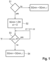
- Fig.1 shows a schematic flow diagram of a method according to the invention.
- a control variable SGmin for setting the minimum contact resistance for example a gate voltage VG (see Fig.3 )
- a power semiconductor element for example a MOSFET 1, 2 (see Fig.4 ) is to be set to a target value ZW which deviates from a recommended value SGmin_r for setting a minimum contact resistance and leads to a reduction in the minimum contact resistance compared to the contact resistance which is set when the control variable SGmin is set to the recommended value SGmin_r.
- a control variable SGmin for setting the minimum contact resistance for example a gate voltage VG (see Fig.3 )
- a power semiconductor element for example a MOSFET 1, 2 (see Fig.4 ) is to be set to a target value ZW which deviates from a recommended value SGmin_r for setting a minimum contact resistance and leads to a reduction in the minimum contact resistance compared to the contact resistance which is set when the
- control variable SGmin is set to the target value in a second step S2 and a time counter value is set to the value ct equal to zero.
- the control variable SGmin is set to the target value ZW for a predetermined period of time, whereby the predetermined period of time is fixedly parameterized.
- it is repeatedly checked, in particular periodically, whether the period of time with the set target value ZW is less than a predetermined and fixedly parameterized threshold value Tf or equal to this threshold value Tf.
- the threshold value Tf thus corresponds to the predetermined period of time. If this is not the case, the time counter value ct is incremented by a time increment ⁇ t and the third step S3 is carried out again.
- the control variable SGmin is set back to the recommended value SGmin_r in a fourth step S4.
- the predetermined threshold value Tf can be stored in a memory device 9 (see Fig.4 ) and retrieved from there for evaluation.
- control variable SGmin is set to the recommended value SGmin_r.
- a criterion which is checked in the first step S1 can be met if a target value of the power current through the power semiconductor element is greater than a predetermined threshold value. Another criterion can be met if a semiconductor temperature is greater than a predetermined threshold value. Another criterion can be met if an ambient temperature is greater than a predetermined threshold value.
- a further criterion can be met if a fault is detected in a power network that includes the power semiconductor element or if a predetermined operating mode of a vehicle is activated and/or if a state of charge of a traction battery of the vehicle is less than a predetermined threshold value, wherein the power semiconductor element is part of a traction network of the vehicle.
- control variable it is also possible for the control variable to be set to the target value ZW if activation occurs through user input and/or through a system external to the vehicle, whereby a corresponding criterion can also be met in this case.
- Fig.2 shows a schematic flow diagram of a method according to the invention in a further embodiment.
- the sum of the time periods in which the control variable SGmin for reducing the volume resistance was already set to the target value ZW is determined. If this sum is smaller than a further predetermined threshold value Tsum or equal to this threshold value Tsum, the method is continued with the method described in Fig.1 The control continues with the third step S3 shown. However, if the sum is greater than the predetermined threshold value Tsum, the control variable SGmin is set to the recommended value SGmin_r and the control variable SGmin is not set to the target value ZW.
- Fig.3 shows a schematic temporal progression of a control variable, namely a gate voltage VG of a MOSFET 1, 2 (see Fig.4 ).
- the MOSFET 1, 2 can be part of a power converter, for example, which in turn can provide an alternating voltage for operating an electrical machine, for example a traction machine in an electric or hybrid vehicle.
- the MOSFET 1, 2 can be operated in a clocked manner, with the gate voltage VG being switched with a duty cycle, which can be determined by a higher-level system, between a value for setting a minimum resistance and a value for setting a maximum resistance.
- a recommended value of the control variable SGmin_r for setting a minimum contact resistance i.e. the recommended minimum contact resistance
- a recommended value for setting a maximum contact resistance is -4 V.
- a first time t1 it is detected, for example, since the signal obtained in a first step S1 (see Fig.1 or Fig.2 ) tested criterion is met that the control variable SGmin is to be set to a target value ZW to set a minimum contact resistance, whereby the minimum contact resistance is further reduced compared to the contact resistance with the recommended control variable SGmin_r set.
- the target value ZW is, for example, +18 V. It is also shown that this control variable SGmin remains set to the target value ZW until a second time t2, whereby the time difference between the second and the first time t2, t1 corresponds to the predetermined threshold value Tf, which can be, for example, 10 or 20 seconds.
- Fig.4 shows a schematic block diagram of a device 3 according to the invention.
- the device 3 serves to operate a power semiconductor element with an adjustable contact resistance for a power current, e.g. to operate a MOSFET 1, 2.
- the power semiconductor element can be part of a power network, which can be e.g. a traction network of an electric or hybrid vehicle.
- the power network can comprise an intermediate circuit capacitor CZ.
- a first MOSFET 1 can be a so-called high-side MOSFET and a second MOSFET 2 can be a so-called low-side MOSFET of a half-bridge of a power converter, the MOSFETs 1, 2 being operated in such a way that a direct voltage in an intermediate circuit 4 is converted into an alternating voltage of a phase line 5.
- the device 3 comprises a first device 6 for providing a control variable for setting the contact resistance of the first MOSFET 1 and a second device 7 for setting the contact resistance of the second MOSFET 2.
- Such devices 6, 7 are known to those skilled in the art and can comprise electrical or electronic components for providing a control variable, e.g. in the form of a gate voltage VG.
- the device 3 also comprises a control device 8, which is e.g. in the form of a microcontroller or integrated circuit or can comprise one of these. This control device controls the devices 6, 7 in such a way that they provide a desired temporal progression of the control variable.
- a power supply device for supplying the devices 6, 7, whereby this provides the desired control variable from the power supply device, for example a capacitor or an energy storage device different therefrom.
- the evaluation device 8 can evaluate the criterion(s) that were determined in the first step S1 of the Fig.1 shown method. If the criteria are met, the control device 8 can control the first device 6, the second device 7 or both devices 6, 7 in such a way that a target value ZW (see e.g. Fig.1 ), whereby - as already explained - this deviates from a recommended value SGmin_r for setting a recommended minimum contact resistance.
- control device 8 can in particular change a setpoint value for the control variable provided by the device 6, 7, which is an output variable of this device 6, 7, e.g. from a value of +15V to the value +18V.
- the predetermined time period is permanently parameterized and stored in a memory device 9 of the device 3 and is retrieved from this at runtime.
- Fig.5 shows a schematic block diagram of a device 3 according to the invention in a further embodiment.
- the device 3 comprises a device 10 for providing an additional control variable. If the criteria that were determined in the first step S1 (see Fig.1 ) is/are checked, the control device 8 can control the first device 6 in such a way that it provides the recommended value SGmin_r for setting a minimum contact resistance. The control device 8 can also control the device 10 for providing an additional control variable in such a way that it provides the difference between the target value ZW and the output value provided by the device 6 for generating the control variable or the recommended value SGmin_r.
- the control device 8 can control the device 10 for providing an additional control variable in such a way that it generates an additional voltage of +3V.
- the output variable provided by the device 10 for providing an additional control variable can then be additively superimposed on the output variable provided by the first device 6.
Landscapes
- Engineering & Computer Science (AREA)
- Power Engineering (AREA)
- Physics & Mathematics (AREA)
- General Physics & Mathematics (AREA)
- Transportation (AREA)
- Mechanical Engineering (AREA)
- Power Conversion In General (AREA)
Applications Claiming Priority (1)
| Application Number | Priority Date | Filing Date | Title |
|---|---|---|---|
| DE102022210647.4A DE102022210647A1 (de) | 2022-10-10 | 2022-10-10 | Verfahren und Vorrichtung zum Betrieb eines Leistungshalbleiterelements |
Publications (1)
| Publication Number | Publication Date |
|---|---|
| EP4354732A1 true EP4354732A1 (fr) | 2024-04-17 |
Family
ID=88020731
Family Applications (1)
| Application Number | Title | Priority Date | Filing Date |
|---|---|---|---|
| EP23197107.8A Pending EP4354732A1 (fr) | 2022-10-10 | 2023-09-13 | Procédé et dispositif de fonctionnement d'un élément semi-conducteur de puissance |
Country Status (3)
| Country | Link |
|---|---|
| EP (1) | EP4354732A1 (fr) |
| CN (1) | CN117879325A (fr) |
| DE (1) | DE102022210647A1 (fr) |
Families Citing this family (1)
| Publication number | Priority date | Publication date | Assignee | Title |
|---|---|---|---|---|
| DE102024119755A1 (de) * | 2024-07-11 | 2026-01-15 | Voith Patent Gmbh | Verfahren zum Schalten eines Gate-Treibers, Verfahren zum Ansteuern eines Transistors, Gate-Treiber, Spannungsversorgung für einen Synchronmotor und Antriebssystem mit einem Synchronmotor |
Citations (6)
| Publication number | Priority date | Publication date | Assignee | Title |
|---|---|---|---|---|
| US20090001915A1 (en) | 2007-06-28 | 2009-01-01 | Welchko Brian A | Method and apparatus for active voltage control of electric motors |
| US20110007536A1 (en) | 2008-03-18 | 2011-01-13 | Toyota Jidosha Kabushiki Kaisha | Device for driving inverter |
| US20190149145A1 (en) | 2017-11-14 | 2019-05-16 | Ford Global Technologies, Llc | Variable resistance power switch feedback |
| DE102017127752A1 (de) * | 2017-11-23 | 2019-05-23 | Infineon Technologies Ag | Verfahren und elektronische schaltung zum ansteuern einestransistorbauelements |
| US10505538B1 (en) | 2019-02-06 | 2019-12-10 | GM Global Technology Operations LLC | Dynamic gate drive system and control method |
| WO2021047768A1 (fr) | 2019-09-11 | 2021-03-18 | Kone Corporation | Procédé de réduction de contrainte thermique d'un commutateur à semi-conducteur de puissance, unité convertisseur électrique et ascenseur |
Family Cites Families (1)
| Publication number | Priority date | Publication date | Assignee | Title |
|---|---|---|---|---|
| EP3576270A1 (fr) | 2018-05-29 | 2019-12-04 | Siemens Aktiengesellschaft | Onduleur à tension de commande de grille avec une tension élevé à température de la couche d'arrêt élevée |
-
2022
- 2022-10-10 DE DE102022210647.4A patent/DE102022210647A1/de active Pending
-
2023
- 2023-09-13 EP EP23197107.8A patent/EP4354732A1/fr active Pending
- 2023-10-09 CN CN202311304048.7A patent/CN117879325A/zh active Pending
Patent Citations (6)
| Publication number | Priority date | Publication date | Assignee | Title |
|---|---|---|---|---|
| US20090001915A1 (en) | 2007-06-28 | 2009-01-01 | Welchko Brian A | Method and apparatus for active voltage control of electric motors |
| US20110007536A1 (en) | 2008-03-18 | 2011-01-13 | Toyota Jidosha Kabushiki Kaisha | Device for driving inverter |
| US20190149145A1 (en) | 2017-11-14 | 2019-05-16 | Ford Global Technologies, Llc | Variable resistance power switch feedback |
| DE102017127752A1 (de) * | 2017-11-23 | 2019-05-23 | Infineon Technologies Ag | Verfahren und elektronische schaltung zum ansteuern einestransistorbauelements |
| US10505538B1 (en) | 2019-02-06 | 2019-12-10 | GM Global Technology Operations LLC | Dynamic gate drive system and control method |
| WO2021047768A1 (fr) | 2019-09-11 | 2021-03-18 | Kone Corporation | Procédé de réduction de contrainte thermique d'un commutateur à semi-conducteur de puissance, unité convertisseur électrique et ascenseur |
Also Published As
| Publication number | Publication date |
|---|---|
| DE102022210647A1 (de) | 2024-04-11 |
| CN117879325A (zh) | 2024-04-12 |
Similar Documents
| Publication | Publication Date | Title |
|---|---|---|
| DE19732828C2 (de) | Schaltungsanordnung zur Ansteuerung eines Leuchtdioden-Arrays | |
| DE102012219646A1 (de) | Halbleitervorrichtung, die eine an ein Halbleiterschaltelement angelegte Spannung misst | |
| DE102014202717B3 (de) | System zur Kapazitätsbestimmung eines Zwischenkreiskondensators und Verfahren zum Ansteuern eines Wechselrichters | |
| DE102017128256A1 (de) | Gatetreiber mit temperaturkompensiertem abschalten | |
| EP3748827B1 (fr) | Convertisseur demi-pont avec tension de grille reduite pendant les temps morts | |
| WO2019158748A1 (fr) | Dispositif de décharge, unité électrique et procédé de décharge | |
| DE102022120065A1 (de) | Verfahren zum reduzieren einer oszillation während des anschaltens eines leistungstransistors durch regeln der gate-schaltgeschwindigkeitssteuerung seines komplementären leistungstransistors | |
| DE102015219683B4 (de) | Entladungsvorrichtung | |
| EP4354732A1 (fr) | Procédé et dispositif de fonctionnement d'un élément semi-conducteur de puissance | |
| DE102024203020A1 (de) | Redundante aktive Entladeschaltung, Steuerverfahren dafür und Wechselrichter | |
| DE102018213130A1 (de) | Elektrisches Bordnetz und Kraftfahrzeug mit einem solchen Bordnetz | |
| DE102017120399A1 (de) | Schaltvorrichtung | |
| DE102012200234A1 (de) | Verfahren und Einrichtung zur Steuerung der Ausschaltgeschwindigkeit eines Halbleiterschalters | |
| DE102014226165A1 (de) | Adaptiver Treiber für einen Transistor | |
| DE102023210890A1 (de) | Verfahren und Vorrichtung zum Betrieb eines Leistungshalbleiterelements | |
| DE112022007572T5 (de) | Halbleitervorrichtung und Leistungsumwandlungseinrichtung | |
| DE102021101382A1 (de) | Universelle klemmschaltung für schalter-gate-antriebe von kraftfahrzeugen | |
| DE102021212348B3 (de) | Verfahren zum Ansteuern von Halbleiterschaltern mindestens einer Halbbrücke und Schaltungsanordnung | |
| EP0450126B1 (fr) | Dispositif pour protéger et surveiller une résistance à impulsion pour un circuit intermédiaire de convertisseur de tension | |
| DE102019218348A1 (de) | Elektrische heizvorrichtung für ein kraftfahrzeug | |
| DE102024210347A1 (de) | Stromrichteranordung, Verfahren zum Betreiben einer Antriebseinheit und An-triebseinheit | |
| EP2909935B1 (fr) | Procédé et circuit pour la commande d'un commutateur statique | |
| DE102023211765A1 (de) | Entladungsvorrichtung zur Entladung eines Hochspannungskreises sowie ein Verfahren zum Entladen eines Hochspanungskreises | |
| WO2025114191A1 (fr) | Dispositif de commande pour commutateur à semi-conducteur d'un onduleur et procédé d'activation d'un onduleur ; décharge active d'un circuit hv par l'intermédiaire d'impulsions de synchronisation | |
| DE102024105223A1 (de) | Stromrichtervorrichtung zum Ansteuern einer elektrischen Maschine und Verfahren zum Betreiben der Energieversorgungsschaltung einer Stromrichtervorrichtung |
Legal Events
| Date | Code | Title | Description |
|---|---|---|---|
| PUAI | Public reference made under article 153(3) epc to a published international application that has entered the european phase |
Free format text: ORIGINAL CODE: 0009012 |
|
| STAA | Information on the status of an ep patent application or granted ep patent |
Free format text: STATUS: THE APPLICATION HAS BEEN PUBLISHED |
|
| AK | Designated contracting states |
Kind code of ref document: A1 Designated state(s): AL AT BE BG CH CY CZ DE DK EE ES FI FR GB GR HR HU IE IS IT LI LT LU LV MC ME MK MT NL NO PL PT RO RS SE SI SK SM TR |
|
| STAA | Information on the status of an ep patent application or granted ep patent |
Free format text: STATUS: REQUEST FOR EXAMINATION WAS MADE |
|
| 17P | Request for examination filed |
Effective date: 20241017 |
|
| RBV | Designated contracting states (corrected) |
Designated state(s): AL AT BE BG CH CY CZ DE DK EE ES FI FR GB GR HR HU IE IS IT LI LT LU LV MC ME MK MT NL NO PL PT RO RS SE SI SK SM TR |