EP4362105A2 - Rückseitige barriere für transistoren auf galliumnitridbasis mit hoher elektronenmobilität - Google Patents
Rückseitige barriere für transistoren auf galliumnitridbasis mit hoher elektronenmobilität Download PDFInfo
- Publication number
- EP4362105A2 EP4362105A2 EP23203382.9A EP23203382A EP4362105A2 EP 4362105 A2 EP4362105 A2 EP 4362105A2 EP 23203382 A EP23203382 A EP 23203382A EP 4362105 A2 EP4362105 A2 EP 4362105A2
- Authority
- EP
- European Patent Office
- Prior art keywords
- layer
- ingan
- gan
- barrier
- algan
- Prior art date
- Legal status (The legal status is an assumption and is not a legal conclusion. Google has not performed a legal analysis and makes no representation as to the accuracy of the status listed.)
- Pending
Links
Images

Classifications
-
- H—ELECTRICITY
- H10—SEMICONDUCTOR DEVICES; ELECTRIC SOLID-STATE DEVICES NOT OTHERWISE PROVIDED FOR
- H10D—INORGANIC ELECTRIC SEMICONDUCTOR DEVICES
- H10D30/00—Field-effect transistors [FET]
- H10D30/40—FETs having zero-dimensional [0D], one-dimensional [1D] or two-dimensional [2D] charge carrier gas channels
- H10D30/47—FETs having zero-dimensional [0D], one-dimensional [1D] or two-dimensional [2D] charge carrier gas channels having two-dimensional [2D] charge carrier gas channels, e.g. nanoribbon FETs or high electron mobility transistors [HEMT]
- H10D30/471—High electron mobility transistors [HEMT] or high hole mobility transistors [HHMT]
- H10D30/473—High electron mobility transistors [HEMT] or high hole mobility transistors [HHMT] having confinement of carriers by multiple heterojunctions, e.g. quantum well HEMT
- H10D30/4732—High electron mobility transistors [HEMT] or high hole mobility transistors [HHMT] having confinement of carriers by multiple heterojunctions, e.g. quantum well HEMT using Group III-V semiconductor material
-
- H—ELECTRICITY
- H10—SEMICONDUCTOR DEVICES; ELECTRIC SOLID-STATE DEVICES NOT OTHERWISE PROVIDED FOR
- H10D—INORGANIC ELECTRIC SEMICONDUCTOR DEVICES
- H10D30/00—Field-effect transistors [FET]
- H10D30/40—FETs having zero-dimensional [0D], one-dimensional [1D] or two-dimensional [2D] charge carrier gas channels
- H10D30/47—FETs having zero-dimensional [0D], one-dimensional [1D] or two-dimensional [2D] charge carrier gas channels having two-dimensional [2D] charge carrier gas channels, e.g. nanoribbon FETs or high electron mobility transistors [HEMT]
- H10D30/471—High electron mobility transistors [HEMT] or high hole mobility transistors [HHMT]
- H10D30/475—High electron mobility transistors [HEMT] or high hole mobility transistors [HHMT] having wider bandgap layer formed on top of lower bandgap active layer, e.g. undoped barrier HEMTs such as i-AlGaN/GaN HEMTs
-
- H—ELECTRICITY
- H10—SEMICONDUCTOR DEVICES; ELECTRIC SOLID-STATE DEVICES NOT OTHERWISE PROVIDED FOR
- H10D—INORGANIC ELECTRIC SEMICONDUCTOR DEVICES
- H10D62/00—Semiconductor bodies, or regions thereof, of devices having potential barriers
- H10D62/80—Semiconductor bodies, or regions thereof, of devices having potential barriers characterised by the materials
- H10D62/82—Heterojunctions
- H10D62/824—Heterojunctions comprising only Group III-V materials heterojunctions, e.g. GaN/AlGaN heterojunctions
-
- H—ELECTRICITY
- H10—SEMICONDUCTOR DEVICES; ELECTRIC SOLID-STATE DEVICES NOT OTHERWISE PROVIDED FOR
- H10D—INORGANIC ELECTRIC SEMICONDUCTOR DEVICES
- H10D62/00—Semiconductor bodies, or regions thereof, of devices having potential barriers
- H10D62/80—Semiconductor bodies, or regions thereof, of devices having potential barriers characterised by the materials
- H10D62/85—Semiconductor bodies, or regions thereof, of devices having potential barriers characterised by the materials being Group III-V materials, e.g. GaAs
- H10D62/8503—Nitride Group III-V materials, e.g. AlN or GaN
Definitions
- This disclosure relates generally to a gallium nitride (GaN) based high electron mobility transistor (HEMT) and, more particularly, to a GaN based HEMT including a low Al % AlGaN buffer layer and a thin InGaN layer.
- GaN gallium nitride
- HEMT high electron mobility transistor
- FET Field-effect transistors
- a typical FET will include various semiconductor layers, such as silicon, gallium arsenide (GaAs), indium gallium arsenide (InGaAs), indium aluminum arsenide (InAIAs), gallium nitride (GaN), indium phosphide (InP), etc.
- the semiconductor layers are doped with various impurities, such as boron and silicon, to increase the population of carriers in the layer, where the higher the doping level of the layer the greater the conductivity of the particular semiconductor material.
- An FET will also include a source terminal, a drain terminal and a gate terminal, where one or more of the semiconductor layers is a channel layer and is in electrical contact with the source and drain terminals.
- An electrical potential difference applied between the source and drain terminals allows electrical carriers, either N-type or P-type, to flow through the channel layer between the source and drain terminals.
- An electric signal applied to the gate terminal creates an electrical field that modulates the carriers in the channel layer, where a small change in the gate voltage can cause a large variation in the population of carriers in the channel layer to change the current flow from between the source terminal and drain terminals.
- HEMT devices are popular transistor devices that have many applications, especially high frequency or high-speed applications.
- GaN HEMT devices are typically epitaxialy grown on a suitable substrate, such as silicon carbide (SiC), sapphire, silicon, etc., all well known to those skilled in the art.
- a typical HEMT device may have a SiC substrate that includes alternating crystalline layers of silicon and carbon.
- a nucleation layer such as an AIN layer, is often deposited on the SiC substrate to help facilitate epitaxial growth, where the nucleation layer is grown on the side of the substrate having a silicon face so that the orientation of the crystalline structure of the nucleation layer, and the subsequent device layers, has a gallium orientation.
- a buffer layer is typically grown on the nucleation layer that provides a crystalline structure having limited defects, where the buffer layer is typically GaN or low Al % AlGaN.
- a GaN channel layer is deposited on the buffer layer and an AlGaN barrier layer is deposited on the channel layer, where a two-dimensional electron gas (2-DEG) layer for the flow of electrons is created at the interface between the channel layer and the barrier layer.
- 2-DEG two-dimensional electron gas
- the first approach employs a thin InGaN layer between the GaN channel layer and the GaN buffer layer, and the second approach grows the GaN channel layer on top of a low Al % AlGaN buffer layer.
- the first approach produces a higher breakdown voltage and a lower thermal resistance from the channel layer to the backside of the wafer than the second approach.
- the turn-off characteristics of the HEMT for the first approach is not as sharp as the second approach. At low voltages, this translates into a lower transconductance, a more negative pinch-off voltage and a lower RF gain of the HEMT than the second approach.
- the second approach produces a lower breakdown voltage and a higher thermal resistance from the channel layer to backside of wafer compared to the first approach.
- the first approach uses polarization in the thin InGaN layer to create the voltage independent conduction band back-barrier and it is typically located at least 10 nm from the AIGaN/GaN interface.
- the Fermi-level needs to be used. Since the InGaN conduction band crosses the Fermi-level, some electrons exist in the InGaN layer, which results in a transition from the HEMT's off-state to on-state that is less steep with the gate voltage compared to HEMT's without the InGaN layer.
- the second approach grows the GaN channel layer on a low Al % AlGaN.
- the difference in the lattice constants between the AlGaN and the GaN produces a net polarization charge at the GaN channel/AIGaN buffer interface.
- This polarization charge produces an electric field in the channel layer that further confines the electrons to the AlGaN barrier/GaN channel interface.
- the conduction band increase in the channel layer is the polarization electric field time the thickness of the channel layer. This results in a thickness of ⁇ 50nm to produce a large conduction band rise in the channel layer.
- the conduction band discontinuity between the AlGaN buffer layer and the GaN channel layer contributes very little to any confinement of electrons in the channel layer.
- the drain voltage increases, short channel effects can occur and an electric field due to the drain voltage can offset the electric field due to polarization.
- confinement of electrons in the channel layer is reduced and the AlGaN buffer layer approach is no longer effective. This results in a lower breakdown voltage compared to the first approach.
- this disclosure proposes an HEMT that provides improvements in the confinement of electrons in the device channel layer for all voltages during operation of the HEMT, which leads to improved RF performance of the HEMT over known devices.
- the new approach inserts a thin InGaN layer into the GaN channel layer that is grown on a low Al % AlGaN buffer layer.
- the polarization electric field due to the lattice constant difference between the GaN layer and the AlGaN buffer layer prevents the conduction band of the InGaN layer from crossing the Fermi level and maintains the steep transition from the off-state to the on-state with gate voltage obtained from the second approach discussed above.
- the polarization electric field may be offset by an electric field produced by the drain voltage, and the confinement of electrons to the channel layer is now provided by a conduction band barrier produced by the thin InGaN layer. This results in breakdown voltages that are higher than the second approach could produce for the same design.
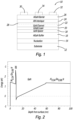
- FIG. 1 is a device profile of an HEMT device 10 including a substrate 12 on which the various epitaxial or device layers of the HEMT device 10 are deposited or grown using known epitaxial growth techniques.
- the substrate 12 can be any substrate suitable for the purposes discussed herein, such as SiC, sapphire, GaN, AIN, Si, etc.
- a nucleation layer 14 is grown on the substrate 12 to provide a base layer for proper epitaxial growth of the device layers, and can be, for example, GaN, AlGaN or AIN.
- An AlGaN buffer layer 16 is grown on the nucleation layer 14, and for reasons that will be discussed below has a low percentage, for example, 1% - 6%, of Al.
- the buffer layer 16 is Al 0.04 Ga 0.96 N.
- a GaN spacer layer 18 is grown on the buffer layer 16 and a thin InGaN layer 20 is grown on the spacer layer 18 having a thickness that is less than 20 nm.
- the thin layer 20 is In 0.1 Ga 0.9 N, is about 2 nm thick and has an In composition of about 10%.
- a GaN channel layer 22 is grown on the thin layer 20 and an optional AIN interlayer 24 is grown on the channel layer 22.
- An AlGaN barrier layer 26 is grown on the interlayer 24, where the piezoelectric/spontaneous polarization effect between the AlGaN barrier layer 26 and the GaN channel layer 22 generates a 2-DEG layer 28 between the interlayer 24 and the channel layer 22.
- the barrier layer 26 is Al 0.34 Ga 0.66 N. Suitable patterning and metal deposition steps are performed to provide a source terminal 30, a drain terminal 32 and a gate terminal 34 on the barrier layer 26.
- FIG. 2 is a conduction band diagram of the AlGaN HEMT device 10, but where the thin InGaN layer 20 has been removed
- FIG. 3 is a conduction band diagram of the AlGaN HEMT device 10, but where the low Al % AlGaN buffer layer 16 is replaced with a GaN buffer layer
- FIG. 4 is a conduction band diagram of the AlGaN HEMT device 10.
- the primary confinement mechanism to keep electrons at the interface between the barrier layer 26 and the interlayer 24 is the polarization induced electric field that results from the lattice constant mismatch between the GaN channel layer 22 and the low Al % AlGaN buffer layer 16. This electric field can be offset by short channel effects at high drain voltages, which then results in low breakdown voltage.
- the thin InGaN layer 20 produces a barrier in the conduction band between the GaN channel layer 22 and the GaN buffer layer that replaced the buffer layer 16.
- an In % of about 10 % is used in the layer 20, but this results in the conduction band in the InGaN layer 20 crossing the Fermi level.
- the conduction band of the InGaN layer 20 is close to the Fermi level, electrons begin to populate the layer 20, which produces a less steep transition from the off-state to the on-state with the gate voltage. This results in a more negative pinch-off voltage, smaller transconductance and a lower RF gain.
- the shift in the conduction band in the thin InGaN layer 20 is due to the polarization in the thin InGaN layer 20 that is not influenced by the drain voltage. This allows confinement to high voltages (unlike the AlGaN buffer confinement approach), thus resulting in a high breakdown voltage.
- the thin InGaN layer 20 produces a barrier in the conduction band between the GaN channel layer 22 and the GaN spacer layer 18 that is not dependent on external electric fields.
- Growing the spacer layer 18 on the low Al % AlGaN buffer layer 16 produces a polarization electric field that exists in the GaN channel layer 22, the InGaN layer 20 and the GaN spacer layer 18. This polarization electric field prevents electrons from occupying the InGaN layer 26 at low voltages providing the desired steep transition from the off-state to the on-state with gate voltage, high transconductance, and high RF gain at lower voltages.
- the barrier produced in the conduction band by the InGaN layer 20 between the GaN channel layer 22 and the GaN spacer layer 18 is still present resulting in high breakdown voltage.
Landscapes
- Junction Field-Effect Transistors (AREA)
Applications Claiming Priority (1)
| Application Number | Priority Date | Filing Date | Title |
|---|---|---|---|
| US18/049,064 US20240234560A9 (en) | 2022-10-24 | 2022-10-24 | Back-barrier for gallium nitride based high electron mobility transistors |
Publications (2)
| Publication Number | Publication Date |
|---|---|
| EP4362105A2 true EP4362105A2 (de) | 2024-05-01 |
| EP4362105A3 EP4362105A3 (de) | 2024-07-31 |
Family
ID=88412204
Family Applications (1)
| Application Number | Title | Priority Date | Filing Date |
|---|---|---|---|
| EP23203382.9A Pending EP4362105A3 (de) | 2022-10-24 | 2023-10-13 | Rückseitige barriere für transistoren auf galliumnitridbasis mit hoher elektronenmobilität |
Country Status (3)
| Country | Link |
|---|---|
| US (1) | US20240234560A9 (de) |
| EP (1) | EP4362105A3 (de) |
| JP (1) | JP2024062415A (de) |
Family Cites Families (6)
| Publication number | Priority date | Publication date | Assignee | Title |
|---|---|---|---|---|
| US7612390B2 (en) * | 2004-02-05 | 2009-11-03 | Cree, Inc. | Heterojunction transistors including energy barriers |
| US8476125B2 (en) * | 2006-12-15 | 2013-07-02 | University Of South Carolina | Fabrication technique for high frequency, high power group III nitride electronic devices |
| TW200903805A (en) * | 2007-05-24 | 2009-01-16 | Univ California | Polarization-induced barriers for N-face nitride-based electronics |
| US20130207078A1 (en) * | 2012-01-18 | 2013-08-15 | Kopin Corporation | InGaN-Based Double Heterostructure Field Effect Transistor and Method of Forming the Same |
| US8981382B2 (en) * | 2013-03-06 | 2015-03-17 | Iqe Rf, Llc | Semiconductor structure including buffer with strain compensation layers |
| US9960262B2 (en) * | 2016-02-25 | 2018-05-01 | Raytheon Company | Group III—nitride double-heterojunction field effect transistor |
-
2022
- 2022-10-24 US US18/049,064 patent/US20240234560A9/en active Pending
-
2023
- 2023-10-13 EP EP23203382.9A patent/EP4362105A3/de active Pending
- 2023-10-24 JP JP2023182388A patent/JP2024062415A/ja active Pending
Also Published As
| Publication number | Publication date |
|---|---|
| US20240234560A9 (en) | 2024-07-11 |
| EP4362105A3 (de) | 2024-07-31 |
| JP2024062415A (ja) | 2024-05-09 |
| US20240136431A1 (en) | 2024-04-25 |
Similar Documents
| Publication | Publication Date | Title |
|---|---|---|
| Kim et al. | High breakdown voltage and low-current dispersion in AlGaN/GaN HEMTs with high-quality AlN buffer layer | |
| US8835986B2 (en) | Method for fabrication of III-nitride device and the III-nitride device thereof | |
| CN101689570B (zh) | 采用耗尽模式GaN基FET的串叠电路 | |
| Jiang et al. | enhancement-mode GaN MOS-HEMTs with recess-free barrier engineering and high-${k} $ ZrO2 gate dielectric | |
| US6583454B2 (en) | Nitride based transistors on semi-insulating silicon carbide substrates | |
| US6914273B2 (en) | GaN-type enhancement MOSFET using hetero structure | |
| CN101410985B (zh) | 高效率和/或高功率密度宽带隙晶体管 | |
| US8390029B2 (en) | Semiconductor device for reducing and/or preventing current collapse | |
| WO2022031465A1 (en) | Iii-nitride devices including a depleting layer | |
| CN104704608B (zh) | 氮化物半导体结构物 | |
| EP1909316A1 (de) | Transistor und verfahren zu seinem betrieb | |
| KR101092467B1 (ko) | 인헨스먼트 노말리 오프 질화물 반도체 소자 및 그 제조방법 | |
| US8669592B2 (en) | Compound semiconductor device and method for fabricating the same | |
| US20120292665A1 (en) | High performance multigate transistor | |
| US20150060873A1 (en) | Crystalline Layer for Passivation of III-N Surface | |
| JP2009231395A (ja) | 半導体装置および半導体装置の製造方法 | |
| JP7257498B2 (ja) | 窒化物半導体装置 | |
| US7465968B2 (en) | Semiconductor device and method for fabricating the same | |
| KR101200274B1 (ko) | 인헨스먼트 노멀리 오프 버티컬 질화물 반도체 소자 및 그 제조방법 | |
| KR100857683B1 (ko) | 질화물 반도체 소자 및 그 제조방법 | |
| CN106206709A (zh) | 半导体装置 | |
| US12166118B2 (en) | High electron mobility transistors (HEMTS) including a yttrium (Y) and aluminum nitride (AIN) (YAIN) alloy layer | |
| US20240234560A9 (en) | Back-barrier for gallium nitride based high electron mobility transistors | |
| CN113871478B (zh) | 基于双栅的具有p型沟道特性的新型半导体器件 | |
| Chen et al. | Indium-based ternary barrier high-electron-mobility transistors on Si substrate with high ON/OFF ratio for power applications |
Legal Events
| Date | Code | Title | Description |
|---|---|---|---|
| PUAI | Public reference made under article 153(3) epc to a published international application that has entered the european phase |
Free format text: ORIGINAL CODE: 0009012 |
|
| STAA | Information on the status of an ep patent application or granted ep patent |
Free format text: STATUS: THE APPLICATION HAS BEEN PUBLISHED |
|
| AK | Designated contracting states |
Kind code of ref document: A2 Designated state(s): AL AT BE BG CH CY CZ DE DK EE ES FI FR GB GR HR HU IE IS IT LI LT LU LV MC ME MK MT NL NO PL PT RO RS SE SI SK SM TR |
|
| PUAL | Search report despatched |
Free format text: ORIGINAL CODE: 0009013 |
|
| AK | Designated contracting states |
Kind code of ref document: A3 Designated state(s): AL AT BE BG CH CY CZ DE DK EE ES FI FR GB GR HR HU IE IS IT LI LT LU LV MC ME MK MT NL NO PL PT RO RS SE SI SK SM TR |
|
| RIC1 | Information provided on ipc code assigned before grant |
Ipc: H01L 29/20 20060101ALN20240626BHEP Ipc: H01L 29/205 20060101ALI20240626BHEP Ipc: H01L 29/778 20060101AFI20240626BHEP |
|
| STAA | Information on the status of an ep patent application or granted ep patent |
Free format text: STATUS: REQUEST FOR EXAMINATION WAS MADE |
|
| 17P | Request for examination filed |
Effective date: 20241015 |
|
| RBV | Designated contracting states (corrected) |
Designated state(s): AL AT BE BG CH CY CZ DE DK EE ES FI FR GB GR HR HU IE IS IT LI LT LU LV MC ME MK MT NL NO PL PT RO RS SE SI SK SM TR |
|
| STAA | Information on the status of an ep patent application or granted ep patent |
Free format text: STATUS: EXAMINATION IS IN PROGRESS |
|
| 17Q | First examination report despatched |
Effective date: 20260311 |