EP4376242A1 - Strombegrenzungsschaltung - Google Patents
Strombegrenzungsschaltung Download PDFInfo
- Publication number
- EP4376242A1 EP4376242A1 EP21810269.7A EP21810269A EP4376242A1 EP 4376242 A1 EP4376242 A1 EP 4376242A1 EP 21810269 A EP21810269 A EP 21810269A EP 4376242 A1 EP4376242 A1 EP 4376242A1
- Authority
- EP
- European Patent Office
- Prior art keywords
- terminal
- transistor
- voltage
- electrically connected
- unit
- Prior art date
- Legal status (The legal status is an assumption and is not a legal conclusion. Google has not performed a legal analysis and makes no representation as to the accuracy of the status listed.)
- Pending
Links
Images

Classifications
-
- H—ELECTRICITY
- H02—GENERATION; CONVERSION OR DISTRIBUTION OF ELECTRIC POWER
- H02H—EMERGENCY PROTECTIVE CIRCUIT ARRANGEMENTS
- H02H9/00—Emergency protective circuit arrangements for limiting excess current or voltage without disconnection
- H02H9/02—Emergency protective circuit arrangements for limiting excess current or voltage without disconnection responsive to excess current
-
- H—ELECTRICITY
- H02—GENERATION; CONVERSION OR DISTRIBUTION OF ELECTRIC POWER
- H02H—EMERGENCY PROTECTIVE CIRCUIT ARRANGEMENTS
- H02H9/00—Emergency protective circuit arrangements for limiting excess current or voltage without disconnection
- H02H9/02—Emergency protective circuit arrangements for limiting excess current or voltage without disconnection responsive to excess current
- H02H9/025—Current limitation using field effect transistors
-
- H—ELECTRICITY
- H02—GENERATION; CONVERSION OR DISTRIBUTION OF ELECTRIC POWER
- H02H—EMERGENCY PROTECTIVE CIRCUIT ARRANGEMENTS
- H02H3/00—Emergency protective circuit arrangements for automatic disconnection directly responsive to an undesired change from normal electric working condition with or without subsequent reconnection ; integrated protection
- H02H3/02—Details
- H02H3/025—Disconnection after limiting, e.g. when limiting is not sufficient or for facilitating disconnection
-
- H—ELECTRICITY
- H02—GENERATION; CONVERSION OR DISTRIBUTION OF ELECTRIC POWER
- H02H—EMERGENCY PROTECTIVE CIRCUIT ARRANGEMENTS
- H02H7/00—Emergency protective circuit arrangements specially adapted for specific types of electric machines or apparatus or for sectionalised protection of cable or line systems, and effecting automatic switching in the event of an undesired change from normal working conditions
- H02H7/20—Emergency protective circuit arrangements specially adapted for specific types of electric machines or apparatus or for sectionalised protection of cable or line systems, and effecting automatic switching in the event of an undesired change from normal working conditions for electronic equipment
- H02H7/205—Emergency protective circuit arrangements specially adapted for specific types of electric machines or apparatus or for sectionalised protection of cable or line systems, and effecting automatic switching in the event of an undesired change from normal working conditions for electronic equipment for controlled semi-conductors which are not included in a specific circuit arrangement
-
- H—ELECTRICITY
- H03—ELECTRONIC CIRCUITRY
- H03K—PULSE TECHNIQUE
- H03K17/00—Electronic switching or gating, i.e. not by contact-making and –breaking
- H03K17/08—Modifications for protecting switching circuit against overcurrent or overvoltage
- H03K17/082—Modifications for protecting switching circuit against overcurrent or overvoltage by feedback from the output to the control circuit
- H03K17/0822—Modifications for protecting switching circuit against overcurrent or overvoltage by feedback from the output to the control circuit in field-effect transistor switches
-
- H—ELECTRICITY
- H03—ELECTRONIC CIRCUITRY
- H03K—PULSE TECHNIQUE
- H03K17/00—Electronic switching or gating, i.e. not by contact-making and –breaking
- H03K17/16—Modifications for eliminating interference voltages or currents
- H03K17/161—Modifications for eliminating interference voltages or currents in field-effect transistor switches
- H03K17/165—Modifications for eliminating interference voltages or currents in field-effect transistor switches by feedback from the output circuit to the control circuit
- H03K17/166—Soft switching
-
- G—PHYSICS
- G09—EDUCATION; CRYPTOGRAPHY; DISPLAY; ADVERTISING; SEALS
- G09G—ARRANGEMENTS OR CIRCUITS FOR CONTROL OF INDICATING DEVICES USING STATIC MEANS TO PRESENT VARIABLE INFORMATION
- G09G2330/00—Aspects of power supply; Aspects of display protection and defect management
- G09G2330/02—Details of power systems and of start or stop of display operation
- G09G2330/025—Reduction of instantaneous peaks of current
-
- H—ELECTRICITY
- H02—GENERATION; CONVERSION OR DISTRIBUTION OF ELECTRIC POWER
- H02H—EMERGENCY PROTECTIVE CIRCUIT ARRANGEMENTS
- H02H3/00—Emergency protective circuit arrangements for automatic disconnection directly responsive to an undesired change from normal electric working condition with or without subsequent reconnection ; integrated protection
- H02H3/006—Calibration or setting of parameters
-
- H—ELECTRICITY
- H03—ELECTRONIC CIRCUITRY
- H03K—PULSE TECHNIQUE
- H03K2217/00—Indexing scheme related to electronic switching or gating, i.e. not by contact-making or -breaking covered by H03K17/00
- H03K2217/0054—Gating switches, e.g. pass gates
Definitions
- the present disclosure relates to a field of display technology, and more particularly, to a current limiting circuit.
- the disadvantage of the conventional design is that the current limiting value for the AVDD voltage is constant. If the current limiting value is excessively small, the power management integrated chip cannot establish the voltage within the specified time during booting-up under a heavy-load due to the current limiting, and, thus, the booting-up fails; if the current limiting value is excessively large, the components of the power management integrated chip are damaged by the long-term high current when the back-end load is short-circuited, for example, the source driver is damaged and on fire.
- the present disclosure provides a current limiting circuit which can make a current limiting value of the current limiting circuit adjustable, thereby preventing the power management integrated chip from causing the failed booted-up under a heavy load and further preventing the power management integrated chip from being damaged due to a short-circuited back-end load during the booting-up.
- an embodiment of the present disclosure is to provide a current limiting circuit.
- the current limiting circuit includes a first voltage terminal, a second voltage terminal, a first transistor and a current limiting module.
- An input terminal of the first transistor is electrically connected to the first voltage terminal, and an output terminal of the first transistor is electrically connected to the second voltage terminal.
- the current limiting module is electrically connected to the input terminal of the first transistor and a control terminal of the first transistor.
- the current limiting module comprises a second transistor, a first resistor, a third transistor, and a regulation unit.
- a first terminal of the second transistor is electrically connected to a first control terminal, a second terminal of the second transistor is electrically connected to the input terminal of the first transistor, and a third terminal of the second transistor is electrically connected to the control terminal of the first transistor.
- a first terminal of the first resistor is electrically connected to the input terminal of the first transistor, and a second terminal of the first resistor is electrically connected to the control terminal of the first transistor.
- a first terminal of the third transistor is electrically connected to a second control terminal, a second terminal of the third transistor is electrically connected to the control terminal of the first transistor, and a third terminal of the third transistor is connected to the regulation unit.
- the regulation unit is configured to control the state of the first transistor.
- the regulation unit comprises a plurality of resistive control sub-units which are arranged in parallel. Respective first terminals of the plurality of resistive control sub-units are electrically connected to the third terminal of the third transistor. Respective second terminals of the plurality of resistive control sub-units are electrically connected to a ground terminal, and each of the plurality of resistive control sub-units comprises a second resistor.
- the current limiting circuit further comprises a fourth transistor.
- An input terminal of the fourth transistor is electrically connected to the first voltage terminal, and an output terminal of the fourth transistor is electrically connected to the second voltage terminal.
- the current limiting circuit further comprises a timing unit, a comparison unit, and a constant current unit.
- the timing unit is electrically connected to a first terminal of the comparison unit.
- a second terminal of the comparison unit is electrically connected to the second voltage terminal.
- a third terminal of the comparison unit receives a constant voltage signal.
- a fourth terminal of the comparison unit is electrically connected to a first terminal of the constant current unit.
- a second terminal of the constant current unit is electrically connected to a control terminal of the fourth transistor.
- the timing unit is configured to output a comparison-unit control signal at intervals with a preset time.
- the comparison unit is controlled by the comparison-unit control signal to output a constant-current-unit control signal at the fourth terminal of the comparison unit to the first terminal of the constant current unit based on a voltage at the second terminal of the comparison unit and the voltage at the third terminal of the comparison unit.
- the constant current unit is controlled by the constant-current-unit control signal to output a constant current.
- the timing unit comprises a timer that is electrically connected to the first terminal of the comparison unit.
- the comparison unit comprises a comparator.
- a first terminal of the comparator is electrically connected to the timing unit.
- a second terminal of the comparator is electrically connected to the second voltage terminal.
- a third terminal of the comparator receives the constant voltage signal.
- a fourth terminal of the comparator is electrically connected to the first terminal of the constant current unit.
- the constant current unit comprises a constant current source.
- a first terminal of the constant current source is electrically to the fourth terminal of the comparison unit, a second terminal of the constant current source is electrically to the control terminal of the fourth transistor, and a third terminal of the constant current source is electrically to a ground terminal.
- a voltage value of constant voltage signal in a range between 0.85 times a voltage value of the first voltage terminal and 0.9 times the voltage value of the first voltage terminal.
- an embodiment of the present disclosure is to provide a current limiting circuit.
- the current limiting circuit includes a first voltage terminal, a second voltage terminal, a first transistor and a current limiting module.
- An input terminal of the first transistor is electrically connected to the first voltage terminal, and an output terminal of the first transistor is electrically connected to the second voltage terminal.
- the current limiting module is electrically connected to the input terminal of the first transistor and a control terminal of the first transistor.
- the current limiting module is configured to control voltage difference between the control terminal of the first transistor and the input terminal of the first transistor for controlling a state of the first transistor so that a current limiting value of the current limiting circuit is adjustable.
- the current limiting module comprises a second transistor, a first resistor, a third transistor, and a regulation unit.
- a first terminal of the second transistor is electrically connected to a first control terminal, a second terminal of the second transistor is electrically connected to the input terminal of the first transistor, and a third terminal of the second transistor is electrically connected to the control terminal of the first transistor.
- a first terminal of the first resistor is electrically connected to the input terminal of the first transistor, and a second terminal of the first resistor is electrically connected to the control terminal of the first transistor.
- a first terminal of the third transistor is electrically connected to a second control terminal, a second terminal of the third transistor is electrically connected to the control terminal of the first transistor, and a third terminal of the third transistor is connected to the regulation unit.
- the regulation unit is configured to control the state of the first transistor.
- the current limiting circuit further comprises a fourth transistor.
- An input terminal of the fourth transistor is electrically connected to the first voltage terminal, and an output terminal of the fourth transistor is electrically connected to the second voltage terminal.
- the regulation unit comprises a plurality of resistive control sub-units which are arranged in parallel. Respective first terminals of the plurality of resistive control sub-units are electrically connected to the third terminal of the third transistor. Respective second terminals of the plurality of resistive control sub-units are electrically connected to a ground terminal, and each of the plurality of resistive control sub-units comprises a second resistor.
- the current limiting circuit further comprises a timing unit, a comparison unit, and a constant current unit.
- the timing unit is electrically connected to a first terminal of the comparison unit.
- a second terminal of the comparison unit is electrically connected to the second voltage terminal.
- a third terminal of the comparison unit receives a constant voltage signal.
- a fourth terminal of the comparison unit is electrically connected to a first terminal of the constant current unit.
- a second terminal of the constant current unit is electrically connected to a control terminal of the fourth transistor.
- the timing unit is configured to output a comparison-unit control signal at intervals with a preset time.
- the comparison unit is controlled by the comparison-unit control signal to output a constant-current-unit control signal at the fourth terminal of the comparison unit to the first terminal of the constant current unit based on a voltage at the second terminal of the comparison unit and the voltage at the third terminal of the comparison unit.
- the constant current unit is controlled by the constant-current-unit control signal to output a constant current.
- the timing unit comprises a timer that is electrically connected to the first terminal of the comparison unit.
- the comparison unit comprises a comparator.
- a first terminal of the comparator is electrically connected to the timing unit.
- a second terminal of the comparator is electrically connected to the second voltage terminal.
- a third terminal of the comparator receives the constant voltage signal.
- a fourth terminal of the comparator is electrically connected to the first terminal of the constant current unit.
- the constant current unit comprises a constant current source.
- a first terminal of the constant current source is electrically to the fourth terminal of the comparison unit, a second terminal of the constant current source is electrically to the control terminal of the fourth transistor, and a third terminal of the constant current source is electrically to a ground terminal.
- a voltage value of constant voltage signal in a range between 0.85 times a voltage value of the first voltage terminal and 0.9 times the voltage value of the first voltage terminal.
- the current limiting circuit of the embodiment of the present disclosure controls the state of the first transistor through outputting a control signal by the current limiting module to the control terminal of the first transistor so that the current limiting value of the current limiting circuit are adjustable, thereby preventing the power management integrated chip from causing the failed booted-up under a heavy load and further preventing the power management integrated chip from being damaged due to a short-circuited back-end load during the booting-up.
- the current limiting circuit of the embodiment of the present disclosure controls the state of the first transistor through outputting a control signal by the current limiting module to the control terminal of the first transistor so that the current limiting value of the current limiting circuit are adjustable, thereby preventing the power management integrated chip from causing the failed booted-up under a heavy load and further preventing the power management integrated chip from being damaged due to a short-circuited back-end load during the booting-up.
- the transistors used in the embodiments of the present disclosure may include P-type transistors and/or N-type transistors.
- the gate of the P-type transistor When the gate of the P-type transistor is applied with low level voltage, the source and drain are conducted. When the gate is applied with high level voltage, the source and the drain are not conducted.
- the gate of the N-type transistor When the gate of the N-type transistor is applied with high level voltage, the source and drain are conducted. When the gate of the N-type transistor is applied with low level voltage, the source and the drain are not conducted.
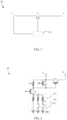
- FIG. 1 is a structural schematic diagram of a current limiting circuit according to an exemplary embodiment of the present disclosure.
- the current limiting circuit 10 comprises a first voltage terminal A, a second voltage terminal B, a first transistor T1, and a current limiting module 100.
- the input terminal of the first transistor T1 and the output terminal of the first transistor T1 are connected in series on the path formed by the first voltage terminal A and the second voltage terminal B.
- the current limiting module 100 is electrically connected to the input terminal of the first transistor T1 and the control terminal of the first transistor T1.
- the current limiting module 100 is configured to control the voltage difference between the control terminal of the first transistor T1 and the input terminal of the first transistor T1 for controlling the state of the first transistor T1 so that the current limiting value of the current limiting circuit 10 is adjustable.
- the first terminal of the first transistor T1 is one of the source and the drain of the transistor, and the second terminal of the first transistor T1 is the other of the source and the drain of the transistor.
- the control terminal is the gate of the transistor.
- the first voltage terminal A may serve as an operation voltage input terminal of a power management integrated chip
- the second voltage terminal B may serve as an AVDD voltage output terminal.
- the power management integrated chip will perform a current limiting operation during the start-up of the AVDD voltage. The purpose is to slowly turn on an isolation transistor and smoothly establish up the AVDD voltage, thereby preventing excessive currents from damaging other electronic components in the loop.
- the current limiting value of the current limiting circuit 10 is excessively small, the power management integrated chip cannot establish the voltage within the specified time during booting-up under a heavy-load due to the current limiting, and, thus, the booting-up fails; if the current limiting value of the current limiting circuit 10 is excessively large, the components of the power management integrated chip are damaged by the long-term high current when the back-end load is short-circuited.
- the current limiting value of the current limiting circuit 10 is adjustable.
- the current limiting circuit 10 of the embodiment of the present disclosure is capable of setting the current limiting value of the current limiting circuit 10 according to the actual situation, so that the current limiting value of the current limiting circuit 10 is adjusted, which prevents the power management integrated chip from causing the failed booted-up under a heavy load and further prevents the power management integrated chip from being damaged due to a short-circuited back-end load during the booting-up.
- FIG. 2 is a circuit diagram of a current limiting circuit according to an exemplary embodiment of the present disclosure.
- the current limiting module 100 comprises a second transistor T2, a first resistor R1, a third transistor T3, and a regulation unit 101.
- the first terminal of the second transistor T2 is electrically connected to a first control terminal BB.
- the second terminal of the second transistor T2 is electrically connected to the input terminal of the first transistor T1.
- the third terminal of the second transistor T2 is electrically connected to the control terminal of the first transistor T1.
- the first terminal of the first resistor R1 is electrically connected to the input terminal of the first transistor T1.
- the second terminal of the first resistor R1 is electrically connected to the control terminal of the first transistor T1.
- the first terminal of the third transistor T3 is electrically connected to a second control terminal AA.
- the second terminal of the third transistor T3 is electrically connected to the control terminal of the first transistor T1.
- the third terminal of the third transistor T3 is connected to the regulation unit 101
- the regulation unit 101 is configured to control the state of the first transistor T1.
- the regulation unit 101 comprises a plurality of resistive control sub-units 1011 which are arranged in parallel.
- the respective first terminals of the resistive control sub-units 1011 are electrically connected to the third terminal of the third transistor T3.
- the respective second terminals of the resistive control sub-units 1011 are electrically connected to a ground terminal GND.
- Each resistive control sub-unit 1011 comprises a second resistor R2.
- One of the resistive control sub-unit 1011 is provided with only a second resistor R2, while each of the other resistive control sub-units 1011 comprises a second resistor R2 and a switch S, wherein the second resistor R2 and the switch S are connected in series.
- Both the first transistor T1 and the second transistor T2 are implemented by P-type transistors, and the third transistor T3 is implemented by an N-type transistor.
- the following description will be made by taking the transistor type in the embodiment of the present disclosure as an example.
- FIG. 3 is a schematic diagram showing a first state of the current limiting circuit according to an embodiment of the present disclosure.
- the voltage at the second control terminal AA is a low potential which causes the third transistor T3 to be turned off
- the voltage at of the first control terminal BB is a low potential which causes the second transistor T2 to be turned on.
- the potential of the node x1 is equal to the potential of the node y1
- the potential of the control terminal of the first transistor T1 is equal to the potential of the node y1
- the first transistor T1 is inactivated.
- FIG. 4 is a schematic diagram showing a second state of the current limiting circuit according to an embodiment of the present disclosure.
- the voltage at the second control terminal AA is a high potential which causes the third transistor T3 to be turned on
- the potential of the first control terminal BB is a high potential which causes the second transistor T2 to be turned off.
- the potential of the node x2 is equal to the potential of the input terminal of the first transistor T1.
- the potential of the control terminal of the first transistor T1 is equal to the potential of the node y2.
- Vgs represents the voltage difference between the control terminal of the first transistor T1 and the input terminal of the first transistor T1
- V1 represents the voltage value of the input terminal of the first transistor T1
- R1 represents the resistance value of the first resistor R1
- Rx represents the resistance value of x resistive control sub-units 1011 arranged in parallel.
- the current limiting circuit 10 controls the voltage difference between the control terminal of the first transistor T1 and the input terminal of the first transistor T1 through controlling the state of the first transistor T1 by the current limiting module 100 so that the current limiting value of the current limiting circuit 10 is adjustable, thereby which prevents the power management integrated chip from causing the failed booted-up under a heavy load and further prevents the power management integrated chip from being damaged due to a short-circuited back-end load during the booting-up.
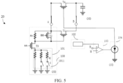
- FIG. 5 is a circuit diagram of a current limiting circuit 20 according to another exemplary embodiment of the present disclosure. Different from the current limiting circuit 10 shown in FIG. 2 , the current limiting circuit 20 further comprises a fourth transistor T4, a timing unit 102, a comparison unit 103, and a constant current unit 104.
- the input terminal of the fourth transistor T4 is electrically connected to the first voltage terminal A.
- the output terminal of the fourth transistor T4 is electrically connected to the second voltage terminal B.
- the timing unit 102 is electrically connected to the first terminal of the comparison unit 103.
- the second terminal of the comparison unit 103 is electrically connected to the second voltage terminal B.
- the third terminal of the comparison unit 103 receives a constant voltage signal M.
- the fourth terminal of the comparison unit 103 is electrically connected to the first terminal of the constant current unit 104.
- the second terminal of the constant current unit 104 is electrically connected to the control terminal of the fourth transistor T4.
- the timing unit 102 is configured to output a comparison-unit control signal at intervals with a preset time.
- the comparison unit 103 is controlled by the comparison-unit control signal to output a constant-current-unit control signal at the fourth terminal of the comparison unit 103 to the first terminal of the constant current unit 104 based on the voltage at the second terminal of the comparison unit 103 and the voltage at the third terminal of the comparison unit 103.
- the constant current unit 104 is controlled by the constant-current-unit control signal to output a constant current.
- the timing unit 102 operates as a register for setting the current limiting time. That is, the timing unit 102 is configured to output the comparison-unit control signal at intervals with a preset time.
- the constant current unit 104 starts to operate; when the first terminal of the constant current unit 104 does not receive the constant-current-unit control signal, the constant current unit 104 stops operating.
- the function of the comparison unit 103 is to compare magnitudes of two voltages (using a high or low level of an output voltage to indicate the relationship between the magnitudes of the two input voltages).
- the voltage comparator When the voltage at the "positive (+)" input terminal is higher than the voltage at the "negative (-)” input terminal, the voltage comparator outputs a high-level signal; when the voltage at the "+” input terminal is lower than the voltage at the "-” input terminal, the voltage comparator outputs a low-level voltage.
- the comparison unit 103 compares the voltage at the second terminal and the voltage at the third terminal and outputs the constant-current-unit control signal at the fourth terminal of the comparison unit 103 to the first terminal of the constant current unit 104.
- the first terminal of the comparison unit 103 is an enable terminal
- the second terminal of the comparison unit 103 is a " positive (+)" input terminal
- the third terminal of the comparison unit 103 is a " negative (-)” input terminal
- the fourth terminal of the comparison unit 103 is an output terminal.
- the constant-current-unit control signal output by the fourth terminal of the comparison unit 103 is at a high voltage level; when the voltage at the second terminal of the comparison unit 103 is lower than the voltage at the third terminal of the comparison unit 103, the constant-current-unit control signal output by the fourth terminal of the comparison unit 103 is at a low voltage level.
- the constant current unit 104 provide a constant current, which is independent of the voltage across the two terminals, to the outside.
- the constant current unit 104 has two basic properties: first, the current provided by the constant current unit 104 is constant and independent of the voltage cross the two terminals; second, the current of the constant current unit 104 is determined, and the voltage across the two terminals are arbitrary. That is, the constant current unit 104 is controlled by the control signal of the constant current unit 104 output a constant current.
- the timing unit 102 comprises a timer.
- the timer is electrically connected to the first terminal of the comparison unit 103.
- the timer outputs a high voltage signal every interval with a preset time.
- the timer can be set to different detection time scales, such as 4 milliseconds, 6 milliseconds, 8 milliseconds, or 10 milliseconds.
- the comparison unit 103 comprises a comparator.
- the first terminal of the comparator is electrically connected to the timing unit 102.
- the second terminal of the comparator is electrically connected to the second voltage terminal B.
- the third terminal of the comparator receives the constant voltage signal M.
- the fourth terminal of the comparator is electrically connected to the first terminal of the constant current unit 104.
- the first terminal of the comparator is an enable terminal
- the second terminal of the comparator is a "positive (+)” input terminal
- the third terminal of the comparator is a “negative (-)” input terminal
- the fourth terminal of the comparator is an output terminal.
- the constant-current-unit control signal output by the fourth terminal of the comparator is at a high voltage level; when the voltage at the second terminal of the comparator is less than the voltage at the third terminal of the comparator, the constant-current-unit control signal output by the output terminal of the comparator is at a low voltage level.
- the comparator is configured to compare the voltage at the second voltage terminal B with the voltage of the constant voltage signal M. When the voltage at the second voltage terminal B is higher than the voltage of the constant voltage signal M, the comparator outputs a high-level voltage; when the voltage at the second voltage terminal B is lower than the voltage of the constant voltage signal M, the comparator outputs a low-level voltage.
- the voltage value of the constant voltage signal M is in a range between 0.85 times the voltage value of the first voltage terminal A and 0.9 times the voltage value of the first voltage terminal A.
- the voltage value of the constant voltage signal M may be set to a value between 0.85 times the voltage value of the first voltage terminal A and 0.9 times the voltage value of the first voltage terminal A.
- a multiplier may be connected in series between the first voltage terminal A and the third terminal of the comparison unit 103, so that the voltage value of the constant voltage signal M is equal to a value between 0.85 times the voltage value of the first voltage terminal A and 0.9 times the voltage value of the first voltage terminal A.
- the timer is a register for setting the current limiting time, and the current limiting time is currently set to 4 milliseconds.
- the voltage value of the second voltage terminal B is compared with 0.9 times the voltage of the first voltage terminal A. If the voltage value of the second voltage terminal B is less than 0.9 times the voltage of the first voltage terminal A, the back-end load is abnormal.
- the voltage level of the control terminal of the second transistor T2 is switched to a low level from a high level, the second transistor T2 is turned on, the first transistor T1 is turned off, the constant current source is inactivated, and the power management integrated chip stops operating. If the voltage value of the second voltage terminal B is greater than 0.9 times the voltage of the first voltage terminal A, the circuit functions normally. At this time, the voltage level of the control terminal of the second transistor T2 is switched to a low level from a high level, the second transistor T2 is turned on, the first transistor T1 is turned off, the constant current source is activated, the voltage at the control terminal of the fourth transistor T4 is pulled down, and the fourth transistor T4 is turned on.
- the external fourth transistor T4 performs the isolation operation of the current limiting circuit.
- the first transistor T1 and the current limiting module 100 are disposed in the power management integrated chip.
- the fourth transistor T4, the timing unit 102, comparison unit 103, and the constant current unit 104 are disposed outside the power management integrated chip.
- the first transistor and the current limiting unit are disposed in the power management integrated chip, which results in that the accuracy of the current limit value can be guaranteed under conditions of both high and low temperature due to their good temperature characteristics and high precision. Since the resistance and the Vgs-Id curve of the first transistor do not change much with the temperature, the present disclosure has relatively better temperature characteristics, and the stability of the current limit value can be guaranteed at both high temperature (85°C) and low temperature (-20°C).
- the current limiting circuit of the embodiments of the present disclosure outputs a control signal to the control terminal of the isolation transistor to control the state of the isolation transistor so that the current limiting value and the current limiting time of the current limiting circuit are adjustable, thereby preventing the power management integrated chip from causing the failed booted-up under a heavy load and further preventing the power management integrated chip from being damaged due to a short-circuited back-end load during the booting-up.
Landscapes
- Engineering & Computer Science (AREA)
- Power Engineering (AREA)
- Emergency Protection Circuit Devices (AREA)
- Continuous-Control Power Sources That Use Transistors (AREA)
Applications Claiming Priority (2)
| Application Number | Priority Date | Filing Date | Title |
|---|---|---|---|
| CN202110816823.1A CN113612209B (zh) | 2021-07-20 | 2021-07-20 | 限流电路 |
| PCT/CN2021/108529 WO2023000355A1 (zh) | 2021-07-20 | 2021-07-27 | 限流电路 |
Publications (2)
| Publication Number | Publication Date |
|---|---|
| EP4376242A1 true EP4376242A1 (de) | 2024-05-29 |
| EP4376242A4 EP4376242A4 (de) | 2025-06-11 |
Family
ID=78304848
Family Applications (1)
| Application Number | Title | Priority Date | Filing Date |
|---|---|---|---|
| EP21810269.7A Pending EP4376242A4 (de) | 2021-07-20 | 2021-07-27 | Strombegrenzungsschaltung |
Country Status (6)
| Country | Link |
|---|---|
| US (1) | US12230956B2 (de) |
| EP (1) | EP4376242A4 (de) |
| JP (1) | JP7434344B2 (de) |
| KR (1) | KR102627170B1 (de) |
| CN (1) | CN113612209B (de) |
| WO (1) | WO2023000355A1 (de) |
Families Citing this family (1)
| Publication number | Priority date | Publication date | Assignee | Title |
|---|---|---|---|---|
| CN113612208B (zh) * | 2021-07-20 | 2022-10-04 | Tcl华星光电技术有限公司 | 限流电路 |
Family Cites Families (33)
| Publication number | Priority date | Publication date | Assignee | Title |
|---|---|---|---|---|
| JP2646646B2 (ja) * | 1988-04-20 | 1997-08-27 | 富士電機株式会社 | 突入電流制限回路 |
| US5485341A (en) * | 1992-09-21 | 1996-01-16 | Kabushiki Kaisha Toshiba | Power transistor overcurrent protection circuit |
| JPH0720026B2 (ja) * | 1993-02-01 | 1995-03-06 | 日本電気株式会社 | 電流制限回路 |
| DE19739246A1 (de) * | 1997-09-08 | 1999-03-11 | Siemens Ag | Schaltungsanordnung und Verfahren zum Überlastschutz für ein Schaltelement |
| JP3421717B2 (ja) | 1999-07-06 | 2003-06-30 | 株式会社エヌ・イー・エフ | 電流制限回路 |
| JP3784594B2 (ja) * | 1999-11-30 | 2006-06-14 | 富士通株式会社 | 電流制御回路 |
| DE10307006B4 (de) * | 2003-02-19 | 2008-01-31 | Nokia Siemens Networks Gmbh & Co.Kg | Schaltungsanordnung zur Steuerung des Einschaltstromes eines anschließbaren elektrischen Verbrauchers |
| JP4146846B2 (ja) | 2005-03-31 | 2008-09-10 | 株式会社リコー | ボルテージレギュレータの制御方法 |
| US7535691B2 (en) * | 2006-03-30 | 2009-05-19 | Power Integrations, Inc. | Method and apparatus for an in-rush current limiting circuit |
| US7821753B2 (en) * | 2007-01-18 | 2010-10-26 | Alcatel-Lucent Usa Inc. | DC high power distribution assembly |
| CN101291103A (zh) * | 2007-04-20 | 2008-10-22 | 思柏科技股份有限公司 | 动态限流机制 |
| US7408755B1 (en) * | 2007-06-12 | 2008-08-05 | Honeywell International Inc. | Advanced inrush/transient current limit and overload/short circuit protection method and apparatus for DC voltage power supply |
| JP2010074874A (ja) | 2008-09-16 | 2010-04-02 | Fujitsu Telecom Networks Ltd | 突入電流抑制回路 |
| JP5431994B2 (ja) * | 2010-02-10 | 2014-03-05 | ルネサスエレクトロニクス株式会社 | 電流制限回路 |
| TW201230579A (en) * | 2011-01-07 | 2012-07-16 | Advanced Connectek Inc | Current limited circuit with short circuit output protection |
| JP2012160928A (ja) | 2011-02-01 | 2012-08-23 | Renesas Electronics Corp | 負荷駆動回路 |
| US10048296B2 (en) * | 2013-04-14 | 2018-08-14 | Infineon Technologies Ag | Detection of current change in an integrated circuit |
| CN103259408B (zh) * | 2013-05-30 | 2015-11-11 | 杭州士兰微电子股份有限公司 | 开关电源及实现恒定输出电流的开关电源控制器 |
| CN103904889A (zh) * | 2014-03-04 | 2014-07-02 | 东莞博用电子科技有限公司 | 一种应用于交流驱动led的高压levelshift电路 |
| CN104485819B (zh) * | 2014-12-02 | 2017-11-17 | 上海贝岭股份有限公司 | 一种升压电路 |
| DE102015219545B3 (de) * | 2015-10-08 | 2017-01-05 | Ellenberger & Poensgen Gmbh | Elektronischer Schutzschalter |
| CN105281422A (zh) * | 2015-10-09 | 2016-01-27 | 中国科学院声学研究所 | 一种自动切换供电开关方法及电路 |
| CN106981979A (zh) * | 2017-04-27 | 2017-07-25 | 兰州空间技术物理研究所 | 一种开关电源浪涌电流抑制电路 |
| CN106982051A (zh) * | 2017-05-19 | 2017-07-25 | 北京美思安科技有限公司 | 一种电源开关保护电路 |
| CN208257482U (zh) * | 2018-06-27 | 2018-12-18 | 大唐终端技术有限公司 | 一种基于单片机的充电电路 |
| KR102096171B1 (ko) | 2018-08-28 | 2020-04-02 | 선전 챌운 세미컨덕터 컴퍼니 리미티드 | Dc-dc 컨버터용 소프트 스타트 장치 및 방법 |
| US10942535B2 (en) | 2019-07-25 | 2021-03-09 | Nxp Usa, Inc. | Operational amplifier with current limiting circuitry |
| CN111064159A (zh) * | 2020-01-04 | 2020-04-24 | 新考思莫施电子(上海)有限公司 | 一种限流保护电路及其控制方法 |
| CN111162510B (zh) * | 2020-02-27 | 2025-11-28 | 科博达技术股份有限公司 | 具有快速保护功能的负载驱动电路及其保护方法 |
| CN212518393U (zh) * | 2020-06-12 | 2021-02-09 | 华立科技股份有限公司 | 分立式高压钳位限流保护电路 |
| CN111669151A (zh) * | 2020-06-22 | 2020-09-15 | 东风电驱动系统有限公司 | 一种高频信号输出电路 |
| CN111987703A (zh) * | 2020-08-26 | 2020-11-24 | 天津津航计算技术研究所 | 一种直流电路中mos管限流保护电路 |
| CN112332366B (zh) * | 2020-11-16 | 2021-08-31 | 深圳市达特文化科技股份有限公司 | 一种防浪涌保护装置 |
-
2021
- 2021-07-20 CN CN202110816823.1A patent/CN113612209B/zh active Active
- 2021-07-27 EP EP21810269.7A patent/EP4376242A4/de active Pending
- 2021-07-27 US US17/605,024 patent/US12230956B2/en active Active
- 2021-07-27 WO PCT/CN2021/108529 patent/WO2023000355A1/zh not_active Ceased
- 2021-07-27 KR KR1020217028992A patent/KR102627170B1/ko active Active
- 2021-07-27 JP JP2021547780A patent/JP7434344B2/ja active Active
Also Published As
| Publication number | Publication date |
|---|---|
| CN113612209B (zh) | 2022-07-12 |
| KR102627170B1 (ko) | 2024-01-18 |
| JP7434344B2 (ja) | 2024-02-20 |
| WO2023000355A1 (zh) | 2023-01-26 |
| US20240022067A1 (en) | 2024-01-18 |
| CN113612209A (zh) | 2021-11-05 |
| US12230956B2 (en) | 2025-02-18 |
| JP2023538152A (ja) | 2023-09-07 |
| EP4376242A4 (de) | 2025-06-11 |
| KR20230015254A (ko) | 2023-01-31 |
Similar Documents
| Publication | Publication Date | Title |
|---|---|---|
| US11061422B2 (en) | Low dropout linear regulator and voltage stabilizing method therefor | |
| US8531851B2 (en) | Start-up circuit and method thereof | |
| KR20150075034A (ko) | 스위칭 레귤레이터 및 전자 기기 | |
| US20140167714A1 (en) | Soft-start circuits and power suppliers using the same | |
| US10222406B2 (en) | Power supply protection device and method thereof | |
| US9917573B2 (en) | Voltage detection circuit | |
| KR20070111331A (ko) | 차지 펌프의 모드 변환 조절 회로 및 방법 | |
| KR20210147335A (ko) | 돌입 전류 제한 장치 및 이를 포함하는 시스템 | |
| US5278798A (en) | Semiconductor memory device | |
| US9059699B2 (en) | Power supply switching circuit | |
| US12301104B2 (en) | ORing FET control circuit and method | |
| JP6926982B2 (ja) | 電源制御回路および環境発電装置 | |
| EP4376242A1 (de) | Strombegrenzungsschaltung | |
| JP2006115594A (ja) | 誤動作防止回路 | |
| US10644694B2 (en) | Power-on reset circuit with hysteresis | |
| JP6671271B2 (ja) | 電源放電回路 | |
| US12132307B2 (en) | Current limiting circuits capable of adjusting current limiting value | |
| US10886774B2 (en) | Method and apparatus to switch power supply for low current standby operation | |
| JP7504050B2 (ja) | シャントレギュレータ | |
| US11922852B2 (en) | Display device and driving system thereof | |
| CN108776501B (zh) | Ldo和por的复用电路 | |
| CN104820458B (zh) | 一种电压调节电路、电源管理器及显示装置 | |
| US20230324937A1 (en) | Methods and systems for selecting voltage for a substrate connection of a bypass switch | |
| EA047830B1 (ru) | Схемы ограничения тока | |
| JPH0229117A (ja) | リセット回路 |
Legal Events
| Date | Code | Title | Description |
|---|---|---|---|
| STAA | Information on the status of an ep patent application or granted ep patent |
Free format text: STATUS: UNKNOWN |
|
| STAA | Information on the status of an ep patent application or granted ep patent |
Free format text: STATUS: THE INTERNATIONAL PUBLICATION HAS BEEN MADE |
|
| PUAI | Public reference made under article 153(3) epc to a published international application that has entered the european phase |
Free format text: ORIGINAL CODE: 0009012 |
|
| STAA | Information on the status of an ep patent application or granted ep patent |
Free format text: STATUS: REQUEST FOR EXAMINATION WAS MADE |
|
| 17P | Request for examination filed |
Effective date: 20211130 |
|
| AK | Designated contracting states |
Kind code of ref document: A1 Designated state(s): AL AT BE BG CH CY CZ DE DK EE ES FI FR GB GR HR HU IE IS IT LI LT LU LV MC MK MT NL NO PL PT RO RS SE SI SK SM TR |
|
| A4 | Supplementary search report drawn up and despatched |
Effective date: 20250509 |
|
| RIC1 | Information provided on ipc code assigned before grant |
Ipc: H02H 3/00 20060101ALN20250502BHEP Ipc: H03K 17/081 20060101ALI20250502BHEP Ipc: H03K 17/082 20060101ALI20250502BHEP Ipc: H02H 3/02 20060101ALI20250502BHEP Ipc: H02H 9/02 20060101AFI20250502BHEP |
|
| GRAP | Despatch of communication of intention to grant a patent |
Free format text: ORIGINAL CODE: EPIDOSNIGR1 |
|
| STAA | Information on the status of an ep patent application or granted ep patent |
Free format text: STATUS: GRANT OF PATENT IS INTENDED |
|
| RIC1 | Information provided on ipc code assigned before grant |
Ipc: H02H 9/02 20060101AFI20260302BHEP Ipc: H02H 3/02 20060101ALI20260302BHEP Ipc: H03K 17/082 20060101ALI20260302BHEP Ipc: H03K 17/081 20060101ALI20260302BHEP Ipc: H03K 17/16 20060101ALI20260302BHEP Ipc: H02H 3/00 20060101ALN20260302BHEP |
|
| INTG | Intention to grant announced |
Effective date: 20260313 |
|
| RIC1 | Information provided on ipc code assigned before grant |
Ipc: H02H 9/02 20060101AFI20260306BHEP Ipc: H02H 3/02 20060101ALI20260306BHEP Ipc: H03K 17/082 20060101ALI20260306BHEP Ipc: H03K 17/081 20060101ALI20260306BHEP Ipc: H03K 17/16 20060101ALI20260306BHEP Ipc: H02H 3/00 20060101ALN20260306BHEP |