EP4379812A2 - Structure semi-conductrice avec rail d'alimentation enterré et circuit intégré - Google Patents
Structure semi-conductrice avec rail d'alimentation enterré et circuit intégré Download PDFInfo
- Publication number
- EP4379812A2 EP4379812A2 EP24162760.3A EP24162760A EP4379812A2 EP 4379812 A2 EP4379812 A2 EP 4379812A2 EP 24162760 A EP24162760 A EP 24162760A EP 4379812 A2 EP4379812 A2 EP 4379812A2
- Authority
- EP
- European Patent Office
- Prior art keywords
- region
- well region
- power rail
- fin
- type well
- Prior art date
- Legal status (The legal status is an assumption and is not a legal conclusion. Google has not performed a legal analysis and makes no representation as to the accuracy of the status listed.)
- Pending
Links
Images




Classifications
-
- H—ELECTRICITY
- H10—SEMICONDUCTOR DEVICES; ELECTRIC SOLID-STATE DEVICES NOT OTHERWISE PROVIDED FOR
- H10D—INORGANIC ELECTRIC SEMICONDUCTOR DEVICES
- H10D30/00—Field-effect transistors [FET]
- H10D30/01—Manufacture or treatment
- H10D30/021—Manufacture or treatment of FETs having insulated gates [IGFET]
- H10D30/024—Manufacture or treatment of FETs having insulated gates [IGFET] of fin field-effect transistors [FinFET]
- H10D30/0243—Manufacture or treatment of FETs having insulated gates [IGFET] of fin field-effect transistors [FinFET] using dummy structures having essentially the same shapes as the semiconductor bodies, e.g. to provide stability
-
- H—ELECTRICITY
- H10—SEMICONDUCTOR DEVICES; ELECTRIC SOLID-STATE DEVICES NOT OTHERWISE PROVIDED FOR
- H10D—INORGANIC ELECTRIC SEMICONDUCTOR DEVICES
- H10D30/00—Field-effect transistors [FET]
- H10D30/60—Insulated-gate field-effect transistors [IGFET]
- H10D30/62—Fin field-effect transistors [FinFET]
- H10D30/6212—Fin field-effect transistors [FinFET] having fin-shaped semiconductor bodies having non-rectangular cross-sections
-
- H—ELECTRICITY
- H10—SEMICONDUCTOR DEVICES; ELECTRIC SOLID-STATE DEVICES NOT OTHERWISE PROVIDED FOR
- H10D—INORGANIC ELECTRIC SEMICONDUCTOR DEVICES
- H10D84/00—Integrated devices formed in or on semiconductor substrates that comprise only semiconducting layers, e.g. on Si wafers or on GaAs-on-Si wafers
- H10D84/01—Manufacture or treatment
- H10D84/0123—Integrating together multiple components covered by H10D12/00 or H10D30/00, e.g. integrating multiple IGBTs
- H10D84/0126—Integrating together multiple components covered by H10D12/00 or H10D30/00, e.g. integrating multiple IGBTs the components including insulated gates, e.g. IGFETs
- H10D84/013—Manufacturing their source or drain regions, e.g. silicided source or drain regions
-
- H—ELECTRICITY
- H10—SEMICONDUCTOR DEVICES; ELECTRIC SOLID-STATE DEVICES NOT OTHERWISE PROVIDED FOR
- H10D—INORGANIC ELECTRIC SEMICONDUCTOR DEVICES
- H10D84/00—Integrated devices formed in or on semiconductor substrates that comprise only semiconducting layers, e.g. on Si wafers or on GaAs-on-Si wafers
- H10D84/01—Manufacture or treatment
- H10D84/0123—Integrating together multiple components covered by H10D12/00 or H10D30/00, e.g. integrating multiple IGBTs
- H10D84/0126—Integrating together multiple components covered by H10D12/00 or H10D30/00, e.g. integrating multiple IGBTs the components including insulated gates, e.g. IGFETs
- H10D84/0149—Manufacturing their interconnections or electrodes, e.g. source or drain electrodes
-
- H—ELECTRICITY
- H10—SEMICONDUCTOR DEVICES; ELECTRIC SOLID-STATE DEVICES NOT OTHERWISE PROVIDED FOR
- H10D—INORGANIC ELECTRIC SEMICONDUCTOR DEVICES
- H10D84/00—Integrated devices formed in or on semiconductor substrates that comprise only semiconducting layers, e.g. on Si wafers or on GaAs-on-Si wafers
- H10D84/01—Manufacture or treatment
- H10D84/0123—Integrating together multiple components covered by H10D12/00 or H10D30/00, e.g. integrating multiple IGBTs
- H10D84/0126—Integrating together multiple components covered by H10D12/00 or H10D30/00, e.g. integrating multiple IGBTs the components including insulated gates, e.g. IGFETs
- H10D84/0151—Manufacturing their isolation regions
-
- H—ELECTRICITY
- H10—SEMICONDUCTOR DEVICES; ELECTRIC SOLID-STATE DEVICES NOT OTHERWISE PROVIDED FOR
- H10D—INORGANIC ELECTRIC SEMICONDUCTOR DEVICES
- H10D84/00—Integrated devices formed in or on semiconductor substrates that comprise only semiconducting layers, e.g. on Si wafers or on GaAs-on-Si wafers
- H10D84/01—Manufacture or treatment
- H10D84/0123—Integrating together multiple components covered by H10D12/00 or H10D30/00, e.g. integrating multiple IGBTs
- H10D84/0126—Integrating together multiple components covered by H10D12/00 or H10D30/00, e.g. integrating multiple IGBTs the components including insulated gates, e.g. IGFETs
- H10D84/0156—Manufacturing their doped wells
-
- H—ELECTRICITY
- H10—SEMICONDUCTOR DEVICES; ELECTRIC SOLID-STATE DEVICES NOT OTHERWISE PROVIDED FOR
- H10D—INORGANIC ELECTRIC SEMICONDUCTOR DEVICES
- H10D84/00—Integrated devices formed in or on semiconductor substrates that comprise only semiconducting layers, e.g. on Si wafers or on GaAs-on-Si wafers
- H10D84/01—Manufacture or treatment
- H10D84/0123—Integrating together multiple components covered by H10D12/00 or H10D30/00, e.g. integrating multiple IGBTs
- H10D84/0126—Integrating together multiple components covered by H10D12/00 or H10D30/00, e.g. integrating multiple IGBTs the components including insulated gates, e.g. IGFETs
- H10D84/0165—Integrating together multiple components covered by H10D12/00 or H10D30/00, e.g. integrating multiple IGBTs the components including insulated gates, e.g. IGFETs the components including complementary IGFETs, e.g. CMOS devices
- H10D84/0186—Manufacturing their interconnections or electrodes, e.g. source or drain electrodes
-
- H—ELECTRICITY
- H10—SEMICONDUCTOR DEVICES; ELECTRIC SOLID-STATE DEVICES NOT OTHERWISE PROVIDED FOR
- H10D—INORGANIC ELECTRIC SEMICONDUCTOR DEVICES
- H10D84/00—Integrated devices formed in or on semiconductor substrates that comprise only semiconducting layers, e.g. on Si wafers or on GaAs-on-Si wafers
- H10D84/01—Manufacture or treatment
- H10D84/0123—Integrating together multiple components covered by H10D12/00 or H10D30/00, e.g. integrating multiple IGBTs
- H10D84/0126—Integrating together multiple components covered by H10D12/00 or H10D30/00, e.g. integrating multiple IGBTs the components including insulated gates, e.g. IGFETs
- H10D84/0165—Integrating together multiple components covered by H10D12/00 or H10D30/00, e.g. integrating multiple IGBTs the components including insulated gates, e.g. IGFETs the components including complementary IGFETs, e.g. CMOS devices
- H10D84/0193—Integrating together multiple components covered by H10D12/00 or H10D30/00, e.g. integrating multiple IGBTs the components including insulated gates, e.g. IGFETs the components including complementary IGFETs, e.g. CMOS devices the components including FinFETs
-
- H—ELECTRICITY
- H10—SEMICONDUCTOR DEVICES; ELECTRIC SOLID-STATE DEVICES NOT OTHERWISE PROVIDED FOR
- H10D—INORGANIC ELECTRIC SEMICONDUCTOR DEVICES
- H10D84/00—Integrated devices formed in or on semiconductor substrates that comprise only semiconducting layers, e.g. on Si wafers or on GaAs-on-Si wafers
- H10D84/01—Manufacture or treatment
- H10D84/02—Manufacture or treatment characterised by using material-based technologies
- H10D84/03—Manufacture or treatment characterised by using material-based technologies using Group IV technology, e.g. silicon technology or silicon-carbide [SiC] technology
- H10D84/038—Manufacture or treatment characterised by using material-based technologies using Group IV technology, e.g. silicon technology or silicon-carbide [SiC] technology using silicon technology, e.g. SiGe
-
- H—ELECTRICITY
- H10—SEMICONDUCTOR DEVICES; ELECTRIC SOLID-STATE DEVICES NOT OTHERWISE PROVIDED FOR
- H10D—INORGANIC ELECTRIC SEMICONDUCTOR DEVICES
- H10D84/00—Integrated devices formed in or on semiconductor substrates that comprise only semiconducting layers, e.g. on Si wafers or on GaAs-on-Si wafers
- H10D84/80—Integrated devices formed in or on semiconductor substrates that comprise only semiconducting layers, e.g. on Si wafers or on GaAs-on-Si wafers characterised by the integration of at least one component covered by groups H10D12/00 or H10D30/00, e.g. integration of IGFETs
- H10D84/82—Integrated devices formed in or on semiconductor substrates that comprise only semiconducting layers, e.g. on Si wafers or on GaAs-on-Si wafers characterised by the integration of at least one component covered by groups H10D12/00 or H10D30/00, e.g. integration of IGFETs of only field-effect components
- H10D84/83—Integrated devices formed in or on semiconductor substrates that comprise only semiconducting layers, e.g. on Si wafers or on GaAs-on-Si wafers characterised by the integration of at least one component covered by groups H10D12/00 or H10D30/00, e.g. integration of IGFETs of only field-effect components of only insulated-gate FETs [IGFET]
- H10D84/85—Complementary IGFETs, e.g. CMOS
- H10D84/853—Complementary IGFETs, e.g. CMOS comprising FinFETs
-
- H—ELECTRICITY
- H10—SEMICONDUCTOR DEVICES; ELECTRIC SOLID-STATE DEVICES NOT OTHERWISE PROVIDED FOR
- H10D—INORGANIC ELECTRIC SEMICONDUCTOR DEVICES
- H10D84/00—Integrated devices formed in or on semiconductor substrates that comprise only semiconducting layers, e.g. on Si wafers or on GaAs-on-Si wafers
- H10D84/80—Integrated devices formed in or on semiconductor substrates that comprise only semiconducting layers, e.g. on Si wafers or on GaAs-on-Si wafers characterised by the integration of at least one component covered by groups H10D12/00 or H10D30/00, e.g. integration of IGFETs
- H10D84/82—Integrated devices formed in or on semiconductor substrates that comprise only semiconducting layers, e.g. on Si wafers or on GaAs-on-Si wafers characterised by the integration of at least one component covered by groups H10D12/00 or H10D30/00, e.g. integration of IGFETs of only field-effect components
- H10D84/83—Integrated devices formed in or on semiconductor substrates that comprise only semiconducting layers, e.g. on Si wafers or on GaAs-on-Si wafers characterised by the integration of at least one component covered by groups H10D12/00 or H10D30/00, e.g. integration of IGFETs of only field-effect components of only insulated-gate FETs [IGFET]
- H10D84/85—Complementary IGFETs, e.g. CMOS
- H10D84/859—Complementary IGFETs, e.g. CMOS comprising both N-type and P-type wells, e.g. twin-tub
-
- H—ELECTRICITY
- H10—SEMICONDUCTOR DEVICES; ELECTRIC SOLID-STATE DEVICES NOT OTHERWISE PROVIDED FOR
- H10W—GENERIC PACKAGES, INTERCONNECTIONS, CONNECTORS OR OTHER CONSTRUCTIONAL DETAILS OF DEVICES COVERED BY CLASS H10
- H10W10/00—Isolation regions in semiconductor bodies between components of integrated devices
- H10W10/01—Manufacture or treatment
- H10W10/011—Manufacture or treatment of isolation regions comprising dielectric materials
- H10W10/014—Manufacture or treatment of isolation regions comprising dielectric materials using trench refilling with dielectric materials, e.g. shallow trench isolations
-
- H—ELECTRICITY
- H10—SEMICONDUCTOR DEVICES; ELECTRIC SOLID-STATE DEVICES NOT OTHERWISE PROVIDED FOR
- H10W—GENERIC PACKAGES, INTERCONNECTIONS, CONNECTORS OR OTHER CONSTRUCTIONAL DETAILS OF DEVICES COVERED BY CLASS H10
- H10W10/00—Isolation regions in semiconductor bodies between components of integrated devices
- H10W10/10—Isolation regions comprising dielectric materials
- H10W10/17—Isolation regions comprising dielectric materials formed using trench refilling with dielectric materials, e.g. shallow trench isolations
-
- H—ELECTRICITY
- H10—SEMICONDUCTOR DEVICES; ELECTRIC SOLID-STATE DEVICES NOT OTHERWISE PROVIDED FOR
- H10W—GENERIC PACKAGES, INTERCONNECTIONS, CONNECTORS OR OTHER CONSTRUCTIONAL DETAILS OF DEVICES COVERED BY CLASS H10
- H10W20/00—Interconnections in chips, wafers or substrates
- H10W20/01—Manufacture or treatment
- H10W20/021—Manufacture or treatment of interconnections within wafers or substrates
-
- H—ELECTRICITY
- H10—SEMICONDUCTOR DEVICES; ELECTRIC SOLID-STATE DEVICES NOT OTHERWISE PROVIDED FOR
- H10W—GENERIC PACKAGES, INTERCONNECTIONS, CONNECTORS OR OTHER CONSTRUCTIONAL DETAILS OF DEVICES COVERED BY CLASS H10
- H10W20/00—Interconnections in chips, wafers or substrates
- H10W20/01—Manufacture or treatment
- H10W20/031—Manufacture or treatment of conductive parts of the interconnections
- H10W20/056—Manufacture or treatment of conductive parts of the interconnections by filling conductive material into holes, grooves or trenches
-
- H—ELECTRICITY
- H10—SEMICONDUCTOR DEVICES; ELECTRIC SOLID-STATE DEVICES NOT OTHERWISE PROVIDED FOR
- H10W—GENERIC PACKAGES, INTERCONNECTIONS, CONNECTORS OR OTHER CONSTRUCTIONAL DETAILS OF DEVICES COVERED BY CLASS H10
- H10W20/00—Interconnections in chips, wafers or substrates
- H10W20/01—Manufacture or treatment
- H10W20/031—Manufacture or treatment of conductive parts of the interconnections
- H10W20/069—Manufacture or treatment of conductive parts of the interconnections by forming self-aligned vias or self-aligned contact plugs
-
- H—ELECTRICITY
- H10—SEMICONDUCTOR DEVICES; ELECTRIC SOLID-STATE DEVICES NOT OTHERWISE PROVIDED FOR
- H10W—GENERIC PACKAGES, INTERCONNECTIONS, CONNECTORS OR OTHER CONSTRUCTIONAL DETAILS OF DEVICES COVERED BY CLASS H10
- H10W20/00—Interconnections in chips, wafers or substrates
- H10W20/01—Manufacture or treatment
- H10W20/031—Manufacture or treatment of conductive parts of the interconnections
- H10W20/0698—Local interconnections
-
- H—ELECTRICITY
- H10—SEMICONDUCTOR DEVICES; ELECTRIC SOLID-STATE DEVICES NOT OTHERWISE PROVIDED FOR
- H10W—GENERIC PACKAGES, INTERCONNECTIONS, CONNECTORS OR OTHER CONSTRUCTIONAL DETAILS OF DEVICES COVERED BY CLASS H10
- H10W20/00—Interconnections in chips, wafers or substrates
- H10W20/40—Interconnections external to wafers or substrates, e.g. back-end-of-line [BEOL] metallisations or vias connecting to gate electrodes
- H10W20/41—Interconnections external to wafers or substrates, e.g. back-end-of-line [BEOL] metallisations or vias connecting to gate electrodes characterised by their conductive parts
- H10W20/427—Power or ground buses
-
- H—ELECTRICITY
- H10—SEMICONDUCTOR DEVICES; ELECTRIC SOLID-STATE DEVICES NOT OTHERWISE PROVIDED FOR
- H10D—INORGANIC ELECTRIC SEMICONDUCTOR DEVICES
- H10D84/00—Integrated devices formed in or on semiconductor substrates that comprise only semiconducting layers, e.g. on Si wafers or on GaAs-on-Si wafers
- H10D84/01—Manufacture or treatment
- H10D84/0123—Integrating together multiple components covered by H10D12/00 or H10D30/00, e.g. integrating multiple IGBTs
- H10D84/0126—Integrating together multiple components covered by H10D12/00 or H10D30/00, e.g. integrating multiple IGBTs the components including insulated gates, e.g. IGFETs
- H10D84/0165—Integrating together multiple components covered by H10D12/00 or H10D30/00, e.g. integrating multiple IGBTs the components including insulated gates, e.g. IGFETs the components including complementary IGFETs, e.g. CMOS devices
- H10D84/0188—Manufacturing their isolation regions
Definitions
- the invention relates to a power rail, and more particularly to a power rail embedded in shallow trench isolation (STI) region.
- STI shallow trench isolation
- Semiconductor devices are used in a variety of electronic applications, such as personal computers, cell phones, digital cameras, and other electronic equipment. Semiconductor devices are typically fabricated by sequentially depositing insulating or dielectric layers, conductive layers, and semiconductive layers of material over a semiconductor substrate, and patterning the various material layers using lithography to form circuit components and elements thereon.
- a semiconductor structure, an integrated circuit (IC) and a method for manufacturing a semiconductor structure are provided.
- An embodiment of a semiconductor structure is provided.
- the semiconductor structure comprises a shallow trench isolation (STI) region on a well region of a substrate, a plurality of transistors, and a power rail.
- Each of the transistors comprises at least one fin, a gate electrode formed on the fin, and a doping region formed on the fin.
- the fin is formed on the well region, and is extending in a first direction.
- the gate electrode is extending in a second direction that is perpendicular to the first direction.
- the power rail is formed in the STI region and below the doping regions of the transistors, and extending in the first direction.
- Each of the doping regions is electrically connected to the power rail, so as to form a source region of the respective transistor.
- the power rail is electrically connected to the well region of the substrate.
- an embodiment of an integrated circuit comprises a substrate, an N-type well region on the substrate, a P-type well region on the substrate, a shallow trench isolation (STI) region on the P-type well region and the N-type well region, an interlayer dielectric (ILD) layer over the STI region, a plurality of cells, a VDD line and a VSS line.
- Each of the cells comprises at least one PMOS transistor formed over the N-type well region, and at least one NMOS transistor formed over the P-type well region.
- the PMOS transistor is separated from the NMOS transistor by the STI region and the LID layer.
- the VDD line is formed in the STI region over the N-type well region and under the LID layer, and is electrically connected to a source region of the PMOS transistor.
- the VSS line is formed in the STI region over the P-type well region and under the LID layer, and is electrically connected to a source region of the PMOS transistor.
- an embodiment of the method for manufacturing a semiconductor structure is provided.
- a substrate is provided.
- At least one fin and at least one dummy fin are formed over a well region on the substrate, wherein the fin and the dummy fin are parallel with a first direction, and the dummy fin is wider than the fin.
- a shallow trench isolation (STI) region is formed over the substrate, wherein the fin and the dummy fin are separated from each other by the STI.
- the dummy fin is removed to form a trench in the STI region.
- the trench is used to form a power rail over the well region.
- STI shallow trench isolation
- spatially relative terms such as “beneath,” “below,” “lower,” “above,” “upper” and the like, may be used herein for ease of description to describe one element or feature's relationship to another element(s) or feature(s) as illustrated in the figures.
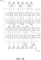
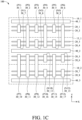
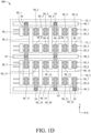
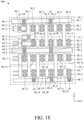
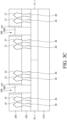
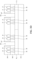
- FIGs. 1A-1E show block diagrams of a layout of features of a semiconductor structure 100 comprising one or more cells in an integrated circuit (IC) according to an embodiment of the invention.
- FIGs. 1A through 1E illustrate features in different levels of the cells, which are consecutively described for clarity.
- the cells may be the standard cells or the memory cells (e.g., SRAM cells) in the IC.
- a P-type well region 15_1 is disposed at the middle of semiconductor structure 100, and two N-type well regions 10_1 and 10_2 are on opposite sides of P-type well region 15_1.
- the fins 20_1 and 20_2 are formed on the N-type well region 10_1, the fins 20_3 through 20_6 are formed on the P-type well region 15_1, and the fins 20_7 and 20_8 are formed on the N-type well region 10_2.
- the fins 20_1 through 20_8 are parallel with the X-direction.
- the gate electrodes 30_1 through 30_17 are arranged parallel with the Y-direction, and the Y-direction is perpendicular to the X-direction.
- the gate electrodes 30_1 through 30_6 form a plurality of PMOS transistors P1 through P6 with the underlying fins 20_1 and 20_2 over the N-type well region 10_1.
- the gate electrodes 30_2, 30_4 and 30_7 through 30_9 form a plurality of NMOS transistors N1 through N6 with the underlying fins 20_3 and 20_4 over the P-type well region 15_1, and the gate electrodes 30_10 through 30_15 form a plurality of NMOS transistors N7 through N12 with the underlying fins 20_5 and 20_6 over the P-type well region 15_1.
- the gate electrodes 30_10 through 30_12, 30_14, 30_16 and 30_17 form a plurality of PMOS transistors P7 through P12 with the underlying fins 20_7 and 20_8 over the N-type well region 10_2.
- the PMOS transistors P1 through P12 and the NMOS transistor N1 through N12 are the dual-fin field effect transistors (FETs). In some embodiments, the PMOS transistors P1 through P12 and the NMOS transistor N1 through N12 are single-fin FETs. In some embodiments, the number of fins under the gate electrodes 30_1 through 30_17 may be the same or different. Furthermore, each gate electrode is capable of connecting to an overlying level through the respective gate contact (also referred to as contact plug) in the IC.
- the gate electrode 30_2 is shared by the PMOS transistor P2 and the NMOS transistor N2.
- the gate electrode 30_4 is shared by the PMOS transistor P4 and the NMOS transistor N4.
- the gate electrode 30_6 is shared by the PMOS transistor P6 and the NMOS transistor N6.
- the gate electrode 30_10 is shared by the PMOS transistor P7 and the NMOS transistor N7.
- the gate electrode 30_11 is shared by the PMOS transistor P8 and the NMOS transistor N8.
- the gate electrode 30_12 is shared by the PMOS transistor P9 and the NMOS transistor N9.
- the gate electrode 30_14 is shared by the PMOS transistor P11 and the NMOS transistor N11.
- the power rails 40_1 through 40_3 are arranged parallel with the X-direction, and formed in the front end of line (FEOL) process of IC fabrication.
- the power rails 40_1 through 40_3 are buried power rails that are embedded in shallow trench isolation (STI) region.
- the power rail 40_1 is formed over the N-type well region 10_1, and is configured to electrically connect a positive power supply line (e.g., a VDD line).
- the power rail 40_3 is formed over the N-type well region 10_2, and is configured to electrically connect a positive power supply line (e.g., a VDD line).
- the power rail 40_2 is formed over the P-type well region 15_1, and is configured to electrically connect a grounding line (e.g., a VSS line).
- the source/drain contacts 50_1 through 50_22 are arranged parallel with the Y-direction. Each source/drain contact is disposed between two adjacent gate electrodes. Furthermore, each source/drain contact (also referred to as "contact") is capable of connecting the source/drain region of corresponding transistor to the overlying level. For example, the source/drain contact 50_1 is disposed between the gate electrodes 30_1 and 30_2, and the source/drain contact 50_2 is disposed between the gate electrodes 30_2 and 30_3. Thus, the gate electrode 30_2 is disposed between the source/drain contacts 50_1 and 50_2. Therefore, the gate region of the PMOS transistor P2 is coupled to the gate electrode 30_2, and the source region and the drain region are coupled to the source/drain contacts 50_1 and 50_2, respectively.
- the source/drain contacts 50_1 and 50_4 are extending above the power rail 40_1 and connecting down to the power rail 40_1 through the lower extension contact 55, thus the source regions of the PMOS transistors P1, P2, P4 and P5 are coupled to the positive power supply line (e.g., a VDD line) through the power rail 40_1 and the corresponding source/drain contact.
- the source region of the PMOS transistor P1 is coupled to the power rail 40_1 through the source/drain contact 50_1.
- the source/drain contacts 50_18, 50_20 and 50_22 are extending above the power rail 40_3 and connecting down to the power rail 40_3 through the lower extension contact 55, thus the source regions of the PMOS transistors P8 through P12 are coupled to the positive power supply line (e.g., a VDD line) through the power rail 40_3 and the corresponding source/drain contact.
- the positive power supply line e.g., a VDD line
- the source/drain contacts 50_7 and 50_10 are extending to cross the power rail 40_2 and connecting down to the power rail 40_2 through the lower extension contact 55, thus the source regions of the NMOS transistors N1, N2, N4, N5, N7, N8, N10 and N11 are coupled to a grounding line (e.g., a VSS line) through the power rail 40_2 and the corresponding source/drain contact.
- a grounding line e.g., a VSS line
- the source region of the NMOS transistor N11 is coupled to the power rail 40_2 through the source/drain contact 50_10.
- the conductive lines 60_1 through 60_6 are arranged parallel with the X-direction. In order to simplify the description, only the conductive lines 60_1 through 60_6 are shown in FIG. 1E , and other conductive lines are omitted.
- the conductive line 60_1 is disposed over the power rail 40_1, and the conductive line 60_1 is coupled to the power rail 40_1 through the vias 65_1 and 65_2 and the corresponding source/drain contacts 50_1 and 50_4. Furthermore, the vias 65_1 and 65_2 are disposed over the lower extension contacts 55.
- the via 65_3 is connected between the gate electrode 30_1 and the conductive line 60_2, which is used to electrically connected the gate region of the PMOS transistor P1 to the conductive line 60_2.
- the via 65_4 is connected between the gate electrode 30_2 and the conductive line 60_3, which is used to electrically connect the gate region of the PMOS transistor P1 and the NMOS transistor N2 to the conductive line 60_3.
- the via 65_5 is connected between the source/drain contact 50_8 and the conductive line 60_4, which is used to electrically connected the drain region of the NMOS transistor N2 to the conductive line 60_4.
- the conductive line 60_5 is disposed over the power rail 40_2, and the conductive line 60_5 is coupled to the power rail 40_2 through the vias 65_6 and 65_7 and the corresponding source/drain contacts 50_7 and 50_10. Furthermore, the vias 65_6 and 65_7 are disposed over the lower extension contacts 55.
- the conductive line 60_6 is disposed over the power rail 40_3, and the conductive line 60_6 is electrically connected to the power rail 40_3 through the via 65_8 and the corresponding source/drain contact 50_20. Furthermore, the via 65_8 is disposed over one of the lower extension contacts 55 on the power rail 40_3. In the embodiment, only the via 65_8 is used to connect the conductive line 60_6 to the power rail 40_3. However, the source/drain contacts 50_18 and 50_22 are connected to the power rail 40_3 through the corresponding lower extension contacts 55. Thus, the source/drain contacts 50_18 and 50_22 are also electrically connected to the conductive line 60_6.
- the conductive line 60_6 and 60_1 are coupled together through the upper conductive lines and the vias between the upper conductive lines over the conductive line 60_6 and 60_1. Due to no via and no conductive line are arranged over the source/drain contacts 50_18 and 50_22, the area over the source/drain contacts 50_18 and 50_22 can be used to provide additional routing area for the signals different from the power lines (e.g., VDD line or VSS line), thereby decreasing layout complexity.
- the power lines e.g., VDD line or VSS line
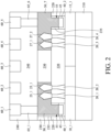
- FIG. 2 shows a cross-sectional view of the semiconductor structure 100 along section line AA-A of FIG. 1E according to an embodiment of the invention.
- the N-type well region 10_1 and the P-type well region 15_1 are formed on a substrate 210.
- the substrate 210 is a Si substrate.
- the fins 20_3 and 20_4 are formed on the P-type well region 15_1.
- the fins 20_3 and 20_4 include an appropriate concentration of P-type dopants (e.g., boron (such as 11B), boron, boron fluorine (BF2), or a combination thereof).
- the fins 20_1 and 20_2 are formed on the N-type well region 10_1.
- the fins 20_1 and 20_2 include an appropriate concentration of n-type dopants (e.g., phosphorous (such as 31P), arsenic, or a combination thereof).
- n-type dopants e.g., phosphorous (such as 31P), arsenic, or a combination thereof.
- the fins 20_1 through 20_4 are separated from each other by the shallow trench isolation (STI) region 220.
- STI shallow trench isolation
- the power rail 40_1 is formed on the N-type well region 10_1, and the power rail 40_2 is formed on the P-type well region 15_1.
- the power rails 40_1 and 40_2 are separated from the fins 20_1 through 20_4 by the STI region 220. Furthermore, the power rails 40_1 and 40_2 are separated from the STI region 220, the N-type well region 10_1 and the P-type well region 15_1 by the barrier layer 45.
- Inter-Layer Dielectric (ILD) layer 230 is formed over the STI region 220.
- the ILD layer 230 may be formed of an oxide such as Phospho-Silicate Glass (PSG), BoroSilicate Glass (BSG), Boron-Doped Phospho-Silicate Glass (BPSG), Tetra Ethyl Ortho Silicate (TEOS) oxide, or the like.
- PSG Phospho-Silicate Glass
- BSG BoroSilicate Glass
- BPSG Boron-Doped Phospho-Silicate Glass
- TEOS Tetra Ethyl Ortho Silicate
- the P-type doping regions 25_1 and 25_2 form the source/drain regions on the fins 20_1 and 20_2
- the N-type doping regions 27_1 and 27_2 form the source/drain regions on the fins 20_3 and 20_4.
- the material of the N-type doping regions 27_1 and 27_2 includes epitaxy profile.
- the epitaxy material is selected from a group consisting of SiP content, SiC content, SiPC, SiAs, Si, or combination. Furthermore, the material of the P-type doping regions 25_1 and 25_2 includes epitaxy profile. The epitaxy material is selected from a group consisting of SiGe content, SiGeC content, Ge-content, or combination.
- the source/drain contact 50_1 is formed around the P-type doping regions 25_1 and 25_2 corresponding to the fins 20_1 and 20_2.
- the source/drain contact 50_1 is electrically connected to the power rail 40_1 through the lower extension contact 55.
- the source/drain contact 50_7 is formed around the N-type doping regions 27_1 and 27_2 corresponding to the fins 20_3 and 20_4.
- the source/drain contact 50_1 is formed over the P-type doping regions 25_1 and 25_2, and the source/drain contact 50_7 is formed over the N-type doping regions 27_1 and 27_2.
- the source/drain contact 50_7 is electrically connected to the power rail 40_2 through the lower extension contact 55.
- the source/drain contacts 50_1 and 50_7 and the corresponding lower extension contacts 55 are separated from the ILD layer 230 and STI region 220 by the blocking layer 235.
- the N-type doping regions 27_1 and 27_2 and the P-type doping regions 25_1 and 25_2 are formed in the ILD layer 230
- the power rails 40_1 and 40_2 are formed in the STI region 220.
- the power rails 40_1 and 40_2 are disposed below the N-type doping regions 27_1 and 27_2 and the P-type doping regions 25_1 and 25_2.
- Inter-metallization dielectric (IMD) layer 240 is formed over the ILD layer 230.
- the vias 65_1 and 65_6 and the conductive lines 60_1 through 60_5 are formed in the IMD layer 240.
- the conductive lines 60_1 through 60_5 are metal lines.
- the source/drain contact 50_1 is electrically connected to the conductive line 60_1 through the via 65_1, thus the conductive line 60_1 over the power rail 40_1 is electrically connected to the power rail 40_1.
- the source/drain contact 50_7 is electrically connected to the conductive line 60_5 through the via 65_6, thus the conductive line 60_5 over the power rail 40_2 is electrically connected to the power rail 40_2.
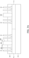
- FIGs. 3A-3H show cross-sectional representations of various stages of forming a semiconductor structure according to an embodiment of the invention.
- a substrate 210 is provided.
- the substrate 102 may be made of silicon or other semiconductor materials.
- the substrate 102 is a wafer.
- the N-type well region 10_1 and the P-type well region 15_1 are formed on the substrate 210.
- the N-type well region 10_1 may be doped with n-type dopants, such as phosphorus (P) or arsenic (As), and the P-type well region 15_1 may be doped with p-type dopants, such as boron or BF2.
- a plurality of fins 20 and a plurality of dummy fins 20D are formed over the N-type well region 10_1 and the P-type well region 15_1. Furthermore, the STI region 220 is formed over the N-type well region 10_1 and the P-type well region 15_1.
- the STI region 220 is an isolation structure that is used to define and electrically isolate the fins 20 and the dummy fins 20D. It should be noted that the dummy fin 20D is wider than the fin 20, i.e., W2>W1. Furthermore, each fin 20 is used to form a transistor in the semiconductor structure, and each dummy fin 20D is used to form a power rail embedded in the STI region 220.
- an ILD planarization is completed on the semiconductor structure.
- the P-type doping regions 25 are formed on the fins 20 over the N-type well region 10_1.
- the N-type doping regions 27 are formed on the fins 20 over the P-type well region 15_1.
- the ILD layer 230 is formed over the STI region 220.
- a spacer 237 is formed between the dummy fin 20D and the ILD layer 230.
- a plurality of openings 250 of the ILD layer 230 are formed above the dummy fins 20D. Furthermore, the spacer 237 and the ILD layer 230 over each dummy fin 20D are removed.
- a wet etching process is performed on the semiconductor structure, so as to remove the dummy fins 20D over the N-type well region 10_1 and the P-type well region 15_1 through the openings 250.
- the trenches 255 are formed over the N-type well region 10_1 and the P-type well region 15_1.
- the barrier layer 45 and the conducting layer 40 are filled up the trenches 255.
- the barrier layer 45 protects the underlying N-type well region 10_1 and P-type well region 15_1 from contacting the conducting material of the conducting layer 40 when the conducting layer 40 is later formed.
- a chemical-mechanical planarization (CMP) is performed on the conducting layer 40, and then the conducting layer 40 in the trench 255 is recessed to a specific height.
- CMP chemical-mechanical planarization
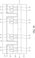
- the remaining conducting layer 40 in the trench 255 forms the power rail (e.g., 40_1 and 40_2 of FIG. 2 ) in the STI region 220.
- the specific height of the power rail 40 is less than that of the fins 20. In some embodiments, the specific height of the power rail 40 is below the P-type doping regions 25_1 and 25_2 and the N-type doping regions 27_1 and 27_2.
- a deposition process is performed to form the hard mask 260 over the power rail 40.
- the subsequent processes before a middle-of-line (MoL) process are performed.
- a replacement metal gate (RMG) is performed on the gate electrodes of the semiconductor structure.
- the source/drain contacts 50a/50b are formed around the P-type doping regions 25 and the N-type doping regions 27.
- each source/drain contact 50a/50b is coupled to the source/drain region of a transistor comprising a dual-fin structure.
- each source/drain contact 50a is connecting down to the adjacent power rail 40 through the corresponding lower extension contact 55.
- the source/drain contact 50a is configured to connect the source region of the PMOS transistor M1 (i.e., the P-type doping region 25 on the right).
- the source region of the PMOS transistor M1 is electrically connected to the power rail 40 over the N-type well region 10_1 through the source/drain contact 50a and the corresponding lower extension contact 55. Furthermore, the N-type well region 10_1 is also electrically connected to the power rail 40. In some embodiments, the power rail 40 over the N-type well region 10_1 and the N-type well region 10_1 are coupled to the positive power supply line (e.g., a VDD line). Similarity, for the NMOS transistor M2 over the P-type well region 15_1, the source/drain contact 50a is configured to connect the source region of the NMOS transistor M2.
- the source region of the NMOS transistor M2 is electrically connected to the power rail 40 over the P-type well region 15_1 through the source/drain contact 50a and the corresponding lower extension contact 55.
- the P-type well region 15_1 is also electrically connected to the power rail 40.
- the power rail 40 over the P-type well region 15_1 and the P-type well region 15_1 are coupled to a grounding line (e.g., a VSS line).
- a semiconductor structure comprising: a shallow trench isolation (STI) region on a well region of a substrate; a plurality of transistors, each comprising: at least one fin formed on the well region, and extending in a first direction; a gate electrode formed on the fin and extending in a second direction that is perpendicular to the first direction; and a doping region formed on the fin; and a power rail formed in the STI region and below the doping regions of the transistors, and extending in the first direction; wherein each of the doping regions is electrically connected to the power rail, so as to form a source region of the respective transistor, and the power rail is electrically connected to the well region of the substrate.
- STI shallow trench isolation
- each of the transistors further comprises: a source contact extending from the doping region to the power rail, wherein the doping region is electrically connected to the power rail through the source contact.
- the transistor is an NMOS transistor, and the power rail is a VSS line.
- the well region is a P-type well region
- the doping region is an N-type doping region
- the transistor is a PMOS transistor, and the power rail is coupled to a VDD line.
- the well region is an N-type well region
- the doping region is a P-type doping region
- integrated circuit comprising: a substrate; an N-type well region on the substrate; a P-type well region on the substrate; a shallow trench isolation (STI) region on the P-type well region and the N-type well region; an interlayer dielectric (ILD) layer over the STI region; a plurality of cells, each comprising: at least one PMOS transistor formed over the N-type well region; and at least one NMOS transistor formed over the P-type well region, wherein the PMOS transistor is separated from the NMOS transistor by the STI region and the LID layer; a VDD line formed in the STI region over the N-type well region and under the LID layer, and electrically connected to a source region of the PMOS transistor; and a VSS line formed in the STI region over the P-type well region and under the LID layer, and electrically connected to a source region of the PMOS transistor.
- STI shallow trench isolation
- ILD interlayer dielectric
- the PMOS transistor comprises: at least one first fin formed on the N-type well region, and extending in a first direction; a first gate electrode formed on the first fin and extending in a second direction that is perpendicular to the first direction; and a P-type doping region on the first fin and separated from the first gate electrode, wherein the VDD line is formed over the N-type well region and below the P-type doping region.
- the NMOS transistor comprises: at least one second fin formed on the P-type well region, and extending in the first direction; a second gate electrode formed on the second fin and extending in the second direction; and an N-type doping region on the second fin and separated from the second gate electrode, wherein the VSS line is formed over the P-type well region and below the N-type doping region.
- the PMOS transistor further comprises: a first source contact extending from the respective P-type doping region to the VDD line, so as to electrically connect the VDD line and the respective P-type doping region.
- the NMOS transistor further comprises: a second source contact extending from the respective N-type doping region to the VSS line, so as to electrically connect the VSS line and the respective N-type doping region.
- the VDD line and VSS line are parallel with the first and second fins, and the cells are arranged in a row between the VDD line and the VSS line.
- the cells comprise standard cells or memory cells.
- a method for manufacturing a semiconductor structure comprising: providing a substrate; forming at least one fin and at least one dummy fin over a well region on the substrate, wherein the fin and the dummy fin are parallel with a first direction, and the dummy fin is wider than the fin; forming a shallow trench isolation (STI) region over the substrate, wherein the fin and the dummy fin are separated from each other by the STI; removing the dummy fin to form a trench in the STI region; and using the trench to form a power rail over the well region.
- STI shallow trench isolation
- the step of using the trench to form the power rail further comprises: filling the trench with conducting material; recessing the conducting material to a specific height; and using the remaining conducting material to form the power rail.
- the method further comprises: forming a doping region on the fin, wherein the power rail is disposed below the doping region.
- the method further comprises: forming a source contact extending from the doping region to the power rail, wherein the doping region is electrically connected to the power rail through the source contact.
- the well region is a P-type well region
- the doping region is an N-type doping region
- the doping region forms a source region of an NMOS transistor corresponding to the fin.
- the well region is an N-type well region
- the doping region is a P-type doping region
- the doping region forms a source region of a PMOS transistor corresponding to the fin.
- the power rail when the well region is a P-type well region, the power rail is a VSS line, and when the well region is an N-type well region, the power rail is a VDD line.
- a greater area over the source/drain contacts that connect to the embedded power rails can be used for routing the signals other than the power rails for layout, thereby decreasing the routing complexity and speed up the design of the IC.
Landscapes
- Metal-Oxide And Bipolar Metal-Oxide Semiconductor Integrated Circuits (AREA)
- Design And Manufacture Of Integrated Circuits (AREA)
- Element Separation (AREA)
- Insulated Gate Type Field-Effect Transistor (AREA)
Applications Claiming Priority (3)
| Application Number | Priority Date | Filing Date | Title |
|---|---|---|---|
| US201762557204P | 2017-09-12 | 2017-09-12 | |
| US16/059,196 US11094594B2 (en) | 2017-09-12 | 2018-08-09 | Semiconductor structure with buried power rail, integrated circuit and method for manufacturing the semiconductor structure |
| EP18191242.9A EP3454366B1 (fr) | 2017-09-12 | 2018-08-28 | Procédé de fabrication d'une structure semi-conductrice à rail d'alimentation enterrée |
Related Parent Applications (1)
| Application Number | Title | Priority Date | Filing Date |
|---|---|---|---|
| EP18191242.9A Division EP3454366B1 (fr) | 2017-09-12 | 2018-08-28 | Procédé de fabrication d'une structure semi-conductrice à rail d'alimentation enterrée |
Publications (2)
| Publication Number | Publication Date |
|---|---|
| EP4379812A2 true EP4379812A2 (fr) | 2024-06-05 |
| EP4379812A3 EP4379812A3 (fr) | 2024-09-04 |
Family
ID=63490217
Family Applications (2)
| Application Number | Title | Priority Date | Filing Date |
|---|---|---|---|
| EP18191242.9A Active EP3454366B1 (fr) | 2017-09-12 | 2018-08-28 | Procédé de fabrication d'une structure semi-conductrice à rail d'alimentation enterrée |
| EP24162760.3A Pending EP4379812A3 (fr) | 2017-09-12 | 2018-08-28 | Structure semi-conductrice avec rail d'alimentation enterré et circuit intégré |
Family Applications Before (1)
| Application Number | Title | Priority Date | Filing Date |
|---|---|---|---|
| EP18191242.9A Active EP3454366B1 (fr) | 2017-09-12 | 2018-08-28 | Procédé de fabrication d'une structure semi-conductrice à rail d'alimentation enterrée |
Country Status (4)
| Country | Link |
|---|---|
| US (3) | US11094594B2 (fr) |
| EP (2) | EP3454366B1 (fr) |
| CN (1) | CN109599400B (fr) |
| TW (1) | TWI710132B (fr) |
Families Citing this family (65)
| Publication number | Priority date | Publication date | Assignee | Title |
|---|---|---|---|---|
| US11094594B2 (en) | 2017-09-12 | 2021-08-17 | Mediatek Inc. | Semiconductor structure with buried power rail, integrated circuit and method for manufacturing the semiconductor structure |
| DE102018127448B4 (de) | 2017-11-30 | 2023-06-22 | Taiwan Semiconductor Manufacturing Co. Ltd. | Metallschienenleiter für nicht-planare Halbleiter-Bauelemente |
| US10700207B2 (en) | 2017-11-30 | 2020-06-30 | Taiwan Semiconductor Manufacturing Company Ltd. | Semiconductor device integrating backside power grid and related integrated circuit and fabrication method |
| JP6934540B2 (ja) * | 2018-02-02 | 2021-09-15 | 東京エレクトロン株式会社 | 半導体装置の製造方法 |
| US11404423B2 (en) * | 2018-04-19 | 2022-08-02 | Taiwan Semiconductor Manufacturing Co., Ltd | Fin-based strap cell structure for improving memory performance |
| US10672665B2 (en) | 2018-09-28 | 2020-06-02 | Taiwan Semiconductor Manufacturing Co., Ltd. | Fin field effect transistor device structure and method for forming the same |
| US11562953B2 (en) * | 2018-10-23 | 2023-01-24 | Taiwan Semiconductor Manufacturing Company, Ltd. | Cell having stacked pick-up region |
| US11030372B2 (en) * | 2018-10-31 | 2021-06-08 | Taiwan Semiconductor Manufacturing Company Ltd. | Method for generating layout diagram including cell having pin patterns and semiconductor device based on same |
| US11093684B2 (en) | 2018-10-31 | 2021-08-17 | Taiwan Semiconductor Manufacturing Company, Ltd. | Power rail with non-linear edge |
| US11063041B2 (en) | 2018-10-31 | 2021-07-13 | Taiwan Semiconductor Manufacturing Co., Ltd. | Integrated circuit device including a power supply line and method of forming the same |
| US11195797B2 (en) | 2019-05-21 | 2021-12-07 | Samsung Electronics Co., Ltd. | Applications of buried power rails |
| JP7268729B2 (ja) | 2019-05-23 | 2023-05-08 | 株式会社ソシオネクスト | 半導体装置 |
| CN113841228B (zh) | 2019-05-23 | 2024-12-27 | 株式会社索思未来 | 半导体装置 |
| US11233008B2 (en) | 2019-06-19 | 2022-01-25 | Samsung Electronics Co., Ltd. | Method of manufacturing an integrated circuit with buried power rail |
| KR102826504B1 (ko) | 2019-07-25 | 2025-06-30 | 삼성전자주식회사 | 반도체 소자 |
| US10950546B1 (en) * | 2019-09-17 | 2021-03-16 | Taiwan Semiconductor Manufacturing Co., Ltd. | Semiconductor device including back side power supply circuit |
| US11114366B2 (en) * | 2019-10-01 | 2021-09-07 | Taiwan Semiconductor Manufacturing Co., Ltd. | Semiconductor structure with buried conductive line and method for forming the same |
| WO2021075353A1 (fr) * | 2019-10-18 | 2021-04-22 | 株式会社ソシオネクスト | Dispositif de circuit intégré à semi-conducteur |
| US11735525B2 (en) * | 2019-10-21 | 2023-08-22 | Tokyo Electron Limited | Power delivery network for CFET with buried power rails |
| CN112786535B (zh) * | 2019-11-05 | 2024-07-16 | 中芯国际集成电路制造(上海)有限公司 | 半导体结构的形成方法 |
| EP3836196B1 (fr) | 2019-12-13 | 2023-04-26 | Imec VZW | Contacts auto-alignés pour dispositifs à transistor à effet de champ à nanofeuilles |
| EP3840054B1 (fr) * | 2019-12-20 | 2023-07-05 | Imec VZW | Contacts auto-alignés pour dispositifs de transistor à effet de champ à nanosheet et forksheet à parois |
| US11646317B2 (en) | 2020-02-27 | 2023-05-09 | Taiwan Semiconductor Manufacturing Company, Ltd. | Integrated circuit device, method, and system |
| CN113314529B (zh) * | 2020-02-27 | 2025-12-19 | 台湾积体电路制造股份有限公司 | 集成电路装置及其形成方法、集成电路的系统 |
| US11145550B2 (en) * | 2020-03-05 | 2021-10-12 | International Business Machines Corporation | Dummy fin template to form a self-aligned metal contact for output of vertical transport field effect transistor |
| US11600707B2 (en) * | 2020-05-12 | 2023-03-07 | Micron Technology, Inc. | Methods of forming conductive pipes between neighboring features, and integrated assemblies having conductive pipes between neighboring features |
| DE102021107950A1 (de) * | 2020-05-28 | 2021-12-02 | Taiwan Semiconductor Manufacturing Co., Ltd. | Verfahren zum fertigen von halbleiterbauelementen mit unterschiedlichen architekturen und damit gefertigte halbleiterbauelemente |
| WO2021259479A1 (fr) * | 2020-06-25 | 2021-12-30 | Huawei Technologies Co., Ltd. | Dispositif à semi-conducteur, puce semi-conductrice et procédé pour la fabrication d'un dispositif à semi-conducteur |
| US11637069B2 (en) * | 2020-08-31 | 2023-04-25 | Taiwan Semiconductor Manufacturing Company, Ltd. | Semiconductor device with V2V rail and methods of making same |
| CN114256142B (zh) * | 2020-09-24 | 2026-02-27 | 中芯国际集成电路制造(上海)有限公司 | 半导体结构及其形成方法 |
| CN114256140B (zh) * | 2020-09-24 | 2026-03-03 | 中芯国际集成电路制造(上海)有限公司 | 半导体结构及其形成方法 |
| US11908910B2 (en) * | 2020-10-27 | 2024-02-20 | Taiwan Semiconductor Manufacturing Company, Ltd. | Semiconductor device having embedded conductive line and method of fabricating thereof |
| US11521927B2 (en) | 2020-11-10 | 2022-12-06 | International Business Machines Corporation | Buried power rail for scaled vertical transport field effect transistor |
| US11769728B2 (en) | 2020-11-13 | 2023-09-26 | Samsung Electronics Co., Ltd. | Backside power distribution network semiconductor package and method of manufacturing the same |
| US12094822B2 (en) | 2020-11-17 | 2024-09-17 | Intel Corporation | Buried power rails with self-aligned vias to trench contacts |
| JP7799195B2 (ja) * | 2020-12-25 | 2026-01-15 | 株式会社ソシオネクスト | 半導体集積回路装置 |
| US11621332B2 (en) | 2021-01-14 | 2023-04-04 | International Business Machines Corporation | Wraparound contact to a buried power rail |
| KR102777095B1 (ko) | 2021-02-18 | 2025-03-05 | 삼성전자주식회사 | 반도체 장치 및 그 제조 방법 |
| US12327791B2 (en) * | 2021-03-23 | 2025-06-10 | Intel Corporation | Integrated circuit structures with gate cuts above buried power rails |
| US20220336355A1 (en) * | 2021-04-19 | 2022-10-20 | Samsung Electronics Co., Ltd. | Thermal budget enhanced buried power rail and method of manufacturing the same |
| US11810919B2 (en) * | 2021-06-17 | 2023-11-07 | Taiwan Semiconductor Manufacturing Company, Ltd. | Semiconductor device structure with conductive via structure and method for forming the same |
| US11855005B2 (en) * | 2021-06-21 | 2023-12-26 | Globalfoundries U.S. Inc. | Crackstop with embedded passive radio frequency noise suppressor and method |
| US12237233B2 (en) | 2021-07-06 | 2025-02-25 | Taiwan Semiconductor Manufacturing Co., Ltd. | Backside power rail for physical failure analysis (PFA) |
| US12283587B2 (en) * | 2021-07-09 | 2025-04-22 | Taiwan Semiconductor Manufacturing Company, Ltd. | Integrated circuit and method of forming the same |
| CN115602631A (zh) * | 2021-07-09 | 2023-01-13 | 中芯国际集成电路制造(上海)有限公司(Cn) | 半导体结构及其形成方法 |
| US12002874B2 (en) | 2021-07-26 | 2024-06-04 | International Business Machines Corporation | Buried power rail contact |
| US11804436B2 (en) | 2021-09-03 | 2023-10-31 | International Business Machines Corporation | Self-aligned buried power rail cap for semiconductor devices |
| US12046643B2 (en) * | 2021-09-20 | 2024-07-23 | International Business Machines Corporation | Semiconductor structures with power rail disposed under active gate |
| US12317582B2 (en) | 2021-09-22 | 2025-05-27 | Samsung Electronics Co., Ltd. | Integrated circuit devices including a metal resistor and methods of forming the same |
| US20230117743A1 (en) * | 2021-10-20 | 2023-04-20 | International Business Machines Corporation | Self-aligned buried power rail formation for semiconductor devices |
| US12426338B2 (en) | 2021-10-27 | 2025-09-23 | International Business Machines Corporation | Buried power rail with robust connection to a wrap around contact |
| US12406930B2 (en) | 2021-10-28 | 2025-09-02 | International Business Machines Corporation | Structure containing a via-to-buried power rail contact structure or a via-to-backside power rail contact structure |
| US20230154783A1 (en) * | 2021-11-16 | 2023-05-18 | International Business Machines Corporation | Replacement buried power rail |
| US20230187510A1 (en) * | 2021-12-15 | 2023-06-15 | International Business Machines Corporation | Angled via for tip to tip margin improvement |
| EP4199052B1 (fr) * | 2021-12-17 | 2024-08-21 | IMEC vzw | Schéma de métallisation pour un circuit intégré |
| CN116344449B (zh) * | 2021-12-22 | 2025-08-19 | 中芯国际集成电路制造(上海)有限公司 | 半导体结构及其形成方法 |
| US12616019B2 (en) | 2022-06-10 | 2026-04-28 | International Business Machines Corporation | Via connection to backside power delivery network |
| US12272648B2 (en) | 2022-06-15 | 2025-04-08 | International Business Machines Corporation | Semiconductor device having a backside power rail |
| US12557633B2 (en) | 2022-06-17 | 2026-02-17 | International Business Machines Corporation | Multiple critical dimension power rail |
| US20240079239A1 (en) * | 2022-09-07 | 2024-03-07 | Taiwan Semiconductor Manufacturing Co., Ltd. | Etch Stop Region for Semiconductor Device Substrate Thinning |
| US20240105788A1 (en) * | 2022-09-27 | 2024-03-28 | International Business Machines Corporation | Local interconnect at backside to enable flexible routing across different cell |
| US12150393B2 (en) | 2022-09-30 | 2024-11-19 | International Business Machines Corporation | Heater for phase change material memory cell |
| US12451422B2 (en) | 2022-10-11 | 2025-10-21 | Samsung Electronics Co., Ltd. | Semiconductor device |
| US20240169137A1 (en) * | 2022-11-18 | 2024-05-23 | SamsungElectronicsCo.,Ltd. | Integrated circuit including standard cells and method of designing the same |
| US20240332183A1 (en) * | 2023-03-31 | 2024-10-03 | Adeia Semiconductor Bonding Technologies, Inc. | Direct bonding on buried power rails |
Family Cites Families (19)
| Publication number | Priority date | Publication date | Assignee | Title |
|---|---|---|---|---|
| US6583045B1 (en) | 2001-11-16 | 2003-06-24 | Taiwan Semiconductor Manufacturing Company | Chip design with power rails under transistors |
| JP2008153435A (ja) * | 2006-12-18 | 2008-07-03 | Matsushita Electric Ind Co Ltd | 半導体集積回路 |
| US8980719B2 (en) * | 2010-04-28 | 2015-03-17 | Taiwan Semiconductor Manufacturing Company, Ltd. | Methods for doping fin field-effect transistors |
| US8890260B2 (en) * | 2009-09-04 | 2014-11-18 | Taiwan Semiconductor Manufacturing Company, Ltd. | Polysilicon design for replacement gate technology |
| US8293602B2 (en) * | 2010-11-19 | 2012-10-23 | Micron Technology, Inc. | Method of fabricating a finFET having cross-hair cells |
| US8507957B2 (en) | 2011-05-02 | 2013-08-13 | Taiwan Semiconductor Manufacturing Company, Ltd. | Integrated circuit layouts with power rails under bottom metal layer |
| KR20160040577A (ko) * | 2013-08-06 | 2016-04-14 | 르네사스 일렉트로닉스 가부시키가이샤 | 반도체 집적 회로 장치 |
| US20150145041A1 (en) * | 2013-11-22 | 2015-05-28 | International Business Machines Corporation | Substrate local interconnect integration with finfets |
| US9263340B2 (en) | 2014-05-02 | 2016-02-16 | Globalfoundries Inc. | Methods for removing selected fins that are formed for finFET semiconductor devices |
| JP6449082B2 (ja) * | 2014-08-18 | 2019-01-09 | ルネサスエレクトロニクス株式会社 | 半導体装置 |
| KR102282980B1 (ko) * | 2015-01-05 | 2021-07-29 | 삼성전자주식회사 | 실리사이드를 갖는 반도체 소자 및 그 형성 방법 |
| KR102366976B1 (ko) * | 2015-05-04 | 2022-02-24 | 삼성전자주식회사 | 콘택 플러그를 갖는 반도체 소자 및 그 형성 방법 |
| EP3139405B1 (fr) * | 2015-09-01 | 2021-08-11 | IMEC vzw | Interconnexion enterrée de circuits à semi-conducteurs |
| EP3324436B1 (fr) | 2016-11-21 | 2020-08-05 | IMEC vzw | Puce de circuit intégré avec réseau de distribution électrique sur la face arrière de la puce |
| US10170413B2 (en) * | 2016-11-28 | 2019-01-01 | Taiwan Semiconductor Manufacturing Co., Ltd. | Semiconductor device having buried metal line and fabrication method of the same |
| US10475692B2 (en) * | 2017-04-07 | 2019-11-12 | Globalfoundries Inc. | Self aligned buried power rail |
| US10290635B2 (en) * | 2017-07-26 | 2019-05-14 | Taiwan Semiconductor Manufacturing Co., Ltd. | Buried interconnect conductor |
| US10446555B2 (en) * | 2017-08-31 | 2019-10-15 | Taiwan Semiconductor Manufacturing Company, Ltd. | Buried metal track and methods forming same |
| US11094594B2 (en) | 2017-09-12 | 2021-08-17 | Mediatek Inc. | Semiconductor structure with buried power rail, integrated circuit and method for manufacturing the semiconductor structure |
-
2018
- 2018-08-09 US US16/059,196 patent/US11094594B2/en active Active
- 2018-08-28 EP EP18191242.9A patent/EP3454366B1/fr active Active
- 2018-08-28 EP EP24162760.3A patent/EP4379812A3/fr active Pending
- 2018-09-11 CN CN201811058232.7A patent/CN109599400B/zh active Active
- 2018-09-12 TW TW107132034A patent/TWI710132B/zh active
-
2021
- 2021-07-07 US US17/369,633 patent/US12165927B2/en active Active
-
2024
- 2024-12-06 US US18/971,358 patent/US20250098283A1/en active Pending
Also Published As
| Publication number | Publication date |
|---|---|
| EP3454366B1 (fr) | 2024-03-13 |
| TWI710132B (zh) | 2020-11-11 |
| US12165927B2 (en) | 2024-12-10 |
| CN109599400B (zh) | 2021-06-08 |
| US20210335675A1 (en) | 2021-10-28 |
| US20190080969A1 (en) | 2019-03-14 |
| EP4379812A3 (fr) | 2024-09-04 |
| EP3454366A1 (fr) | 2019-03-13 |
| US20250098283A1 (en) | 2025-03-20 |
| TW201914011A (zh) | 2019-04-01 |
| US11094594B2 (en) | 2021-08-17 |
| CN109599400A (zh) | 2019-04-09 |
Similar Documents
| Publication | Publication Date | Title |
|---|---|---|
| US12165927B2 (en) | Semiconductor structure with buried power rail, integrated circuit and method for manufacturing the semiconductor structure | |
| KR102780325B1 (ko) | 후면 전력 전달로의 대체 매설 전력 레일 | |
| US11088166B2 (en) | 3D NAND memory device and method of forming the same | |
| CN111801798B (zh) | 三维存储器件 | |
| CN109979888B (zh) | 半导体结构 | |
| CN107039525B (zh) | 用于高功率电迁移的通孔轨解决方案 | |
| KR102320047B1 (ko) | 집적회로 소자 및 그 제조 방법 | |
| US8975712B2 (en) | Densely packed standard cells for integrated circuit products, and methods of making same | |
| CN100466263C (zh) | 深沟槽去耦电容器器件及其制造方法 | |
| US9209192B2 (en) | Semiconductor device and method of fabricating the same | |
| US11626516B2 (en) | Integrated circuitry including vertical channel structure and layout method of the same | |
| US10043571B1 (en) | SRAM structure | |
| US10784168B2 (en) | Dummy MOL removal for performance enhancement | |
| KR20140026571A (ko) | 6f2 dram 셀 | |
| US6974987B2 (en) | Semiconductor device | |
| TW201630158A (zh) | 半導體積體電路 | |
| US20130193516A1 (en) | Sram integrated circuits and methods for their fabrication | |
| US20250335686A1 (en) | Cfet device optimization by multiple cell height placement | |
| US20240120257A1 (en) | Layer-By-Layer Formation Of Through-Substrate Via | |
| JP5905752B2 (ja) | 半導体装置及びその製造方法 | |
| KR101167202B1 (ko) | 모스 트랜지스터 및 시모스 인버터 및 그 제조방법 | |
| CN118201353A (zh) | 集成电路装置 | |
| CN121865607A (zh) | 静态随机存取存储器的布局图案以及其制作方法 |
Legal Events
| Date | Code | Title | Description |
|---|---|---|---|
| PUAI | Public reference made under article 153(3) epc to a published international application that has entered the european phase |
Free format text: ORIGINAL CODE: 0009012 |
|
| STAA | Information on the status of an ep patent application or granted ep patent |
Free format text: STATUS: THE APPLICATION HAS BEEN PUBLISHED |
|
| AC | Divisional application: reference to earlier application |
Ref document number: 3454366 Country of ref document: EP Kind code of ref document: P |
|
| AK | Designated contracting states |
Kind code of ref document: A2 Designated state(s): AL AT BE BG CH CY CZ DE DK EE ES FI FR GB GR HR HU IE IS IT LI LT LU LV MC MK MT NL NO PL PT RO RS SE SI SK SM TR |
|
| PUAL | Search report despatched |
Free format text: ORIGINAL CODE: 0009013 |
|
| AK | Designated contracting states |
Kind code of ref document: A3 Designated state(s): AL AT BE BG CH CY CZ DE DK EE ES FI FR GB GR HR HU IE IS IT LI LT LU LV MC MK MT NL NO PL PT RO RS SE SI SK SM TR |
|
| RIC1 | Information provided on ipc code assigned before grant |
Ipc: H01L 21/74 20060101ALI20240730BHEP Ipc: H01L 23/528 20060101ALI20240730BHEP Ipc: H01L 21/768 20060101ALI20240730BHEP Ipc: H01L 27/092 20060101ALI20240730BHEP Ipc: H01L 21/8238 20060101ALI20240730BHEP Ipc: H01L 29/78 20060101AFI20240730BHEP |
|
| STAA | Information on the status of an ep patent application or granted ep patent |
Free format text: STATUS: REQUEST FOR EXAMINATION WAS MADE |
|
| 17P | Request for examination filed |
Effective date: 20250212 |