EP4386864A1 - Solarzelle und fotovoltaisches modul - Google Patents
Solarzelle und fotovoltaisches modul Download PDFInfo
- Publication number
- EP4386864A1 EP4386864A1 EP23196106.1A EP23196106A EP4386864A1 EP 4386864 A1 EP4386864 A1 EP 4386864A1 EP 23196106 A EP23196106 A EP 23196106A EP 4386864 A1 EP4386864 A1 EP 4386864A1
- Authority
- EP
- European Patent Office
- Prior art keywords
- region
- conductive layer
- doped conductive
- solar cell
- layer
- Prior art date
- Legal status (The legal status is an assumption and is not a legal conclusion. Google has not performed a legal analysis and makes no representation as to the accuracy of the status listed.)
- Granted
Links
Images


Classifications
-
- H—ELECTRICITY
- H10—SEMICONDUCTOR DEVICES; ELECTRIC SOLID-STATE DEVICES NOT OTHERWISE PROVIDED FOR
- H10F—INORGANIC SEMICONDUCTOR DEVICES SENSITIVE TO INFRARED RADIATION, LIGHT, ELECTROMAGNETIC RADIATION OF SHORTER WAVELENGTH OR CORPUSCULAR RADIATION
- H10F10/00—Individual photovoltaic cells, e.g. solar cells
- H10F10/10—Individual photovoltaic cells, e.g. solar cells having potential barriers
- H10F10/16—Photovoltaic cells having only PN heterojunction potential barriers
- H10F10/164—Photovoltaic cells having only PN heterojunction potential barriers comprising heterojunctions with Group IV materials, e.g. ITO/Si or GaAs/SiGe photovoltaic cells
- H10F10/165—Photovoltaic cells having only PN heterojunction potential barriers comprising heterojunctions with Group IV materials, e.g. ITO/Si or GaAs/SiGe photovoltaic cells the heterojunctions being Group IV-IV heterojunctions, e.g. Si/Ge, SiGe/Si or Si/SiC photovoltaic cells
- H10F10/166—Photovoltaic cells having only PN heterojunction potential barriers comprising heterojunctions with Group IV materials, e.g. ITO/Si or GaAs/SiGe photovoltaic cells the heterojunctions being Group IV-IV heterojunctions, e.g. Si/Ge, SiGe/Si or Si/SiC photovoltaic cells the Group IV-IV heterojunctions being heterojunctions of crystalline and amorphous materials, e.g. silicon heterojunction [SHJ] photovoltaic cells
-
- H—ELECTRICITY
- H10—SEMICONDUCTOR DEVICES; ELECTRIC SOLID-STATE DEVICES NOT OTHERWISE PROVIDED FOR
- H10F—INORGANIC SEMICONDUCTOR DEVICES SENSITIVE TO INFRARED RADIATION, LIGHT, ELECTROMAGNETIC RADIATION OF SHORTER WAVELENGTH OR CORPUSCULAR RADIATION
- H10F77/00—Constructional details of devices covered by this subclass
- H10F77/10—Semiconductor bodies
- H10F77/14—Shape of semiconductor bodies; Shapes, relative sizes or dispositions of semiconductor regions within semiconductor bodies
-
- H—ELECTRICITY
- H10—SEMICONDUCTOR DEVICES; ELECTRIC SOLID-STATE DEVICES NOT OTHERWISE PROVIDED FOR
- H10F—INORGANIC SEMICONDUCTOR DEVICES SENSITIVE TO INFRARED RADIATION, LIGHT, ELECTROMAGNETIC RADIATION OF SHORTER WAVELENGTH OR CORPUSCULAR RADIATION
- H10F10/00—Individual photovoltaic cells, e.g. solar cells
- H10F10/10—Individual photovoltaic cells, e.g. solar cells having potential barriers
- H10F10/14—Photovoltaic cells having only PN homojunction potential barriers
-
- H—ELECTRICITY
- H10—SEMICONDUCTOR DEVICES; ELECTRIC SOLID-STATE DEVICES NOT OTHERWISE PROVIDED FOR
- H10F—INORGANIC SEMICONDUCTOR DEVICES SENSITIVE TO INFRARED RADIATION, LIGHT, ELECTROMAGNETIC RADIATION OF SHORTER WAVELENGTH OR CORPUSCULAR RADIATION
- H10F10/00—Individual photovoltaic cells, e.g. solar cells
- H10F10/10—Individual photovoltaic cells, e.g. solar cells having potential barriers
- H10F10/17—Photovoltaic cells having only PIN junction potential barriers
-
- H—ELECTRICITY
- H10—SEMICONDUCTOR DEVICES; ELECTRIC SOLID-STATE DEVICES NOT OTHERWISE PROVIDED FOR
- H10F—INORGANIC SEMICONDUCTOR DEVICES SENSITIVE TO INFRARED RADIATION, LIGHT, ELECTROMAGNETIC RADIATION OF SHORTER WAVELENGTH OR CORPUSCULAR RADIATION
- H10F71/00—Manufacture or treatment of devices covered by this subclass
- H10F71/121—The active layers comprising only Group IV materials
-
- H—ELECTRICITY
- H10—SEMICONDUCTOR DEVICES; ELECTRIC SOLID-STATE DEVICES NOT OTHERWISE PROVIDED FOR
- H10F—INORGANIC SEMICONDUCTOR DEVICES SENSITIVE TO INFRARED RADIATION, LIGHT, ELECTROMAGNETIC RADIATION OF SHORTER WAVELENGTH OR CORPUSCULAR RADIATION
- H10F77/00—Constructional details of devices covered by this subclass
- H10F77/20—Electrodes
- H10F77/206—Electrodes for devices having potential barriers
- H10F77/211—Electrodes for devices having potential barriers for photovoltaic cells
-
- H—ELECTRICITY
- H10—SEMICONDUCTOR DEVICES; ELECTRIC SOLID-STATE DEVICES NOT OTHERWISE PROVIDED FOR
- H10F—INORGANIC SEMICONDUCTOR DEVICES SENSITIVE TO INFRARED RADIATION, LIGHT, ELECTROMAGNETIC RADIATION OF SHORTER WAVELENGTH OR CORPUSCULAR RADIATION
- H10F77/00—Constructional details of devices covered by this subclass
- H10F77/30—Coatings
- H10F77/306—Coatings for devices having potential barriers
- H10F77/311—Coatings for devices having potential barriers for photovoltaic cells
Definitions
- the present disclosure relates to the photovoltaic technical field, and in particular, to a solar cell and a photovoltaic module.
- a solar cell can directly convert solar radiation energy into electrical energy, based on a photovoltaic effect of crystalline silicon.
- photons of sunlight are absorbed by the crystalline silicon, electron-hole pairs may be generated.
- the electrons and holes when arriving at a p-n junction composed of p-type crystalline silicon and n-type crystalline silicon, are respectively separated to two sides of the p-n junction by a junction electric field.
- a photocurrent current is generated, and electric energy is outputted.
- solar cells are generally connected in series/parallel and then packaged together to form a photovoltaic module.
- the solar cell further includes doped polysilicon, and the doped polysilicon may absorb light, which reduce the photoelectric conversion efficiency of the solar cell.
- the doped polysilicon may absorb light, which reduce the photoelectric conversion efficiency of the solar cell.
- a thickness of the doped polysilicon is generally reduced.
- the thinner doped polysilicon has a large lateral transport resistance and an increased carrier recombination probability, so the reduction in the thickness of the doped polysilicon reduces the photoelectric conversion efficiency of the solar cell.
- Embodiments of the present disclosure provide a solar cell and a photovoltaic module.
- the solar cell has a reduced transverse resistance and increased recombination due to a thinner first doped conductive layer, thereby improving photoelectric conversion efficiency of the solar cell.
- the solar cell includes a body and a first electrode.
- the body has a first region and a second region. Along a thickness direction of the solar cell, at least part of the first region covers the first electrode.
- the second region is a region of the body other than the first region.
- the body includes a substrate, a first tunneling layer, a first doped conductive layer, and a second doped conductive layer.
- the first tunneling layer is arranged on a side of the substrate, and the first tunneling layer has a greater thickness in the first region than in the second region.
- the first doped conductive layer is arranged on a surface of the first tunneling layer away from the substrate, and the first electrode is electrically connected to the first doped conductive layer.
- the second doped conductive layer is located on a side of the substrate adjacent to the first tunneling layer, and the second doped conductive layer has a less thickness in the first region than in the second region.
- the first tunneling layer in the first region protrudes towards the first doped conductive layer with respect to the first tunneling layer in the second region
- the second doped conductive layer in the second region protrudes towards the substrate with respect to the second doped conductive layer in the first region
- the first tunneling layer in the first region protrudes towards the substrate with respect to the first tunneling layer in the second region
- the second doped conductive layer in the second region protrudes towards the first doped conductive layer with respect to the second doped conductive layer in the first region
- doping concentration of a dopant element in the first region is less than that in the second region.
- the doping concentration c1 of the dopant element in the first region of the second doped conductive layer satisfies: 1 ⁇ 10 18 atoms/cm 3 ⁇ c1 ⁇ 1 ⁇ 10 20 atoms/cm 3 .
- the doping concentration c2 of the dopant element in the second region of the second doped conductive layer satisfies: 1 ⁇ 10 19 atoms/cm 3 ⁇ c2 ⁇ 2 ⁇ 10 20 atoms/cm 3 .
- a thickness H11 of the first tunneling layer in the first region satisfies: 1 nm ⁇ H11 ⁇ 2.5 nm.
- a thickness H12 of the first tunneling layer in the second region satisfies: 0.5 nm ⁇ H12 ⁇ 2 nm.
- a thickness H21 of the second doped conductive layer in the first region satisfies: 0 ⁇ m ⁇ H21 ⁇ 0.5 ⁇ m.
- a thickness H22 of the second doped conductive layer in the second region satisfies: 0 ⁇ m ⁇ H22 ⁇ 1 ⁇ m.
- the first region is arranged alternately with the second region along a width direction of the solar cell.
- a width D1 of the first region satisfies: 10 ⁇ m ⁇ D1 ⁇ 200 ⁇ m.
- a ratio of a width D2 of the first electrode to a width D1 of the first region satisfies: 0.3 ⁇ D2/D1 ⁇ 1.
- the body further includes an emitter arranged on a surface of the substrate away from the first tunneling layer, and the solar cell further includes a second electrode electrically connected to the emitter.
- the body further includes a first passivation layer and a second passivation layer, the first passivation layer is arranged on a side of the first doped conductive layer away from the substrate, and the second passivation layer is arranged on a side of the emitter away from the substrate.
- the body further includes: a second tunneling layer, a third doped conductive layer, and a fourth doped conductive layer.
- the second tunneling layer is arranged on a side of the substrate away from the first tunneling layer, and the second tunneling layer has a greater thickness in the first region than in the second region.
- the third doped conductive layer is arranged on a surface of the second tunneling layer away from the substrate, and the fourth doped conductive layer is located on a side of the substrate close to the second tunneling layer, and the fourth doped conductive layer has a less thickness in the first region than in the second region.
- the solar cell further includes a third electrode electrically connected to the third doped conductive layer.
- the body further includes a first passivation layer and a third passivation layer, the first passivation layer is arranged on a side of the first doped conductive layer away from the substrate, and the third passivation layer is arranged on a side of the third doped conductive layer away from the substrate.
- the photovoltaic module includes: a solar cell string, an encapsulation layer, and a cover plate.
- the solar cell string includes a plurality of solar cells connected to one another, the encapsulation layer covers a surface of the solar cell string, and the cover plate covers a surface of the packaging layer away from the solar cell string.
- the solar cell includes a body and a first electrode.
- the body has a first region and a second region. Along a thickness direction of the solar cell, at least part of the first region covers the first electrode.
- the second region is a region of the body other than the first region.
- the body includes a substrate, a first tunneling layer, a first doped conductive layer, and a second doped conductive layer.
- the first tunneling layer is arranged on a side of the substrate, and the first tunneling layer has a greater thickness in the first region than in the second region.
- the first doped conductive layer is arranged on a surface of the first tunneling layer away from the substrate, and the first electrode is electrically connected to the first doped conductive layer.
- the second doped conductive layer is located on a side of the substrate adjacent to the first tunneling layer, and the second doped conductive layer has a less thickness in the first region than in the second region.
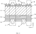
- the solar cell includes a body and a first electrode 21.
- the body has a first region I and a second region II.
- the thickness direction X of the solar cell is a direction perpendicular to the solar cell.
- the second region II is a region of the body other than the first region I.
- the body includes: a substrate 11, a first tunneling layer 12, a first doped conductive layer 13, and a second doped conductive layer 14.
- the first tunneling layer 12 is arranged on a side of the substrate 11, and a thickness of the first tunneling layer 12 in the first region I is greater than that in the second region II.
- the first doped conductive layer 13 is arranged on a surface of the first tunneling layer 12 away from the substrate 11, and the first electrode 21 is electrically connected to the first doped conductive layer 13. As shown in FIG. 1 , the first electrode 21 is in contact with the first doped conductive layer 13.
- the second doped conductive layer 14 is located on a side of the substrate 11 adjacent to the first tunneling layer 12, and a thickness of the second doped conductive layer 14 in the first region I is less than that in the second region II.
- the first tunneling layer 12 is a tunneling layer for majority carriers, and at the same time chemically passivates the substrate 11 to reduce interface states.
- the first doped conductive layer 13 can form energy band bending, realize selective transport of the carriers, and reduce recombination losses of the carriers.
- the first electrode 21 is electrically connected to the first doped conductive layer 13, and is not in contact with the first tunneling layer 12, thereby maintaining good interface passivation.
- a small part of the dopant element in the first doped conductive layer 13 may enter the substrate 11 by passing through the first tunneling layer 12, and form the second doped conductive layer 14 on a surface of the substrate 11. Since the thickness of the first tunneling layer 12 in the first region I is different from that in the second region II, the thickness of the second doped conductive layer 14 on the surface of the substrate 11 formed by the dopant element from the first doped conductive layer 13 is different.
- the thickness of the first tunneling layer 12 in the first region I is greater than that in the second region II, so that the thickness of the second doped conductive layer 14 in the first region I is less than that in the second region II.
- the first electrode 21 extends into the first doped conductive layer 13, which damages a structure of the first doped conductive layer 13 and increases recombination of carriers.
- a thicker first tunneling layer 12 is arranged on a side of the first electrode 21 adjacent to the substrate 11, which can improve a passivation effect of the first region, reduce the thickness of the second doped conductive layer 14, reduce the recombination of the carriers, and improve the photoelectric conversion efficiency of the solar cell.
- a thinner first tunneling layer 12 improves transport capability of the carriers from the substrate 11 to the first doped conductive layer 13, and makes the second doped conductive layer 14 thicker.
- the sheet resistance of the second doped conductive layer 14 is reduced, the transverse transport capability of the carriers in the second doped conductive layer 14 is improved, and the photoelectric conversion efficiency of the solar cell is improved.
- the substrate 11 may be a crystalline semiconductor (e.g., crystalline silicon) containing a dopant element.
- the dopant element may be an N-type dopant element such as a Group V element including phosphorus (P), arsenic (As), bismuth (Bi), and antimony (Sb), or a P-type dopant element such as a Group III element including boron (B), aluminum (Al), gallium (Ga), and indium (In).
- the first tunneling layer 12 is a silicon oxide layer (SiO x ), with a thickness ranging from 0.5 nm to 2.5 nm.
- the thickness of the first tunneling layer 12 may be, for example, 0.5 nm, 1 nm, 1.5 nm, 2 nm, 2.5 nm, or the like.
- a material of the first electrode 21 includes at least one conductive metal material such as silver, aluminum, copper, nickel, or the like.
- the photoelectric conversion efficiency of the solar cell may include a photoelectric conversion efficiency at a front surface of the solar cell and a photoelectric conversion efficiency at a back surface of the solar cell.
- a bifaciality of the solar cell may refer to a ratio of the photoelectric conversion efficiency at the back surface of the solar cell to the photoelectric conversion efficiency at the front surface of the solar cell. If the first doped conductive layer 13 is thicker, the first doped conductive layer 13 absorbs more light energy, and fewer light is received by the substrate 11, which affects the photoelectric conversion efficiency at the back surface of the solar cell and reduces the bifaciality of the solar cell. At the same time, if the first doped conductive layer 13 is thicker, the front efficiency of the solar cell can also be reduced.
- the first tunneling layer 12 in the first region I protrudes towards the first doped conductive layer 13 with respect to the first tunneling layer 12 in the second region II
- the second doped conductive layer 14 in the second region II protrudes towards the substrate 11 with respect to the second doped conductive layer 14 in the first region I.
- the first tunneling layer 12 in the first region I protrudes towards the substrate 11 with respect to the first tunneling layer 12 in the second region II
- the second doped conductive layer 14 in the second region II protrudes towards the first doped conductive layer 13 with respect to the second doped conductive layer 14 in the first region I.
- the first tunneling layer 12 in the first region I protrudes towards the first doped conductive layer 13 with respect to the first tunneling layer 12 in the second region II, so that the second doped conductive layer 14 in the second region II protrudes towards the substrate 11 with respect to the second doped conductive layer 14 in the first region I. That is, an interface between the first tunneling layer 12 and the second doped conductive layer 14 is a substantially flat plane.
- the first tunneling layer 12 in the first region I protrudes towards the substrate 11 with respect to the first tunneling layer 12 in the second region II, so that the second doped conductive layer 14 in the second region II protrudes towards the first doped conductive layer 13 with respect to the second doped conductive layer 14 in the first region I. That is, an interface between the first tunneling layer 12 and the first doped conductive layer 13 is a substantially flat plane, and a surface of the second doped conductive layer 14 away from the first tunneling layer 12 is a substantially flat plane.
- a doping concentration of a dopant element in the first region I is less than that in the second region II.
- the doping concentration of the dopant element in the second doped conductive layer 14 in the first region I is smaller, recombination of the carriers caused by the influence of the first electrode 21 on the body can be reduced. If the doping concentration of the dopant element in the second doped conductive layer 14 in the second region II is greater, resistance of the body can be reduced, and the transverse transport capability of the carriers can be improved, thereby improving the photoelectric conversion efficiency of the solar cell.
- the dopant element in the second doped conductive layer 14 is from the first doped conductive layer 13, so the dopant element in the second doped conductive layer 14 is the same as the dopant element in the first doped conductive layer 13.
- the first doped conductive layer 13 may be amorphous silicon, microcrystalline silicon, polycrystalline silicon, or the like including the dopant element.
- the dopant element may be an N-type dopant element such as a Group V element including P, As, Bi, and Sb, or a P-type dopant element such as a Group III element including B, Al, Ga, and In.
- the first doped conductive layer 13 and the substrate 11 are doped with a same type of dopant element.
- the doping concentration c1 of the dopant element of the second doped conductive layer 14 in the first region I satisfies: 1 ⁇ 10 18 atoms/cm 3 ⁇ c1 ⁇ 1 ⁇ 10 20 atoms/cm 3 .
- the doping concentration c1 may be 1 ⁇ 10 18 atoms/cm 3 , 0.5 ⁇ 10 19 atoms/cm 3 , 1 ⁇ 10 19 atoms/cm 3 , 0.5 ⁇ 10 20 atoms/cm 3 , 1 ⁇ 10 20 atoms/cm 3 , or the like.
- the doping concentration c1 of the dopant element of the second doped conductive layer 14in the first region I should not be excessively large or excessively small. If the doping concentration c1 is excessively large (e.g., greater than 1 ⁇ 10 20 atoms/cm 3 ), recombination of the carriers of the second doped conductive layer 14 in the first region I increases, so that the efficiency of the solar cell cannot be effectively improved. If the doping concentration c1 is excessively small (e.g., less than 1 ⁇ 10 18 atoms/cm 3 ), the second doped conductive layer 14 cannot provide enough carriers, thereby affecting the efficiency of the solar cell.
- the efficiency of the solar cell can be effectively improved.
- the doping concentration c2 of the dopant element of the second doped conductive layer 14 in the second region II satisfies: 1 ⁇ 10 19 atoms/cm 3 ⁇ c2 ⁇ 2 ⁇ 10 20 atoms/cm 3 .
- the doping concentration c2 may be 1 ⁇ 10 19 atoms/cm 3 , 3 ⁇ 10 19 atoms/cm 3 , 5 ⁇ 10 19 atoms/cm 3 , 7 ⁇ 10 19 atoms/cm 3 , 9 ⁇ 10 19 atoms/cm 3 , 2 ⁇ 10 20 atoms/cm 3 , or the like.
- the doping concentration c2 of the dopant element of the second doped conductive layer 14 in the second region II should not be excessively large or excessively small. If the doping concentration c2 is excessively large (e.g., greater than 2 ⁇ 10 20 atoms/cm 3 ), recombination of the carriers in the second region II of the second doped conductive layer 14 increases, so that the efficiency of the solar cell cannot be effectively improved. If the doping concentration c2 is excessively small (e.g., less than 1 ⁇ 10 19 atoms/cm 3 ), the second doped conductive layer 14 cannot provide enough carriers, thereby affecting the efficiency of the solar cell.
- the doping concentration c2 of the dopant element of the second doped conductive layer 14 in the second region II satisfies: 1 ⁇ 10 19 atoms/cm 3 ⁇ c2 ⁇ 2 ⁇ 10 20 atoms/cm 3 , the efficiency of the solar cell can be effectively improved.
- a thickness H11 of the first tunneling layer 12 in the first region I satisfies: 1 nm ⁇ H11 ⁇ 2.5 nm.
- the thickness H11 may be 1 nm, 1.5 nm, 2 nm, 2.5 nm, or the like.
- the thickness H11 of the first tunneling layer 12 in the first region I should not be excessively large or excessively small. If the thickness H11 is excessively large (e.g., greater than 2.5 nm), a tunneling probability of the carriers in the substrate 11 passing through the first tunneling layer 12 is reduced, which affects the efficiency of the solar cell. If the thickness H11 is excessively small (e.g., less than 1 nm), the difficulty for the dopant element in the first doped conductive layer 13 to pass through the first tunneling layer 12 is reduced, so that the thickness of the second doped conductive layer 14 in the first region I increases, and the recombination of the carriers increases, thereby affecting the efficiency of the solar cell. Therefore, when the thickness H11 of the first tunneling layer 12 in the first region I satisfies: 1 nm ⁇ H11 ⁇ 2.5 nm, the efficiency of the solar cell can be effectively improved.
- a thickness H12 of the first tunneling layer 12 in the second region II satisfies: 0.5 nm ⁇ H12 ⁇ 2 nm.
- the thickness H12 may be 0.5 nm, 1 nm, 1.5 nm, 2 nm, or the like.
- the thickness H12 of the first tunneling layer 12 in the second region II should not be excessively large or excessively small. If the thickness H12 is excessively large (e.g., greater than 2 nm), the difficulty for the dopant element in the first doped conductive layer 13 to pass through the first tunneling layer 12 is increased, so that the thickness of the second doped conductive layer 14 in the second region II decreases, and the resistance of the second doped conductive layer 14 increases, which affects the transverse transport capability of the carriers.
- the thickness H12 is excessively small (e.g., less than 0.5 nm), the first tunneling layer 12 has a poor passivation effect on the substrate 11, and the recombination of the carriers increases, thereby affecting the efficiency of the solar cell. Therefore, when the thickness H12 of the first tunneling layer 12 in the second region II satisfies: 0.5 nm ⁇ H12 ⁇ 2 nm, the efficiency of the solar cell can be effectively improved.
- a thickness H21 of the second doped conductive layer 14 in the first region I satisfies: 0 ⁇ m ⁇ H21 ⁇ 0.5 ⁇ m.
- the thickness H21 may be 0 ⁇ m, 0.1 ⁇ m, 0.2 ⁇ m, 0.3 ⁇ m, 0.4 ⁇ m, 0.5 ⁇ m, or the like.
- the thickness H21 of the second doped conductive layer 14 in the first region I should not be excessively large. If the thickness H21 is excessively large (e.g., greater than 0.5 ⁇ m), recombination of the carriers in the region increases, which affects the efficiency of the solar cell. In addition, the solar cell may not include the second doped conductive layer 14.
- a thickness H22 of the second doped conductive layer 14 in the second region II satisfies: 0 ⁇ m ⁇ H22 ⁇ 1 ⁇ m.
- the thickness H22 may be 0 ⁇ m, 0.2 ⁇ m, 0.4 ⁇ m, 0.6 ⁇ m, 0.8 ⁇ m, 1 ⁇ m, or the like.
- the thickness H22 of the second doped conductive layer 14 in the second region II should not be excessively large. If the thickness H22 is excessively large (e.g., greater than 1 ⁇ m), recombination of the carriers in the region may also increase, which affects the efficiency of the solar cell.
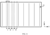
- FIG. 6 is a plan view of a solar cell according to some embodiments of the present disclosure. As shown in FIG. 1 and FIG. 6 , the body has multiple first regions I and multiple second regions II, and the first regions I are arranged alternately with the second regions II along a width direction Y of the solar cell.
- the first region I and the second region II are spaced apart along the width direction Y of the solar cell, so that the first region I corresponds to the first electrode 21, thereby effectively reducing an increase in the carrier recombination caused by damages of the first doped conductive layer 13 caused by the first electrode 21 and ensuring the efficiency of the solar cell.
- a width D1 of the first region I satisfies: 10 ⁇ m ⁇ D1 ⁇ 200 ⁇ m.
- the width D1 may be 10 ⁇ m, 20 ⁇ m, 50 ⁇ m, 100 ⁇ m, 150 ⁇ m, 200 ⁇ m, or the like.
- FIG. 6 also shows the length direction Z of the solar cell, and the second electrode 22 extends along the length direction Z.
- the width D1 of the first region I should not be excessively large or excessively small. If the width D1 is excessively large (e.g., greater than 200 ⁇ m), the width of the second region II is excessively small, which affects the transverse transport capability of the solar cell. If the width D1 is excessively small (e.g., less than 10 ⁇ m), the first region I cannot completely cover the first electrode 21 along a thickness direction X of the solar cell, so that the recombination of the carriers cannot be effectively reduced, which affects the efficiency of the solar cell.
- a ratio of a width D2 of the first electrode 21 to a width D1 of the first region I satisfies: 0.3 ⁇ D2/D1 ⁇ 1.
- the ratio of the width D2 to the width D1 may be 0.3, 0.5, 0.7, 0.9, 1, or the like.
- the ratio of the width D2 of the first electrode 21 to the width D1 of the first region I should not be excessively large or excessively small. If the ratio of the width D2 to the width D1 is excessively large (e.g., greater than 1), the first region I cannot completely cover the first electrode 21 along the thickness direction X of the solar cell, so that the recombination of the carriers cannot be effectively reduced, which affects the efficiency of the solar cell. If the ratio of the width D2 to the width D1 is excessively small (e.g., less than 0.3), the width D1 of the first region I is excessively large, and the width of the second region II is excessively small, which affects the transverse transport capability of the solar cell.
- the ratio of a width D2 of the first electrode 21 to the width D1 of the first region I satisfies: 0.3 ⁇ D2/D1 ⁇ 1, the transport capability of the solar cell can be ensured.
- the body further includes an emitter 16 arranged on a surface of the substrate 11 away from the first tunneling layer 12, and the solar cell further includes a second electrode 22 electrically connected to the emitter 16.
- the substrate 11 and the emitter 16 can jointly form a PN junction structure.
- the substrate 11 may be a P-type silicon substrate
- the emitter 16 may be an N-type emitter
- the P-type silicon substrate and the N-type emitter may jointly form a built-in electric field of the PN junction.
- the substrate 11 may be an N-type silicon substrate
- the emitter 16 may be a P-type emitter.
- the body further includes a first passivation layer 15 and a second passivation layer 17, the first passivation layer 15 is arranged on a side of the first doped conductive layer 13 away from the substrate 11, and the second passivation layer 17 is arranged on a side of the emitter 16 away from the substrate 11.
- the first passivation layer 15 can passivate a surface of the first doped conductive layer 13 away from the substrate 11, and the second passivation layer 17 can passivate a surface of the emitter 16 away from the substrate 11, thereby reducing a recombination rate of the carriers of the first doped conductive layer 13 and a recombination rate of the carriers of the emitter 16 respectively, and improving the photoelectric conversion efficiency of the solar cell.
- each of the first passivation layer 15 and the second passivation layer 17 may be a single layer such as a silicon oxide layer, a silicon nitride layer, an aluminum oxide layer, and a silicon oxynitride layer.
- each of the first passivation layer 15 and the second passivation layer 17 may be a stacked structure including at least one or more of a silicon oxide layer, a silicon nitride layer, an aluminum oxide layer, and a silicon oxynitride layer.
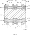
- the body further includes: a second tunneling layer 12', a third doped conductive layer 13', and a fourth doped conductive layer 14'.
- the second tunneling layer 12' is arranged on a side of the substrate 11 away from the first tunneling layer 12, and a thickness of the second tunneling layer 12' in the first region I is greater than that in the second region II.
- the third doped conductive layer 13' is arranged on a surface of the second tunneling layer 12' away from the substrate 11.
- the fourth doped conductive layer 14' is located on a side of the substrate 11 adjacent to the second tunneling layer 12', and a thickness of the fourth doped conductive layer 14' in the first region I is less than that in the second region II.
- the solar cell further includes a third electrode 21', and the third electrode 21' is electrically connected to the third doped conductive layer 13'.
- the second tunneling layer 12' is a tunneling layer for majority carriers, and at the same time chemically passivates the substrate 11 to reduce interface states.
- the third doped conductive layer 13' can form energy band bending, realize selective transport of the carriers, and reduce recombination losses of the carriers.
- the third electrode 21' is electrically connected to the third doped conductive layer 13', and is not in contact with the second tunneling layer 12', thereby maintaining good interface passivation. A small part of the dopant element in the third doped conductive layer 13' may enter the substrate 11 through the second tunneling layer 12', and form the fourth doped conductive layer 14' on a surface of the substrate 11.
- the thickness of the second tunneling layer 12' in the first region I is different from that in the second region II, so that the thickness of the fourth doped conductive layer 14' formed on the surface of the substrate 11 and formed by the dopant element from the third doped conductive layer 13' is different.
- the thickness of the second tunneling layer 12' in the first region I is greater than that in the second region II, so that the thickness of the fourth doped conductive layer 14' in the first region I is less than that in the second region II.
- the third electrode 21' extends into the third doped conductive layer 13', which damages a structure of the third doped conductive layer 13' and increases carrier recombination.
- a thicker second tunneling layer 12' is arranged on a side of the third electrode 21' adjacent to the substrate 11, which can improve a passivation effect of the region, reduce the thickness of the fourth doped conductive layer 14', reduce the carrier recombination, and improve the photoelectric conversion efficiency of the solar cell.
- the thinner second tunneling layer 12' improves transport capability of the carriers from the substrate 11 to the third doped conductive layer 13', and makes the fourth doped conductive layer 14' thicker, which reduces sheet resistance of the fourth doped conductive layer 14', improves the transverse transport capability of the carriers, and improves the photoelectric conversion efficiency of the solar cell.
- the second tunneling layer 12' is a silicon oxide layer (SiO x ), with a thickness ranging from 0.5 nm to 2.5 nm.
- the thickness of the second tunneling layer 12' may be 0.5 nm, 1 nm, 1.5 nm, 2 nm, 2.5 nm, or the like.
- the third doped conductive layer 13' may be amorphous silicon, microcrystalline silicon, polycrystalline silicon, or the like containing a dopant element.
- the dopant element may be an N-type dopant element such as a Group V element including P, As, Bi, and Sb, or a P-type dopant element such as a Group III element including B, Al, Ga, and In.
- the third doped conductive layer 13' and the substrate 11 should be doped with different types of dopant elements, so that the third doped conductive layer 13' and the substrate 11 together form a built-in electric field structure that functions as a PN junction.
- the body further includes a first passivation layer 15 and a third passivation layer 15', the first passivation layer 15 is arranged on a side of the first doped conductive layer 13 away from the substrate 11, and the third passivation layer 15' is arranged on a side of the third doped conductive layer 13' away from the substrate 11.
- the first passivation layer 15 can passivate a surface of the first doped conductive layer 13 away from the substrate 11, thereby reducing a recombination rate of the carriers of the first doped conductive layer 13, and improving the photoelectric conversion efficiency of the solar cell.
- the third passivation layer 15' can passivate a surface of the third doped conductive layer 13' away from the substrate 11, thereby reducing a recombination rate of the carriers of the third doped conductive layer 13', and improving the photoelectric conversion efficiency of the solar cell.
- each of the first passivation layer 15 and the third passivation layer 15' may be a single layer such as a silicon oxide layer, a silicon nitride layer, an aluminum oxide layer, and a silicon oxynitride layer.
- each of the first passivation layer 15 and the third passivation layer 15' may be a stacked structure including at least one or more of a silicon oxide layer, a silicon nitride layer, an aluminum oxide layer, and a silicon oxynitride layer.
- the second tunneling layer 12' in the first region I protrudes towards the third doped conductive layer 13' with respect to the second tunneling layer 12' in the second region II; and the fourth doped conductive layer 14' in the second region II protrudes towards the substrate 11 with respect to the fourth doped conductive layer 14' in the first region I.
- the second tunneling layer 12' in the first region I protrudes towards the substrate 11 with respect to the second tunneling layer 12' in the second region II; and the fourth doped conductive layer 14' in the second region II protrudes towards the third doped conductive layer 13' with respect to the fourth doped conductive layer 14' in the first region I.
- the second tunneling layer 12' in the first region I protrudes towards the third doped conductive layer 13' with respect to the second tunneling layer 12' in the second region II, so that the fourth doped conductive layer 14' in the second region II protrudes towards the substrate 11 with respect to the fourth doped conductive layer 14' in the first region I. That is, an interface between the second tunneling layer 12' and the fourth doped conductive layer 14' is a substantially flat plane.
- the second tunneling layer 12' in the first region I protrudes towards the substrate 11 with respect to the second tunneling layer 12' in the second region II, so that the fourth doped conductive layer 14' in the second region II protrudes towards the third doped conductive layer 13' with respect to the fourth doped conductive layer 14' in the first region I. That is, an interface between the second tunneling layer 12' and the third doped conductive layer 13' is a substantially flat plane, and a surface of the fourth doped conductive layer 14' away from the second tunneling layer 12' is a substantially flat plane.
- the photovoltaic module includes: a solar cell string 110, an encapsulation layer 120, and a cover plate 130.
- the solar cell string 110 includes a plurality of solar cells connected to one another.
- the encapsulation layer 120 is configured to cover a surface of the solar cell string 110.
- the encapsulation layer 120 covers at least the top and bottom surfaces of the solar cell string 110.
- the cover plate 130 is configured to cover a surface of the encapsulation layer 120 away from the solar cell string 110.
- the plurality of solar cells in the solar cell string 110 are electrically connected in series and/or in parallel.
- the cover plate 130, the encapsulation layer 120, and the solar cell string 110 may be laminated in a certain order through a lamination process to obtain a laminated assembly, and then a frame may be mounted on the laminated assembly to form the photovoltaic module, which is easy to transport and use.
Landscapes
- Photovoltaic Devices (AREA)
- Life Sciences & Earth Sciences (AREA)
- Engineering & Computer Science (AREA)
- Sustainable Development (AREA)
- Sustainable Energy (AREA)
Applications Claiming Priority (1)
| Application Number | Priority Date | Filing Date | Title |
|---|---|---|---|
| CN202211603377.7A CN115692534B (zh) | 2022-12-14 | 2022-12-14 | 一种太阳能电池及光伏组件 |
Publications (2)
| Publication Number | Publication Date |
|---|---|
| EP4386864A1 true EP4386864A1 (de) | 2024-06-19 |
| EP4386864B1 EP4386864B1 (de) | 2025-06-04 |
Family
ID=85055418
Family Applications (1)
| Application Number | Title | Priority Date | Filing Date |
|---|---|---|---|
| EP23196106.1A Active EP4386864B1 (de) | 2022-12-14 | 2023-09-07 | Solarzelle und fotovoltaisches modul |
Country Status (3)
| Country | Link |
|---|---|
| US (1) | US20240204121A1 (de) |
| EP (1) | EP4386864B1 (de) |
| CN (1) | CN115692534B (de) |
Cited By (1)
| Publication number | Priority date | Publication date | Assignee | Title |
|---|---|---|---|---|
| CN120583739A (zh) * | 2025-07-31 | 2025-09-02 | 安徽晶科能源有限公司 | 太阳能电池及其制造方法、叠层电池和光伏组件 |
Families Citing this family (4)
| Publication number | Priority date | Publication date | Assignee | Title |
|---|---|---|---|---|
| CN117317041A (zh) * | 2023-11-29 | 2023-12-29 | 浙江晶科能源有限公司 | 太阳能电池及光伏组件 |
| CN118263339B (zh) * | 2024-05-28 | 2024-08-30 | 天合光能股份有限公司 | 一种太阳能电池和太阳能电池的制造方法 |
| CN118867057B (zh) * | 2024-09-24 | 2024-12-20 | 玉环晶科能源有限公司 | 太阳能电池及其制备方法 |
| CN121772354A (zh) * | 2025-01-03 | 2026-03-31 | 浙江晶科能源有限公司 | 光伏组件 |
Citations (4)
| Publication number | Priority date | Publication date | Assignee | Title |
|---|---|---|---|---|
| US20160005900A1 (en) * | 2014-07-07 | 2016-01-07 | Lg Electronics Inc. | Solar cell |
| KR20160111624A (ko) * | 2015-03-17 | 2016-09-27 | 엘지전자 주식회사 | 태양 전지 및 이의 제조 방법 |
| US20220140160A1 (en) * | 2020-10-30 | 2022-05-05 | Zhejiang Jinko Solar Co., Ltd. | Solar cell |
| CN114823951A (zh) * | 2022-06-28 | 2022-07-29 | 晶科能源(海宁)有限公司 | 太阳能电池及光伏组件 |
Family Cites Families (11)
| Publication number | Priority date | Publication date | Assignee | Title |
|---|---|---|---|---|
| JP5566502B2 (ja) * | 2013-05-10 | 2014-08-06 | 京セラ株式会社 | 太陽電池素子 |
| US20150236174A1 (en) * | 2013-12-02 | 2015-08-20 | Solexel, Inc. | Single passivated contacts for back contact back junction solar cells |
| US9337369B2 (en) * | 2014-03-28 | 2016-05-10 | Sunpower Corporation | Solar cells with tunnel dielectrics |
| JP6369680B2 (ja) * | 2014-05-30 | 2018-08-08 | パナソニックIpマネジメント株式会社 | 太陽電池 |
| CN106575676B (zh) * | 2014-07-17 | 2019-06-28 | 光城公司 | 具有叉指背接触的太阳能电池 |
| TWI662715B (zh) * | 2017-10-27 | 2019-06-11 | 財團法人工業技術研究院 | 太陽能電池 |
| CN109713065B (zh) * | 2018-12-28 | 2023-10-31 | 泰州中来光电科技有限公司 | 一种印刷金属电极的钝化太阳能电池及其制备方法 |
| CN210897294U (zh) * | 2019-10-29 | 2020-06-30 | 苏州阿特斯阳光电力科技有限公司 | 太阳能电池 |
| CN111524983B (zh) * | 2020-04-03 | 2021-07-27 | 常州大学 | 一种双面选择性发射极高效晶硅电池及其制备方法 |
| CN113571604B (zh) * | 2021-09-27 | 2022-01-25 | 浙江晶科能源有限公司 | 光伏电池及其制备方法、光伏组件 |
| CN115458617B (zh) * | 2022-11-04 | 2023-03-24 | 浙江晶科能源有限公司 | 太阳能电池及光伏组件 |
-
2022
- 2022-12-14 CN CN202211603377.7A patent/CN115692534B/zh active Active
-
2023
- 2023-08-28 US US18/457,333 patent/US20240204121A1/en active Pending
- 2023-09-07 EP EP23196106.1A patent/EP4386864B1/de active Active
Patent Citations (4)
| Publication number | Priority date | Publication date | Assignee | Title |
|---|---|---|---|---|
| US20160005900A1 (en) * | 2014-07-07 | 2016-01-07 | Lg Electronics Inc. | Solar cell |
| KR20160111624A (ko) * | 2015-03-17 | 2016-09-27 | 엘지전자 주식회사 | 태양 전지 및 이의 제조 방법 |
| US20220140160A1 (en) * | 2020-10-30 | 2022-05-05 | Zhejiang Jinko Solar Co., Ltd. | Solar cell |
| CN114823951A (zh) * | 2022-06-28 | 2022-07-29 | 晶科能源(海宁)有限公司 | 太阳能电池及光伏组件 |
Cited By (1)
| Publication number | Priority date | Publication date | Assignee | Title |
|---|---|---|---|---|
| CN120583739A (zh) * | 2025-07-31 | 2025-09-02 | 安徽晶科能源有限公司 | 太阳能电池及其制造方法、叠层电池和光伏组件 |
Also Published As
| Publication number | Publication date |
|---|---|
| US20240204121A1 (en) | 2024-06-20 |
| EP4386864B1 (de) | 2025-06-04 |
| CN115692534B (zh) | 2023-03-28 |
| CN115692534A (zh) | 2023-02-03 |
Similar Documents
| Publication | Publication Date | Title |
|---|---|---|
| EP4386864A1 (de) | Solarzelle und fotovoltaisches modul | |
| US12027641B2 (en) | Solar cell and photovoltaic module | |
| CN115985980B (zh) | 一种太阳能电池及光伏组件 | |
| US20190245101A1 (en) | Solar cell | |
| US12176448B2 (en) | Photovoltaic cell and photovoltaic module | |
| US20240395949A1 (en) | Solar cell, photovoltaic module, and method for preparing photovoltaic module | |
| EP2816609B1 (de) | Solarzelle | |
| EP4300599B1 (de) | Solarzelle und fotovoltaisches modul | |
| EP4579761B1 (de) | Solarzelle, verfahren zur herstellung einer solarzelle und fotovoltaisches modul | |
| CN118073439A (zh) | 太阳能电池及光伏组件 | |
| CN115347059A (zh) | 一种太阳能电池及光伏组件 | |
| CN120379391B (zh) | 一种背接触电池、背接触叠层电池及光伏组件 | |
| EP4579762A1 (de) | Solarzelle und fotovoltaisches modul | |
| CN121152333B (zh) | 光伏组件 | |
| EP4622424A1 (de) | Solarzelle und fotovoltaisches modul | |
| CN120358841A (zh) | 一种背接触电池、背接触叠层电池和光伏组件 | |
| CN121712123A (zh) | 一种光伏组件 | |
| CN118073440A (zh) | 光伏组件 |
Legal Events
| Date | Code | Title | Description |
|---|---|---|---|
| PUAI | Public reference made under article 153(3) epc to a published international application that has entered the european phase |
Free format text: ORIGINAL CODE: 0009012 |
|
| STAA | Information on the status of an ep patent application or granted ep patent |
Free format text: STATUS: REQUEST FOR EXAMINATION WAS MADE |
|
| 17P | Request for examination filed |
Effective date: 20240328 |
|
| AK | Designated contracting states |
Kind code of ref document: A1 Designated state(s): AL AT BE BG CH CY CZ DE DK EE ES FI FR GB GR HR HU IE IS IT LI LT LU LV MC ME MK MT NL NO PL PT RO RS SE SI SK SM TR |
|
| REG | Reference to a national code |
Ref country code: DE Ref legal event code: R079 Free format text: PREVIOUS MAIN CLASS: H01L0031021600 Ipc: H10F0077300000 Ref document number: 602023003817 Country of ref document: DE |
|
| GRAP | Despatch of communication of intention to grant a patent |
Free format text: ORIGINAL CODE: EPIDOSNIGR1 |
|
| STAA | Information on the status of an ep patent application or granted ep patent |
Free format text: STATUS: GRANT OF PATENT IS INTENDED |
|
| INTG | Intention to grant announced |
Effective date: 20250203 |
|
| RIC1 | Information provided on ipc code assigned before grant |
Ipc: H10F 71/00 20250101ALI20250124BHEP Ipc: H10F 10/166 20250101ALI20250124BHEP Ipc: H10F 10/14 20250101ALI20250124BHEP Ipc: H10F 77/30 20250101AFI20250124BHEP |
|
| GRAS | Grant fee paid |
Free format text: ORIGINAL CODE: EPIDOSNIGR3 |
|
| GRAA | (expected) grant |
Free format text: ORIGINAL CODE: 0009210 |
|
| STAA | Information on the status of an ep patent application or granted ep patent |
Free format text: STATUS: THE PATENT HAS BEEN GRANTED |
|
| AK | Designated contracting states |
Kind code of ref document: B1 Designated state(s): AL AT BE BG CH CY CZ DE DK EE ES FI FR GB GR HR HU IE IS IT LI LT LU LV MC ME MK MT NL NO PL PT RO RS SE SI SK SM TR |
|
| REG | Reference to a national code |
Ref country code: GB Ref legal event code: FG4D |
|
| REG | Reference to a national code |
Ref country code: CH Ref legal event code: EP |
|
| REG | Reference to a national code |
Ref country code: DE Ref legal event code: R096 Ref document number: 602023003817 Country of ref document: DE |
|
| REG | Reference to a national code |
Ref country code: IE Ref legal event code: FG4D |
|
| REG | Reference to a national code |
Ref country code: NL Ref legal event code: MP Effective date: 20250604 |
|
| PG25 | Lapsed in a contracting state [announced via postgrant information from national office to epo] |
Ref country code: ES Free format text: LAPSE BECAUSE OF FAILURE TO SUBMIT A TRANSLATION OF THE DESCRIPTION OR TO PAY THE FEE WITHIN THE PRESCRIBED TIME-LIMIT Effective date: 20250604 Ref country code: FI Free format text: LAPSE BECAUSE OF FAILURE TO SUBMIT A TRANSLATION OF THE DESCRIPTION OR TO PAY THE FEE WITHIN THE PRESCRIBED TIME-LIMIT Effective date: 20250604 |
|
| PGFP | Annual fee paid to national office [announced via postgrant information from national office to epo] |
Ref country code: DE Payment date: 20250919 Year of fee payment: 3 |
|
| REG | Reference to a national code |
Ref country code: LT Ref legal event code: MG9D |
|
| PG25 | Lapsed in a contracting state [announced via postgrant information from national office to epo] |
Ref country code: GR Free format text: LAPSE BECAUSE OF FAILURE TO SUBMIT A TRANSLATION OF THE DESCRIPTION OR TO PAY THE FEE WITHIN THE PRESCRIBED TIME-LIMIT Effective date: 20250905 Ref country code: NO Free format text: LAPSE BECAUSE OF FAILURE TO SUBMIT A TRANSLATION OF THE DESCRIPTION OR TO PAY THE FEE WITHIN THE PRESCRIBED TIME-LIMIT Effective date: 20250904 |
|
| PG25 | Lapsed in a contracting state [announced via postgrant information from national office to epo] |
Ref country code: PL Free format text: LAPSE BECAUSE OF FAILURE TO SUBMIT A TRANSLATION OF THE DESCRIPTION OR TO PAY THE FEE WITHIN THE PRESCRIBED TIME-LIMIT Effective date: 20250604 |
|
| PG25 | Lapsed in a contracting state [announced via postgrant information from national office to epo] |
Ref country code: BG Free format text: LAPSE BECAUSE OF FAILURE TO SUBMIT A TRANSLATION OF THE DESCRIPTION OR TO PAY THE FEE WITHIN THE PRESCRIBED TIME-LIMIT Effective date: 20250604 |
|
| PG25 | Lapsed in a contracting state [announced via postgrant information from national office to epo] |
Ref country code: HR Free format text: LAPSE BECAUSE OF FAILURE TO SUBMIT A TRANSLATION OF THE DESCRIPTION OR TO PAY THE FEE WITHIN THE PRESCRIBED TIME-LIMIT Effective date: 20250604 |
|
| PGFP | Annual fee paid to national office [announced via postgrant information from national office to epo] |
Ref country code: AT Payment date: 20251020 Year of fee payment: 3 |
|
| PG25 | Lapsed in a contracting state [announced via postgrant information from national office to epo] |
Ref country code: RS Free format text: LAPSE BECAUSE OF FAILURE TO SUBMIT A TRANSLATION OF THE DESCRIPTION OR TO PAY THE FEE WITHIN THE PRESCRIBED TIME-LIMIT Effective date: 20250904 |
|
| PG25 | Lapsed in a contracting state [announced via postgrant information from national office to epo] |
Ref country code: LV Free format text: LAPSE BECAUSE OF FAILURE TO SUBMIT A TRANSLATION OF THE DESCRIPTION OR TO PAY THE FEE WITHIN THE PRESCRIBED TIME-LIMIT Effective date: 20250604 |
|
| PG25 | Lapsed in a contracting state [announced via postgrant information from national office to epo] |
Ref country code: NL Free format text: LAPSE BECAUSE OF FAILURE TO SUBMIT A TRANSLATION OF THE DESCRIPTION OR TO PAY THE FEE WITHIN THE PRESCRIBED TIME-LIMIT Effective date: 20250604 |
|
| PG25 | Lapsed in a contracting state [announced via postgrant information from national office to epo] |
Ref country code: PT Free format text: LAPSE BECAUSE OF FAILURE TO SUBMIT A TRANSLATION OF THE DESCRIPTION OR TO PAY THE FEE WITHIN THE PRESCRIBED TIME-LIMIT Effective date: 20251006 |
|
| REG | Reference to a national code |
Ref country code: AT Ref legal event code: MK05 Ref document number: 1801630 Country of ref document: AT Kind code of ref document: T Effective date: 20250604 |
|
| PG25 | Lapsed in a contracting state [announced via postgrant information from national office to epo] |
Ref country code: IS Free format text: LAPSE BECAUSE OF FAILURE TO SUBMIT A TRANSLATION OF THE DESCRIPTION OR TO PAY THE FEE WITHIN THE PRESCRIBED TIME-LIMIT Effective date: 20251004 |
|
| PG25 | Lapsed in a contracting state [announced via postgrant information from national office to epo] |
Ref country code: AT Free format text: LAPSE BECAUSE OF FAILURE TO SUBMIT A TRANSLATION OF THE DESCRIPTION OR TO PAY THE FEE WITHIN THE PRESCRIBED TIME-LIMIT Effective date: 20250604 Ref country code: SM Free format text: LAPSE BECAUSE OF FAILURE TO SUBMIT A TRANSLATION OF THE DESCRIPTION OR TO PAY THE FEE WITHIN THE PRESCRIBED TIME-LIMIT Effective date: 20250604 |
|
| PG25 | Lapsed in a contracting state [announced via postgrant information from national office to epo] |
Ref country code: CZ Free format text: LAPSE BECAUSE OF FAILURE TO SUBMIT A TRANSLATION OF THE DESCRIPTION OR TO PAY THE FEE WITHIN THE PRESCRIBED TIME-LIMIT Effective date: 20250604 |
|
| PG25 | Lapsed in a contracting state [announced via postgrant information from national office to epo] |
Ref country code: EE Free format text: LAPSE BECAUSE OF FAILURE TO SUBMIT A TRANSLATION OF THE DESCRIPTION OR TO PAY THE FEE WITHIN THE PRESCRIBED TIME-LIMIT Effective date: 20250604 |
|
| PG25 | Lapsed in a contracting state [announced via postgrant information from national office to epo] |
Ref country code: SK Free format text: LAPSE BECAUSE OF FAILURE TO SUBMIT A TRANSLATION OF THE DESCRIPTION OR TO PAY THE FEE WITHIN THE PRESCRIBED TIME-LIMIT Effective date: 20250604 |
|
| PG25 | Lapsed in a contracting state [announced via postgrant information from national office to epo] |
Ref country code: IT Free format text: LAPSE BECAUSE OF FAILURE TO SUBMIT A TRANSLATION OF THE DESCRIPTION OR TO PAY THE FEE WITHIN THE PRESCRIBED TIME-LIMIT Effective date: 20250604 |
|
| REG | Reference to a national code |
Ref country code: DE Ref legal event code: R097 Ref document number: 602023003817 Country of ref document: DE |
|
| PG25 | Lapsed in a contracting state [announced via postgrant information from national office to epo] |
Ref country code: RO Free format text: LAPSE BECAUSE OF FAILURE TO SUBMIT A TRANSLATION OF THE DESCRIPTION OR TO PAY THE FEE WITHIN THE PRESCRIBED TIME-LIMIT Effective date: 20250604 |
|
| PLBE | No opposition filed within time limit |
Free format text: ORIGINAL CODE: 0009261 |
|
| STAA | Information on the status of an ep patent application or granted ep patent |
Free format text: STATUS: NO OPPOSITION FILED WITHIN TIME LIMIT |
|
| PG25 | Lapsed in a contracting state [announced via postgrant information from national office to epo] |
Ref country code: DK Free format text: LAPSE BECAUSE OF FAILURE TO SUBMIT A TRANSLATION OF THE DESCRIPTION OR TO PAY THE FEE WITHIN THE PRESCRIBED TIME-LIMIT Effective date: 20250604 |
|
| REG | Reference to a national code |
Ref country code: CH Ref legal event code: L10 Free format text: ST27 STATUS EVENT CODE: U-0-0-L10-L00 (AS PROVIDED BY THE NATIONAL OFFICE) Effective date: 20260416 |