EP4390480A1 - Mehrstufige rückausbreitungsvorrichtung - Google Patents
Mehrstufige rückausbreitungsvorrichtung Download PDFInfo
- Publication number
- EP4390480A1 EP4390480A1 EP23216207.3A EP23216207A EP4390480A1 EP 4390480 A1 EP4390480 A1 EP 4390480A1 EP 23216207 A EP23216207 A EP 23216207A EP 4390480 A1 EP4390480 A1 EP 4390480A1
- Authority
- EP
- European Patent Office
- Prior art keywords
- level
- waveguides
- light radiation
- guide
- addressing
- Prior art date
- Legal status (The legal status is an assumption and is not a legal conclusion. Google has not performed a legal analysis and makes no representation as to the accuracy of the status listed.)
- Pending
Links
Images



Classifications
-
- G—PHYSICS
- G02—OPTICS
- G02B—OPTICAL ELEMENTS, SYSTEMS OR APPARATUS
- G02B6/00—Light guides; Structural details of arrangements comprising light guides and other optical elements, e.g. couplings
- G02B6/10—Light guides; Structural details of arrangements comprising light guides and other optical elements, e.g. couplings of the optical waveguide type
- G02B6/12—Light guides; Structural details of arrangements comprising light guides and other optical elements, e.g. couplings of the optical waveguide type of the integrated circuit kind
- G02B6/12002—Three-dimensional structures
-
- G—PHYSICS
- G02—OPTICS
- G02B—OPTICAL ELEMENTS, SYSTEMS OR APPARATUS
- G02B6/00—Light guides; Structural details of arrangements comprising light guides and other optical elements, e.g. couplings
- G02B6/24—Coupling light guides
- G02B6/26—Optical coupling means
-
- G—PHYSICS
- G02—OPTICS
- G02B—OPTICAL ELEMENTS, SYSTEMS OR APPARATUS
- G02B27/00—Optical systems or apparatus not provided for by any of the groups G02B1/00 - G02B26/00, G02B30/00
- G02B27/01—Head-up displays
- G02B27/017—Head mounted
- G02B27/0172—Head mounted characterised by optical features
-
- G—PHYSICS
- G02—OPTICS
- G02B—OPTICAL ELEMENTS, SYSTEMS OR APPARATUS
- G02B6/00—Light guides; Structural details of arrangements comprising light guides and other optical elements, e.g. couplings
- G02B6/10—Light guides; Structural details of arrangements comprising light guides and other optical elements, e.g. couplings of the optical waveguide type
- G02B6/12—Light guides; Structural details of arrangements comprising light guides and other optical elements, e.g. couplings of the optical waveguide type of the integrated circuit kind
-
- G—PHYSICS
- G02—OPTICS
- G02B—OPTICAL ELEMENTS, SYSTEMS OR APPARATUS
- G02B6/00—Light guides; Structural details of arrangements comprising light guides and other optical elements, e.g. couplings
- G02B6/10—Light guides; Structural details of arrangements comprising light guides and other optical elements, e.g. couplings of the optical waveguide type
- G02B6/12—Light guides; Structural details of arrangements comprising light guides and other optical elements, e.g. couplings of the optical waveguide type of the integrated circuit kind
- G02B6/122—Basic optical elements, e.g. light-guiding paths
- G02B6/125—Bends, branchings or intersections
-
- G—PHYSICS
- G02—OPTICS
- G02F—OPTICAL DEVICES OR ARRANGEMENTS FOR THE CONTROL OF LIGHT BY MODIFICATION OF THE OPTICAL PROPERTIES OF THE MEDIA OF THE ELEMENTS INVOLVED THEREIN; NON-LINEAR OPTICS; FREQUENCY-CHANGING OF LIGHT; OPTICAL LOGIC ELEMENTS; OPTICAL ANALOGUE/DIGITAL CONVERTERS
- G02F1/00—Devices or arrangements for the control of the intensity, colour, phase, polarisation or direction of light arriving from an independent light source, e.g. switching, gating or modulating; Non-linear optics
- G02F1/01—Devices or arrangements for the control of the intensity, colour, phase, polarisation or direction of light arriving from an independent light source, e.g. switching, gating or modulating; Non-linear optics for the control of the intensity, phase, polarisation or colour
- G02F1/13—Devices or arrangements for the control of the intensity, colour, phase, polarisation or direction of light arriving from an independent light source, e.g. switching, gating or modulating; Non-linear optics for the control of the intensity, phase, polarisation or colour based on liquid crystals, e.g. single liquid crystal display cells
-
- G—PHYSICS
- G03—PHOTOGRAPHY; CINEMATOGRAPHY; ANALOGOUS TECHNIQUES USING WAVES OTHER THAN OPTICAL WAVES; ELECTROGRAPHY; HOLOGRAPHY
- G03B—APPARATUS OR ARRANGEMENTS FOR TAKING PHOTOGRAPHS OR FOR PROJECTING OR VIEWING THEM; APPARATUS OR ARRANGEMENTS EMPLOYING ANALOGOUS TECHNIQUES USING WAVES OTHER THAN OPTICAL WAVES; ACCESSORIES THEREFOR
- G03B21/00—Projectors or projection-type viewers; Accessories therefor
- G03B21/005—Projectors using an electronic spatial light modulator but not peculiar thereto
- G03B21/006—Projectors using an electronic spatial light modulator but not peculiar thereto using LCD's
-
- G—PHYSICS
- G02—OPTICS
- G02B—OPTICAL ELEMENTS, SYSTEMS OR APPARATUS
- G02B6/00—Light guides; Structural details of arrangements comprising light guides and other optical elements, e.g. couplings
- G02B6/10—Light guides; Structural details of arrangements comprising light guides and other optical elements, e.g. couplings of the optical waveguide type
- G02B6/12—Light guides; Structural details of arrangements comprising light guides and other optical elements, e.g. couplings of the optical waveguide type of the integrated circuit kind
- G02B2006/12083—Constructional arrangements
- G02B2006/12104—Mirror; Reflectors or the like
-
- G—PHYSICS
- G02—OPTICS
- G02B—OPTICAL ELEMENTS, SYSTEMS OR APPARATUS
- G02B6/00—Light guides; Structural details of arrangements comprising light guides and other optical elements, e.g. couplings
- G02B6/0001—Light guides; Structural details of arrangements comprising light guides and other optical elements, e.g. couplings specially adapted for lighting devices or systems
- G02B6/0011—Light guides; Structural details of arrangements comprising light guides and other optical elements, e.g. couplings specially adapted for lighting devices or systems the light guides being planar or of plate-like form
- G02B6/0075—Arrangements of multiple light guides
- G02B6/0076—Stacked arrangements of multiple light guides of the same or different cross-sectional area
Definitions
- the field of the invention is that of integrated photonics.
- the invention finds a particular application in a compact addressing device for a projector, in particular for a retinal projector.
- FIG 1 illustrates a classic photonic projector architecture, comprising an addressing part a1 attached to a projection part p1.
- the addressing part a1 typically comprises a plurality of waveguides 11 coming from a main waveguide, for example by means of a balanced tree of multimode interferometers MMI (Multimode Interferometer).
- the projection part p1 typically comprises a dense distribution of waveguides (4096 guides on the figure 1 which are not visible individually) made of silicon nitride (Si3N4) with a rectangular section, spaced regularly.
- Such a photonic architecture occupies a significant surface area of the chip or substrate.
- the addressing part a1 has a non-negligible surface area compared to that of the projection part p1.
- An objective of the invention is to meet this need.
- an object of the invention is a multilevel back-propagation device making it possible to superimpose different levels of waveguides, for example an addressing level and a projection level.
- Another object of the invention is an integrated projector comprising a superimposed addressing level and a projection level.
- the classic projector photonic architecture illustrated in figure 1 can thus be “folded” as illustrated in figure 2 .
- the projection level p2 located on the second level is here superimposed on the addressing level a1 located on the first level.
- the light radiation propagates from left to right in the addressing level a1; it is coupled to the projection level p2 in the coupling region 3, and reflected by the reflector 4; the light radiation propagates from right to left in the projection level p2.
- the multilevel feedback device has significantly improved compactness. This advantageously makes it possible to reduce the bulk of a photonic architecture comprising such a multilevel back-coupling device.
- an optical projection system comprising a multilevel feedback device as described above, in which the second level corresponds to a projection level.
- a system further comprises an electrode below the projection level.
- This electrode called the lower electrode, is typically used to activate extraction elements on the surface of the device. Activation can in particular be done by associating a counter-electrode attached with a component placed above the optical projection system. Activation is done by example with a layer of liquid crystal located between the lower electrode and the counter electrode This makes it possible to extract part of the light radiation guided in the waveguides of the projection level, in particular when applying a electrical voltage between the lower electrode and the counter electrode, in order to emit light points and display an image.
- the reflector is formed by an interruption of the first and second waveguides in a plane normal to the first and second directions of propagation.
- the reflector is formed by a block interrupting the first and second waveguides, said block being based on a reflective material such as aluminum.
- a reflector is not wavelength selective. It is advantageously broadband. Such a reflector can therefore be used for a large number of applications, for example in the visible and in the infrared.
- the coupling portion has a length Lc/2 along a direction of propagation of the electromagnetic radiation, Le being the characteristic coupling length for a transfer of a mode of propagation of the electromagnetic radiation from the first waveguide to the second waveguide.
- Le being the characteristic coupling length for a transfer of a mode of propagation of the electromagnetic radiation from the first waveguide to the second waveguide.
- the reflector is formed by a first Bragg mirror attached to the first waveguide and by a second Bragg mirror attached to the second waveguide, said first and second Bragg mirrors being superposed in the normal direction.
- a reflector can be easily manufactured by microelectronics processes and technologies. It is also wavelength selective. This makes it possible, for example, to filter light radiation and/or to create sub-levels dedicated to light radiation of different wavelengths.
- the coupling portion has a length Lc/2 - ⁇ along a direction of propagation of the electromagnetic radiation, Le being the characteristic coupling length for a transfer of a mode of propagation of the electromagnetic radiation of the first waveguide to the second waveguide, and ⁇ > 0 being a penetration length of the mode in the first and second Bragg mirrors.
- the length of the coupling portion is reduced here, due to the penetration of the propagation mode into the Bragg mirror(s).
- the first level corresponds to an addressing level and the lower electrode is located below the addressing level. This makes it possible to limit or eliminate absorption phenomena linked to the lower electrode.
- the first level corresponds to an addressing level and the lower electrode is located between the projection level and the addressing level. This allows to bring the lower electrode closer to the projection level. This makes it possible to reduce the voltage to be applied to extract the light radiation.
- the first level corresponds to an intermediate level and the lower electrode is located at the same level as the intermediate level, and the system further comprises an addressing level located below the lower electrode and the level intermediate.
- an addressing level located below the lower electrode and the level intermediate. This makes it possible to reduce optical losses while reducing the voltage to be applied to extract the light radiation.
- the use of an intermediate level between the addressing level and the projection level also makes it possible to optimize the coupling and reduce the length of the coupling portion.
- the at least one first level comprises a first addressing level comprising waveguides configured to guide a propagation of a first light radiation having a first wavelength ⁇ 1, a second addressing level comprising waveguides configured to guide a propagation of a second light radiation having a second wavelength ⁇ 2, a third addressing level comprising waveguides configured to guide a propagation of a third light radiation having a third wavelength ⁇ 3.
- a first addressing level comprising waveguides configured to guide a propagation of a first light radiation having a first wavelength ⁇ 1
- a second addressing level comprising waveguides configured to guide a propagation of a second light radiation having a second wavelength ⁇ 2
- a third addressing level comprising waveguides configured to guide a propagation of a third light radiation having a third wavelength ⁇ 3.
- the projection level comprises waveguides configured to respectively guide the propagations of the first, second and third light rays.
- the projection is thus done from a single level.
- the first, second and third addressing levels are located at depths dp1, dp2, dp3 different with respect to the projection level in the normal direction. This makes it possible to optimize the propagation of light radiation of different wavelengths, by limiting optical losses by crossing between the different levels.
- the reflector comprises at least a first Bragg mirror configured to reflect the first wavelength ⁇ 1, at least a second Bragg mirror configured to reflect the second wavelength ⁇ 2, and at least a third mirror of Bragg configured to reflect the third wavelength ⁇ 3, said first, second and third Bragg mirrors being located at the same depth dp0 with respect to the projection level in the normal direction.
- the invention generally relates to a multilevel photonic feedback device.
- the term “back-coupling” designates the association of optical coupling functions of a mode of propagation of light radiation, typically between two waveguides located on different altitude levels, and back-propagation of this radiation luminous.
- the first and second waveguides each have a guiding portion solely intended to guide the light radiation in a first and a second direction respectively.
- the first and second waveguides are brought together within the coupling portion to allow evanescent coupling between said first and second waveguides.
- the first and second waveguides remain distinct and separated in the coupling portion.
- “bringing together” means that the separation distance between the guides decreases, without being zero.
- the first and second waveguides are not parallel to each other over their entire length.
- absorption refers to the phenomenon by which the energy of an electromagnetic wave is transformed into another form of energy, for example by heat dissipation.
- a material is considered absorbent when it absorbs at least 20% of light radiation.
- the term “reflection” or its equivalents refers to the phenomenon of re-emission of incident light radiation from an element or surface.
- an element is considered reflective as long as it re-emits at least part of incident light radiation, this part being greater than or equal to 50%, preferably this part being greater than or equal to 80% of the radiation bright incident.
- the terms “on”, “surmounts”, “covers”, “underlying”, “vis-à-vis” and their equivalents do not necessarily mean “at the contact of”.
- the deposition, transfer, gluing, assembly or application of a first layer on a second layer does not necessarily mean that the two layers are in direct contact with each other, but means that the first layer at least partially covers the second layer by being either directly in contact with it, or by being separated from it by at least one other layer or at least one other element.
- a layer can also be composed of several sub-layers of the same material or of different materials.
- a substrate By a substrate, a film, a layer, a structural element “based” on a material A, we mean a substrate, a film, a layer, a structural element comprising this material A only or this material A and optionally other materials, for example doping elements or alloy elements.
- a preferably orthonormal reference frame comprising the x, y, z axes is shown in the attached figures.
- this marker applies to all the figures on this sheet.
- the thickness, height or depth are taken according to z.
- the relative terms “over”, “overcomes”, “under”, “underlying” refer to positions taken in the z direction.
- the length is taken along x and the width is taken along y.
- a “lateral” dimension corresponds to a dimension along one direction of the xy plane.
- a “lateral” or “laterally” extension is meant an extension in one or more directions of the xy plane.
- An element located "perpendicular to” or “to the right of” another element means that these two elements are both located on the same line perpendicular to a plane in which mainly extends a lower or upper face of a substrate, that is to say on the same line oriented vertically in the transverse section figures.
- the separation distance ds is typically taken from “center to center”, between the central axes of the waveguides.
- One principle of the present invention consists of implementing an optical coupling between two levels n1, n2 of different altitude along z, this coupling being combined with a reflection so as to change the direction of propagation of the light radiation. It is thus possible to stack and superimpose different photonic levels in which light radiation propagates.
- a second projection level p2 located at an altitude n2 can be superimposed along z on a first addressing level a1 located at an altitude n1, as illustrated in figure 2 .
- the device typically comprises a first waveguide 11 configured to guide the propagation of light radiation in a first direction s1, and a second waveguide 21 configured to guide the propagation of light radiation in a second opposite direction s2 in the first sense s1.
- the first waveguide 11 is located on a first level n1 having an altitude n1 along z.
- the second waveguide 21 is located on a second level n2 having an altitude n2 along z.
- the device comprises a coupling portion 3 at which the first and second waveguides 11, 21 are brought together and have a minimum separation distance ds allowing optical coupling, typically evanescent coupling, between the first waveguide 11 and the second waveguide 21.
- This coupling portion 3 has a length L along x.
- the device further comprises a reflector 4 configured to reflect the light radiation.
- the reflector 4 is formed by a layer 40 based on a reflective material, for example aluminum.
- the guides 11, 21 have a width along y of 300 nm and a thickness along z of 200 nm.
- the light radiation thus propagates according to the fundamental optical mode within the guides 11, 21.
- the back-coupling principle according to the invention can however be implemented for different propagation modes, for example for secondary coupling modes.
- the guides 11, 21 are superimposed along z at the level of the coupling portion 3.
- the fundamental optical mode can be transferred from one guide 11 to the other guide 21 by evanescent coupling, if the two guides 11, 21 are sufficiently close to each other over a sufficiently large length.
- the distance “enough close” is the minimum separation distance ds.
- the “sufficiently large length” is called the coupling length Lc, and corresponds to the characteristic length necessary for a mode, typically the fundamental mode, to be transferred from the first guide 11 to the second guide 21 while retaining its direction of propagation, that is to say in the absence of disturbances along the guide taken by the light radiation.
- This mode transfer without modification of the direction of propagation can be conventionally carried out by a directional coupler.
- the transferred mode can be seen as the combination of a symmetrical mode and an antisymmetrical mode on the two guides 11, 21.
- the coupling length Le is of the order of 60 ⁇ m.
- a reflector 4 here a block 40 in the form of a layer of aluminum with a thickness of 100 nm along x, interrupts the guides 11, 21 at one end of the coupling portion 3.
- the light radiation thus takes the coupling portion 3 a first time in direction s1, then a second time in direction s2.
- the length L of the coupling portion 3 is therefore of the order of 30 ⁇ m.
- the coupling portion 3 of this device is thus twice as compact as a conventional directional coupler.
- FIG. 4B is a simulated map of the electromagnetic field in an xy1 plane corresponding to the first level n1. It appears that the incident light radiation propagates in the first guide 11 of the first level n1.
- Figure 4C is a simulated map of the electromagnetic field in an xy2 plane corresponding to the second level n2. It appears that the reflected light radiation propagates in the second guide 21 of the second level n2.
- figure 4D is a simulated mapping of the electromagnetic field in a transverse xz plane. It appears that the radiation light is shared between the first guide 11 and the second guide 21 as it approaches the reflector. This shows that coupling and backpropagation are possible in combination.
- Such a device can be produced by creating a cavity in the middle of a directional coupler and making a metal deposit there (of aluminum for example or a stack of titanium/aluminum deposit).
- the coupling portion 3 presented on the figure 4A can be manufactured by conventional microelectronics processes, typically by photolithography then by etching a layer of Si3N4 deposited on an oxide layer created by oxidation of a silicon substrate. A mask and a photolithography/engraving step are implemented for each guide level.
- the advantage of using a block 40 of metal as reflector 4 is that it is not very selective in wavelength. Such a reflector 4 can therefore be used for a large number of applications in the visible and infrared fields.
- the reflector 4 can also simply consist of an interruption of the guides 11, 21 by a transverse cut of the substrate. This cutting is carried out as before by engraving a cavity or cutting the chip.
- This value is low for a projection device type application but may be sufficient for other applications (for example for sensors). It offers the advantage of not requiring a metal deposit and of being dependent on the surrounding environment (useful for a sensor application).
- the reflector 4 can also be made by a stack of dielectric layers of different refractive indices.
- the layers can be SiO2 and TiO2 with an index contrast that approaches unity.
- the dimensioning of this stack is similar to that of the Bragg mirrors described below.
- the strong index contrast makes it possible to greatly reduce the length of the equivalent Bragg mirror, thus reducing the number of layers in the stack (typically 10). The formation of such a stack is less expensive.
- FIGS 5A and 5B illustrate alternative reflectors 4 formed by Bragg mirrors.
- Bragg reflectors are widely used in integrated silicon photonics. They are easily produced by conventional microelectronics processes.
- FIG. 5A illustrates a first embodiment of a Bragg mirror 41a, 42a comprising two materials 411, 412 with indices n', n" arranged alternately along the direction of propagation of the light radiation.
- the interfaces between these two materials cause successive reflections of the wave which penetrates it.
- part of the wave is reflected, and the other transmitted.
- the mode of propagation of the light radiation thus penetrates the Bragg mirror 41a, 42a along a length. penetration ⁇ > 0.
- FIG. 5B illustrates a second embodiment of a Bragg mirror 41b, 42b obtained by corrugation of the sides of a waveguide 11, 21.
- the sections 410 of width w1 present a first effective index and the narrow sections of width w2 present a second effective index. This makes it possible to recreate a succession of interfaces due to the succession of two different effective indices.
- the mode of propagation of the light radiation also penetrates the Bragg mirror 41b, 42b according to a penetration length ⁇ > 0.
- a reflectivity R of 99.9% corresponds to a product ⁇ l of the order of 4.15 rad.
- the bandwidth ⁇ of the Bragg mirror also depends on these parameters ⁇ and l.
- ⁇ and l There Figure 6 illustrates different bandwidth isovalue curves (18 nm, 36 nm, 54 nm%) as a function of the length of the network l and the difference in indices ⁇ n ( ⁇ being directly proportional to ⁇ n).
- FIG. 7 illustrates an embodiment of the feedback device comprising guides 11, 21 made of silicon nitride (Si3N4) having a width along y of 300 nm and a thickness along z of 200 nm, and separated by a separation distance ds of 550 nm , like before.
- guides 11, 21 made of silicon nitride (Si3N4) having a width along y of 300 nm and a thickness along z of 200 nm, and separated by a separation distance ds of 550 nm , like before.
- the reflector 4 is formed by two identical Bragg mirrors 41b, 42b superimposed.
- There figure 8 presents different back-coupled optical power curves, as a function of the coupling length L, for different separation distances ds and for a wavelength of 532 nm. For each curve, the second back-coupling maximum was retained. Curve C1 is obtained for a separation distance ds of 400 nm between the center of the first guide and the center of the second guide.
- the length L of the coupling portion 3 corresponding to the maximum retrocoupled power (-0.77 dB) is of the order of 12 ⁇ m.
- the C2 curve is obtained for a separation distance ds of 450 nm.
- the length L of the coupling portion 3 corresponding to the maximum retrocoupled power (-0.76 dB) is of the order of 23 ⁇ m.
- the C3 curve is obtained for a separation distance ds of 500 nm.
- the length L of the coupling portion 3 corresponding to the maximum retrocoupled power (-0.80 dB) is of the order of 41 ⁇ m.
- the C4 curve is obtained for a separation distance ds of 550 nm.
- the length L of the coupling portion 3 corresponding to the maximum retrocoupled power (-0.74 dB) is of the order of 70 ⁇ m.
- the curves C11 ... C15 illustrate the back-coupled optical power, as a function of the coupling length L, for different separation distances ds and for a wavelength of 450 nm.
- the C11 curve is obtained for a separation distance ds of 350 nm.
- the C12 curve is obtained for a separation distance ds of 400 nm.
- the C13 curve is obtained for a separation distance ds of 450 nm.
- the C14 curve is obtained for a separation distance ds of 500 nm.
- the C15 curve is obtained for a separation distance ds of 550 nm.
- FIG. 10 and curves C21...C25 illustrate the back-coupled optical power, as a function of the coupling length L, for different separation distances ds and for a wavelength of 633 nm.
- the C21 curve is obtained for a separation distance ds of 400 nm.
- the C22 curve is obtained for a separation distance ds of 450 nm.
- the C23 curve is obtained for a separation distance ds of 500 nm.
- the C24 curve is obtained for a separation distance ds of 550 nm.
- the C25 curve is obtained for a separation distance ds of 600 nm.
- FIG. 11 and the curves C31...C35 illustrate the back-coupled optical power, as a function of the coupling length L, for different separation distances ds and for a wavelength of 1320 nm.
- the C31 curve is obtained for a separation distance ds of 800 nm.
- the C32 curve is obtained for a separation distance ds of 900 nm.
- the C33 curve is obtained for a separation distance ds of 1000 nm.
- the C34 curve is obtained for a separation distance ds of 1100 nm.
- the C35 curve is obtained for a separation distance ds of 1300 nm.
- FIG. 12 and the curves C41...C45 illustrate the backcoupled optical power, as a function of the coupling length L, for different separation distances ds and for a wavelength of 1550 nm.
- the C41 curve is obtained for a separation distance ds of 900 nm.
- the C42 curve is obtained for a separation distance ds of 1000 nm.
- the C43 curve is obtained for a separation distance ds of 1100 nm.
- the C44 curve is obtained for a separation distance ds of 1200 nm.
- the C45 curve is obtained for a separation distance ds of 1400 nm.
- the back-coupling rate tends to increase as the separation distance ds increases. Indeed, two Bragg mirrors positioned too close to each other the other can interact and generate optical losses. It is preferable to use relatively large ds distances, to facilitate manufacturing (robustness of the design). Inaccuracy on the coupling length in the design also has little impact because the rate curves show a noticeable plateau at their maximum. For all wavelengths presented, a simulated backcoupling rate greater than 80% can be obtained for at least a separation distance ds.
- the multilevel feedback device can advantageously be implemented as part of an optical projection system, for example an integrated display for retinal projection.
- a projection level is superimposed on an addressing level.
- the projection level here corresponds to the second level of the multilevel feedback device, and the addressing level corresponds to the first level of the multilevel feedback device.
- the system further comprises an electrode below the projection level, called the lower electrode.
- This lower electrode is typically associated with a counter electrode or upper electrode, generally in the form of a grid, attached by a second device, for example liquid crystal.
- the lower electrode and/or the counter electrode are preferably based on indium tin oxide (ITO).
- the lower electrode is typically positioned neither too far from the counter-electrode grid to avoid too high potential drops, nor too close to the counter-electrode grid to avoid optical losses by absorption.
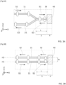
- FIGS. 14A, 14B illustrate a first embodiment of the projection system in which the lower electrode50 is positioned under the second level n2 of projection p2 and under the first level n1 of addressing a1. This makes it possible to limit or eliminate optical losses by absorption within the ITO.
- the addressing level a1 includes waveguides 11 typically subdivided via multimode interferometers MMI 60. According to one example, the light radiation is thus distributed in a balanced manner over a total of 4096 guides.
- the waveguides 11 open onto Bragg reflectors 41a.
- the projection level p2 comprises waveguides 21 partly directly above the waveguides 11 in the coupling portion 3.
- the waveguides 21 are attached to Bragg reflectors 42a.
- the Bragg reflectors 42a are superimposed along z on the Bragg reflectors 41a.
- the first embodiment of the projection system typically makes it possible to limit optical losses.
- the embodiments of the projection system illustrated in Figures 15A, 15B And 16A, 16B aim to reduce the voltage necessary to apply to the electrodes to extract the light radiation.
- the elements described and referenced for the first embodiment can also be transposed to the following two embodiments.
- FIGS. 15A, 15B illustrate a second embodiment of the projection system in which the lower electrode 50 is positioned between the second level n2 of projection p2 and the first level n1 of addressing a1.
- This makes it possible to bring the lower electrode 50 closer to the surface of the projector in the vicinity of which the counter electrode is located. The extraction tension is thus reduced.
- the separation distance ds between the first and second levels n1, n2 is increased. According to an example, ds ⁇ 850 nm.
- the coupling length of the coupling portion 3 is increased accordingly. This affects the compactness of the system.
- the second embodiment of the projection system typically allows moderate electrical consumption.
- FIGS. 16A, 16B illustrate a third embodiment of the projection system in which the lower electrode 50 is positioned at the same level as an intermediate level n1 designated ai.
- the lower electrode 50 is positioned above an addressing level a0, and below the projection level p2.
- the addressing level a0 comprises waveguides 31 without reflectors.
- the intermediate level ai includes waveguides 11 opening onto Bragg reflectors 41a.
- the projection level p2 includes waveguides 12 attached to Bragg reflectors 42a.
- the light radiation is here injected into the waveguides 31 of the addressing level a0, in the direction S1. It is then injected by coupling 13 into the waveguides 11, in direction S1. It is then reflected and injected by coupling into the waveguides 21, in direction S2 as previously. It is then extracted from the projection level by applying a voltage between the extraction electrodes.
- the intermediate level ai makes it possible to make an optical bridge between the addressing level a0 and the projection level p2.
- the separation distance ds can for example be reduced to 450 nm. This makes it possible to drastically reduce the length of the coupling portions 13, 3.
- a finite element simulation of the natural modes FDE (Finite Difference Eigenmode) indicates that a coupling length Le for the coupling portion 3 of the order of 20, 6 ⁇ m is suitable.
- the compactness of the system is preserved.
- the guides 31 can be moved away from the lower electrode 50. This makes it possible to limit or eliminate optical losses by absorption.
- the guides 31 are also relatively further from the guides 21. This makes it possible to limit or eliminate optical losses by multilevel crossings.
- the optical losses for this third embodiment are comparable to those induced in the first embodiment.
- the extraction voltage is further reduced with this electrode positioning 50, compared to the first embodiment.
- the third mode of realization of the projection system is a good compromise allowing to combine low optical losses and moderate electrical consumption. Its implementation is more expensive than the implementations of the first and second embodiments.
- the Bragg mirrors 41a, 42a are associated respectively with the intermediate level ai and the projection level p2. Other associations or configurations are possible.
- the Bragg mirrors 41a, 42a can in particular be associated respectively with the addressing level a0 and with the intermediate level ai.
- FIG. 17 illustrates a photonic projector architecture comprising two addressing or routing levels a1, a2, and a projection level p3. This allows, from a few light sources (S), to address emission points distributed arbitrarily on the surface of a retinal projector whose guides 21 have "zigzag" shapes to give the points of broadcast a random distribution.
- S light sources
- the routing part includes waveguides 11, 12 respectively on two levels, to avoid guide crossings. This helps limit optical losses.
- the projection part is located on a third level.
- the retrocoupling device 3, 4 advantageously makes it possible to superimpose the projection level p3 on the addressing levels a1, a2.
- FIG. 18 illustrates a multilevel feedback device called RGB (acronym for “Red Green Blue”), comprising sublevels dedicated to light radiation of different wavelengths (for example red, green, blue).
- RGB acronym for “Red Green Blue”
- the waveguides 11R, 11V, 11B are typically located on different levels.
- the device further comprises waveguides 21R, 21V, 21B respectively configured to guide the first, second and third wavelengths ⁇ 1, ⁇ 2, ⁇ 3.
- the waveguides 21R, 21V, 21B are typically located on the same level, for example a projection level of an RGB projector.
- the different light rays guided by the waveguides 11R, 11V, 11B propagate by back-coupling in the waveguides 21R, 21V, 21B.
- the Z0 zone illustrated in Figure 18 corresponds to this feedback zone.
- the waveguides 11R, 21R configured to guide the wavelength ⁇ 1 are typically dimensioned differently from the waveguides 11V, 21V configured to guide the wavelength ⁇ 2, and differently from the waveguides 11B, 21B configured to guide the wavelength ⁇ 3.
- the retrocouplers are thus specific to the different wavelengths ⁇ 1, ⁇ 2, ⁇ 3.
- the guides 11R, 21R have a 3R coupling portion and a reflector 41R, 42R.
- the 11V, 21V guides have a 3V coupling portion and a 41V, 42V reflector.
- the guides 11B, 21B have a coupling portion 3B and a reflector 41B, 42B.
- the separation distance along z between the guides 11B, 21B is relatively smaller than the separation distance along z between the guides 11V, 21V, and the separation distance along z between the guides 11V, 21V is relatively smaller than the separation distance along z between the guides 11R, 21R.
- the addressing level a30 including the guides 11R is the deepest with respect to the projection level p2 including the guides 21R.
- the addressing level a10 including the guides 11B is the shallowest with respect to the projection level p2 including the guides 21B.
- the addressing levels a30, a20, a10 respectively have depths dp3, dp2, dp1 with respect to the projection level p2, such that dp3 > dp2 > dp1.
- the deepest addressing levels a30, a20 can use guide portions of intermediate depths to route the light radiation up to the projection level p2.
- the 11V guide of the addressing level a20 can first be coupled to a portion of the 111V guide of intermediate depth dpm1.
- a 12V vertical coupling bridge thus allows light radiation of wavelength ⁇ 2 to pass from the 11V guide to the 111V guide portion, then to be injected into the 21V guide by back-coupling via the 3V coupling portion and the 41V reflectors , 42V.
- the guide 11R of the addressing level a30 can first be coupled to a portion of guide 111R of intermediate depth dpm2.
- This guide portion 111R can also be coupled to a guide portion 112R of intermediate depth dpm3.
- Two vertical coupling bridges 12R, 13R thus allow light radiation of wavelength ⁇ 1 to pass from the guide 11R to the guide portion 112R, then to be injected into the guide 21R by back-coupling via the coupling portion 3R and the reflectors 41R, 42R.
- the different levels of guides and guide portions are thus easier to produce by depositing and structuring layers. successive.
Landscapes
- Physics & Mathematics (AREA)
- General Physics & Mathematics (AREA)
- Optics & Photonics (AREA)
- Engineering & Computer Science (AREA)
- Microelectronics & Electronic Packaging (AREA)
- Nonlinear Science (AREA)
- Chemical & Material Sciences (AREA)
- Crystallography & Structural Chemistry (AREA)
- Catching Or Destruction (AREA)
- Optical Couplings Of Light Guides (AREA)
- Optical Integrated Circuits (AREA)
Applications Claiming Priority (1)
| Application Number | Priority Date | Filing Date | Title |
|---|---|---|---|
| FR2213726A FR3143778B1 (fr) | 2022-12-19 | 2022-12-19 | Dispositif de rétro-propagation multiniveaux |
Publications (1)
| Publication Number | Publication Date |
|---|---|
| EP4390480A1 true EP4390480A1 (de) | 2024-06-26 |
Family
ID=86657210
Family Applications (1)
| Application Number | Title | Priority Date | Filing Date |
|---|---|---|---|
| EP23216207.3A Pending EP4390480A1 (de) | 2022-12-19 | 2023-12-13 | Mehrstufige rückausbreitungsvorrichtung |
Country Status (4)
| Country | Link |
|---|---|
| US (1) | US20240201441A1 (de) |
| EP (1) | EP4390480A1 (de) |
| CN (1) | CN118226583A (de) |
| FR (1) | FR3143778B1 (de) |
Citations (4)
| Publication number | Priority date | Publication date | Assignee | Title |
|---|---|---|---|---|
| US20200096779A1 (en) * | 2018-09-20 | 2020-03-26 | E Ink Corporation | Three dimensional display apparatus |
| EP3945365A1 (de) * | 2020-07-29 | 2022-02-02 | Facebook Technologies, LLC | Wellenleiterbasierter projektor |
| WO2022098709A1 (en) * | 2020-11-06 | 2022-05-12 | Facebook Technologies, Llc | Slab waveguide and projector with intermodal coupling |
| WO2022120250A1 (en) * | 2020-12-04 | 2022-06-09 | Facebook Technologies, Llc | Patterned backlight for display panel |
Family Cites Families (6)
| Publication number | Priority date | Publication date | Assignee | Title |
|---|---|---|---|---|
| JP3257510B2 (ja) * | 1998-05-29 | 2002-02-18 | 日本電気株式会社 | 光デバイス |
| US6813405B1 (en) * | 2002-03-29 | 2004-11-02 | Teem Photonics | Compact apparatus and method for integrated photonic devices having folded directional couplers |
| US8200051B2 (en) * | 2008-03-24 | 2012-06-12 | Nitto Denko Corporation | Apparatus using waveguide, optical touch panel, and method of fabricating waveguide |
| CN107533255A (zh) * | 2015-04-23 | 2018-01-02 | 镭亚股份有限公司 | 基于双光导光栅的背光以及使用该背光的电子显示器 |
| WO2019043917A1 (ja) * | 2017-09-01 | 2019-03-07 | 三菱電機株式会社 | レーザ装置 |
| FR3106669B1 (fr) * | 2020-01-24 | 2022-08-05 | Commissariat Energie Atomique | Dispositif de projection distribuée de lumière |
-
2022
- 2022-12-19 FR FR2213726A patent/FR3143778B1/fr active Active
-
2023
- 2023-12-13 EP EP23216207.3A patent/EP4390480A1/de active Pending
- 2023-12-15 US US18/541,198 patent/US20240201441A1/en active Pending
- 2023-12-18 CN CN202311739062.XA patent/CN118226583A/zh active Pending
Patent Citations (4)
| Publication number | Priority date | Publication date | Assignee | Title |
|---|---|---|---|---|
| US20200096779A1 (en) * | 2018-09-20 | 2020-03-26 | E Ink Corporation | Three dimensional display apparatus |
| EP3945365A1 (de) * | 2020-07-29 | 2022-02-02 | Facebook Technologies, LLC | Wellenleiterbasierter projektor |
| WO2022098709A1 (en) * | 2020-11-06 | 2022-05-12 | Facebook Technologies, Llc | Slab waveguide and projector with intermodal coupling |
| WO2022120250A1 (en) * | 2020-12-04 | 2022-06-09 | Facebook Technologies, Llc | Patterned backlight for display panel |
Non-Patent Citations (1)
| Title |
|---|
| MARTINEZ CHRISTOPHE ET AL: "See-through holographic retinal projection display concept", vol. 5, no. 10, 20 October 2018 (2018-10-20), US, pages 1200, XP055942106, ISSN: 2334-2536, Retrieved from the Internet <URL:http://dx.doi.org/10.1364/OPTICA.5.001200> DOI: 10.1364/OPTICA.5.001200 * |
Also Published As
| Publication number | Publication date |
|---|---|
| FR3143778A1 (fr) | 2024-06-21 |
| US20240201441A1 (en) | 2024-06-20 |
| CN118226583A (zh) | 2024-06-21 |
| FR3143778B1 (fr) | 2024-12-13 |
Similar Documents
| Publication | Publication Date | Title |
|---|---|---|
| EP3610309B1 (de) | Photonischer chip mit integrierter kollimationsstruktur | |
| EP3540878B1 (de) | Photonenvorrichtung, die einen laser umfasst, der optisch mit einem silizium-wellenleiter verbunden ist, und herstellungsverfahren einer solchen photonenvorrichtung | |
| EP3495861B1 (de) | Photonen-chip mit rückfaltung des lichtwegs und integrierter bündelungsstruktur | |
| EP3521879A1 (de) | Photonischer chip mit integrierter kollimationsstruktur | |
| EP3579028B1 (de) | Bildsensoren mit einer matrix von interferenzfiltern | |
| EP3607585B1 (de) | Vorrichtung und verfahren zur multispektralen bildgebung im infrarotbereich | |
| FR3060772A1 (fr) | Circuit photonique integre optimise | |
| WO2003044579A2 (fr) | Structure a cristal photonique pour la conversion de mode | |
| EP2286289A2 (de) | Vorrichtung zum kuppeln einer glasfaser und einer nanophotonischen komponente | |
| CA2291522A1 (fr) | Modulateur de phase a semi-conducteur | |
| FR2570839A1 (fr) | Dispositif de couplage entre des guides d'onde, monolithiquement integre avec ceux-ci sur un substrat semiconducteur | |
| FR3051561A1 (fr) | Dispositif photonique integre a couplage optique ameliore | |
| EP2510391B1 (de) | Vorrichtung zur kopplung einer elektromagnetischen welle zwischen einem wellenleiter und einer gerillten metallführung, verfahren zur herstellung dieser vorrichtung und optischer elektrischer koppler für ein objekt mit der optischen kopplungsvorrichtung | |
| EP3855068B1 (de) | Vorrichtung zur verteilten lichtprojektion | |
| EP4009456B1 (de) | Verfahren zur herstellung eines verteilten bragg-spiegels | |
| EP2614526A1 (de) | Lichtdetektor und zugehörige detektionsmatrix | |
| EP4390480A1 (de) | Mehrstufige rückausbreitungsvorrichtung | |
| EP3968064A1 (de) | Optische filtervorrichtung | |
| WO1999064905A1 (fr) | Dispositif de diffraction de lumiere enfoui dans un materiau | |
| EP3814814B1 (de) | Spektralfilter mit mindestens zwei gekoppelten fabry-perot-strukturen | |
| FR2685096A1 (fr) | Miroir optique integre et son procede de fabrication. | |
| EP4034923B1 (de) | Optisches system und verfahren zu dessen herstellung | |
| EP4707884A1 (de) | Photonische integrierte schaltung | |
| WO2024052607A1 (fr) | Filtre spectral a resonateurs couples | |
| EP4528337A2 (de) | Multispektraler filter für elektromagnetische strahlung und verfahren zu seiner herstellung |
Legal Events
| Date | Code | Title | Description |
|---|---|---|---|
| PUAI | Public reference made under article 153(3) epc to a published international application that has entered the european phase |
Free format text: ORIGINAL CODE: 0009012 |
|
| STAA | Information on the status of an ep patent application or granted ep patent |
Free format text: STATUS: REQUEST FOR EXAMINATION WAS MADE |
|
| 17P | Request for examination filed |
Effective date: 20231213 |
|
| AK | Designated contracting states |
Kind code of ref document: A1 Designated state(s): AL AT BE BG CH CY CZ DE DK EE ES FI FR GB GR HR HU IE IS IT LI LT LU LV MC ME MK MT NL NO PL PT RO RS SE SI SK SM TR |
|
| RAP3 | Party data changed (applicant data changed or rights of an application transferred) |
Owner name: COMMISSARIAT A L'ENERGIE ATOMIQUE ET AUX ENERGIESALTERNATIVES |