EP4390623B1 - Mikroelektromechanische sensorvorrichtung mit verbesserter verwaltung eines abschaltzustands - Google Patents
Mikroelektromechanische sensorvorrichtung mit verbesserter verwaltung eines abschaltzustands Download PDFInfo
- Publication number
- EP4390623B1 EP4390623B1 EP23213652.3A EP23213652A EP4390623B1 EP 4390623 B1 EP4390623 B1 EP 4390623B1 EP 23213652 A EP23213652 A EP 23213652A EP 4390623 B1 EP4390623 B1 EP 4390623B1
- Authority
- EP
- European Patent Office
- Prior art keywords
- power
- sensor device
- voltage
- microelectromechanical sensor
- power supply
- Prior art date
- Legal status (The legal status is an assumption and is not a legal conclusion. Google has not performed a legal analysis and makes no representation as to the accuracy of the status listed.)
- Active
Links
Images


Classifications
-
- G—PHYSICS
- G06—COMPUTING OR CALCULATING; COUNTING
- G06F—ELECTRIC DIGITAL DATA PROCESSING
- G06F1/00—Details not covered by groups G06F3/00 - G06F13/00 and G06F21/00
- G06F1/26—Power supply means, e.g. regulation thereof
- G06F1/32—Means for saving power
- G06F1/3203—Power management, i.e. event-based initiation of a power-saving mode
- G06F1/3234—Power saving characterised by the action undertaken
- G06F1/3287—Power saving characterised by the action undertaken by switching off individual functional units in the computer system
-
- G—PHYSICS
- G01—MEASURING; TESTING
- G01D—MEASURING NOT SPECIALLY ADAPTED FOR A SPECIFIC VARIABLE; ARRANGEMENTS FOR MEASURING TWO OR MORE VARIABLES NOT COVERED IN A SINGLE OTHER SUBCLASS; TARIFF METERING APPARATUS; MEASURING OR TESTING NOT OTHERWISE PROVIDED FOR
- G01D3/00—Indicating or recording apparatus with provision for the special purposes referred to in the subgroups
- G01D3/028—Indicating or recording apparatus with provision for the special purposes referred to in the subgroups mitigating undesired influences, e.g. temperature, pressure
- G01D3/036—Indicating or recording apparatus with provision for the special purposes referred to in the subgroups mitigating undesired influences, e.g. temperature, pressure on measuring arrangements themselves
-
- B—PERFORMING OPERATIONS; TRANSPORTING
- B81—MICROSTRUCTURAL TECHNOLOGY
- B81B—MICROSTRUCTURAL DEVICES OR SYSTEMS, e.g. MICROMECHANICAL DEVICES
- B81B7/00—Microstructural systems ; Auxiliary parts of microstructural devices or systems
- B81B7/008—MEMS characterised by an electronic circuit specially adapted for controlling or driving the same
-
- G—PHYSICS
- G01—MEASURING; TESTING
- G01C—MEASURING DISTANCES, LEVELS OR BEARINGS; SURVEYING; NAVIGATION; GYROSCOPIC INSTRUMENTS; PHOTOGRAMMETRY OR VIDEOGRAMMETRY
- G01C19/00—Gyroscopes; Turn-sensitive devices using vibrating masses; Turn-sensitive devices without moving masses; Measuring angular rate using gyroscopic effects
- G01C19/56—Turn-sensitive devices using vibrating masses, e.g. vibratory angular rate sensors based on Coriolis forces
-
- G—PHYSICS
- G05—CONTROLLING; REGULATING
- G05F—SYSTEMS FOR REGULATING ELECTRIC OR MAGNETIC VARIABLES
- G05F1/00—Automatic systems in which deviations of an electric quantity from one or more predetermined values are detected at the output of the system and fed back to a device within the system to restore the detected quantity to its predetermined value or values, i.e. retroactive systems
- G05F1/10—Regulating voltage or current
- G05F1/46—Regulating voltage or current wherein the variable actually regulated by the final control device is DC
-
- B—PERFORMING OPERATIONS; TRANSPORTING
- B81—MICROSTRUCTURAL TECHNOLOGY
- B81B—MICROSTRUCTURAL DEVICES OR SYSTEMS, e.g. MICROMECHANICAL DEVICES
- B81B2207/00—Microstructural systems or auxiliary parts thereof
- B81B2207/03—Electronic circuits for micromechanical devices which are not application specific, e.g. for controlling, power supplying, testing, protecting
Definitions
- the present invention relates to a microelectromechanical sensor (MEMS) device, with improved management of a power-down condition.
- MEMS microelectromechanical sensor
- MEMS sensor devices In a known manner, there are several applications of MEMS sensor devices, defined as "ultra low power” applications, where an extremely low power consumption is required, for example in wearable or hearable apparatuses, such as electronic watches or bands or bracelets, earphones, smart contact lenses, smart pens or the like.
- MEMS sensor devices One problem affecting MEMS sensor devices in such applications is represented by the power consumption while in power-on but inactive state (i.e., which occurs when the same sensor devices are not in the operating phase, for acquisition and possible processing of data associated with one or more quantities to be detected).
- MEMS sensor devices such as for example accelerometers, gyroscopes, pressure sensors, etc.
- ASIC Application Specific Integrated Circuit
- a solution that has been proposed to reduce power consumption provides for a so-called multi-domain (or multi-voltage) approach according to which the aforementioned electronic circuitry is divided into a certain number of separate domains (or independent portions), each of which may be selectively powered, even at different voltages, such as to have the possibility of switching-off (deactivating) one or more of these domains, with a resulting power saving in the power-down condition.
- a digital or logic part of the aforementioned electronic circuitry is usually powered with a lower voltage with respect to the power supply voltage provided from the outside (for example from a battery), using voltage regulators that allow an under-regulated voltage to be generated starting from the external power supply voltage.
- the aforementioned multi-domain approach requires the use of power supply switches, associated with the aforementioned domains and controlled to selectively activate/deactivate the provision of the respective power supply voltage to the respective domains.
- These power supply switches may be implemented externally to the MEMS sensor devices, with a consequent increase in the circuit complexity and in the size occupation and also with a control burden by the external processor (application or host processor) of the electronic apparatus wherein the same MEMS sensor devices are housed.
- the same power supply switches may alternatively be implemented in an embedded manner within the MEMS sensor devices, in the corresponding electronic circuitry.
- control logic that controls switching of these power supply switches which is implemented in the digital part of the electronic circuitry, is required to be always powered, even in the power-down condition, with a resulting power consumption which may not be negligible, in particular due to the aforementioned voltage regulator (which provides the under-regulated power supply voltage to the digital part).
- the aim of the present solution is to solve, at least in part, the previously highlighted problems and to meet the aforementioned requirement.
- an aspect of the present solution provides for implementing, in the electronic circuitry of a microelectromechanical sensor (MEMS) device, at least two different and distinct voltage domains (i.e. distinct portions powered at different voltages): a first domain, which defines an always-on core in the presence of an external power supply voltage (provided from outside of the microelectromechanical sensor device), powered by the same external power supply voltage; and at least one second domain, powered by a voltage regulator at a voltage that is different from, in particular lower than, the external power supply voltage, selectively switchable into an on- or off- condition by the aforementioned always-on core.
- MEMS microelectromechanical sensor
- a so-called deep power-down condition is implemented, in the microelectromechanical sensor device, by powering off the voltage regulator and the voltage domains associated therewith, in particular the aforementioned second domain.
- the power consumption is extremely low (of the order of at most a few tens of nA), being associated only with the electrical consumption of the aforementioned always-on core.
- the complete functions of the microelectromechanical sensor device are not available (e.g., a maximum operating frequency is not available and reading/writing operations are not allowed, except for a dedicated wake-up sequence, as will be discussed in detail in the following).
- This always-on core is also configured to manage the transition between the aforementioned deep power-down condition and a different power-down condition, defined here as a soft power-down condition, during which the aforementioned voltage regulator is powered on.
- the circuit stages of the microelectromechanical sensor device are switchable to the inactive state in order to reduce the corresponding power consumption, by a switching control logic powered by the aforementioned voltage regulator.
- one or more (typically most) of the circuit stages of the microelectromechanical sensor device are switched to the inactive state by the switching control logic, so as to reduce the power consumption of the same microelectromechanical sensor device.
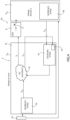
- Figure 1 schematically shows the architecture of a microelectromechanical sensor device 1, according to an embodiment of the present solution.
- the microelectromechanical sensor device 1 comprises a micromechanical detection structure (of a known type, here not illustrated), configured to sense one or more detection quantities; and an electronic circuitry 2, operatively coupled to the micromechanical detection structure and configured to receive and process the aforementioned detection quantity.
- the electronic circuitry 2 comprises a digital part 2a and an analog part 2b.
- the digital part 2a comprises, as will be evident to a person skilled in the art, logic or digital elements such as registers, timing elements, logic gates and processing modules for performing a set of logic operations (in particular in the form of algorithms); in a possible implementation, this digital part 2a may comprise a processing unit, such as a microcontroller, a microprocessor or a similar embedded digital processing unit.
- logic or digital elements such as registers, timing elements, logic gates and processing modules for performing a set of logic operations (in particular in the form of algorithms); in a possible implementation, this digital part 2a may comprise a processing unit, such as a microcontroller, a microprocessor or a similar embedded digital processing unit.
- the electronic circuitry 2 is configured to receive from outside the microelectromechanical sensor device 1, for example from a battery (not illustrated here) of an electronic apparatus, in particular of the portable or wearable type, where the same microelectromechanical sensor device 1 is used, an external power supply voltage V DD , for example comprised between 1.71 V and 3.6 V.
- V DD external power supply voltage
- the digital part 2a comprises a first voltage domain 4, powered by the external power supply voltage V DD ; and at least one second voltage domain 6, separate and distinct from the first voltage domain 4, powered by a regulated voltage V REG , having a lower value than the external power supply voltage V DD , for example equal to 1.2 V.
- this regulated voltage V REG is generated by a voltage regulator 8, for example of the LDO (Low DropOut) type.
- the analog part 2b of the electronic circuitry 2 may also be powered by the aforementioned external power supply voltage V DD .
- the first voltage domain 4 comprises an always-on core 10, which includes a control logic of very low complexity and small dimensions (for example a few tens of thousands of square microns), configured to manage the electric power supply mode of the microelectromechanical sensor device 1 and in particular the transition between the aforementioned deep power-down and soft power-down conditions.
- a control logic of very low complexity and small dimensions (for example a few tens of thousands of square microns), configured to manage the electric power supply mode of the microelectromechanical sensor device 1 and in particular the transition between the aforementioned deep power-down and soft power-down conditions.
- the second voltage domain 6 comprises digital resources powered by the aforementioned regulated voltage V REG , which in turn may be divided into multiple sub-domains 12, distinct from each other and selectively controllable in power-on or in power-off, as shown schematically through power supply switching elements 13, by a switching control logic 15 (also powered by the aforementioned regulated voltage V REG ).
- This switching control logic 15, which is part of the above second voltage domain 6, for example is configured to receive from the outside (for example from an application, or host, processor of the electronic apparatus wherein the microelectromechanical sensor device 1 is used) and decode suitable commands to manage power-on of the aforementioned sub-domains 12.
- a main sub-domain (sub-domain 1) is present, wherein the aforementioned switching control logic 15 and a number of secondary sub-domains (in the example sub-domain 2 and sub-domain 3) are implemented.
- this second voltage domain 6 comprises all the digital resources of the digital part 2a of the electronic circuitry 2, except for the (minimum) resources dedicated to the implementation of the aforementioned always-on core 10 in the first voltage domain 4.
- the always-on core 10 is configured to control switching-off or switching-on of the voltage regulator 8 by means of a control signal S C generated by the same always-on core 10 and provided to the voltage regulator 8; schematically, Figure 1 shows a power-on switch 17, which is controlled by the aforementioned control signal S C to switch-off (for example, with a high value of the control signal S C ) or switch-on (for example, with a low value of the control signal S C ) the voltage regulator 8, disabling or enabling generation of the regulated voltage V REG .
- the voltage regulator 8, and, consequently, the second voltage domain 6 (and the corresponding sub-domains 12), are powered off, deactivated, so as to minimize power consumption.
- the power consumption of the electronic circuitry 2 is substantially due only to the always-on core 10 (being the second voltage domain 6 not powered), which, as indicated, comprises only the minimum control logic to manage power-on of the voltage regulator 8. The power consumption in deep power-down condition is therefore very small.
- the always-on core 10 is configured to manage the transition from the deep power-down condition to the soft power-down condition as a function of a first control signal S PD1 received from the outside (for example from the application, or host, processor of the electronic apparatus in which the microelectromechanical sensor device 1 is used), at an input/output element (pad or pin) 18 of the microelectromechanical sensor device 1.
- a first control signal S PD1 received from the outside (for example from the application, or host, processor of the electronic apparatus in which the microelectromechanical sensor device 1 is used), at an input/output element (pad or pin) 18 of the microelectromechanical sensor device 1.
- the always-on core 10 causes power-on of the voltage regulator 8 and activation of the second voltage domain 6, to exit from the deep power-down condition and, initially, for the implementation of the soft power-down condition.
- the always-on core 10 is also configured to receive a second control signal S PD2 , as a function of which, as will be discussed in detail below, causes power-off of the voltage regulator 8 and deactivation of the second voltage domain 6, for the implementation of the deep power-down condition.
- the always-on core 10 receives this second control signal S PD2 (again from outside of the microelectromechanical sensor device 1) via the second voltage domain 6, which is also coupled to the input/output element 18 of the microelectromechanical sensor device 1.
- step 20 upon power-on of the microelectromechanical sensor device 1 (i.e., when the external power supply voltage V DD is provided, for example following an enable command generated by the application or host processor), the same microelectromechanical sensor device 1 is configured to automatically enter the deep power down (deep PD) condition, step 21, with the voltage regulator 8 which is powered off and therefore does not provide power supply to the second voltage domain 6 (essentially, the power-on switch 17 of Figure 1 is open).
- the voltage regulator 8 which is powered off and therefore does not provide power supply to the second voltage domain 6 (essentially, the power-on switch 17 of Figure 1 is open).
- the always-on core 10 powers on the voltage regulator 8 and enable supply of the regulated voltage V REG for powering the second voltage domain 6 (the power-on switch 17 is closed).
- step 22 in the same second voltage domain 6, preliminary operations are performed for retrieval of configuration and trimming information from a non-reprogrammable internal memory (or read-only memory, of the OTP - One Time Programmable - type), which are stored in volatile memory registers, to carry out the so-called "boot” or restore of the microelectromechanical sensor device 1.
- a non-reprogrammable internal memory or read-only memory, of the OTP - One Time Programmable - type
- the microelectromechanical sensor device 1 then enters the soft power down (soft PD) condition, as shown in step 23.
- deactivation of (typically most of) the respective sub-domains 12 may be managed in this condition to reduce a power consumption of the microelectromechanical sensor device 1 (as previously indicated, the switching control logic 15 may receive and decode suitable commands received for this purpose from the outside, for example from the aforementioned application processor, at the input/output element 18).
- the same microelectromechanical sensor device 1 may enter an operative or active (ON) condition, shown in step 24, in which the complete functionalities are ensured, for acquisition and processing of data (corresponding to the quantity to be sensed) at a desired ODR - Output Data Rate. Moreover, in this active condition the maximum operating frequency is available for the microelectromechanical sensor device 1 and reading/writing operations are entirely allowed.
- ON operative or active
- the switching control logic 15 in the second voltage domain 6 may control for this purpose one or more of the power supply switching elements 13 to activate the respective sub-domains 12 and thus ensure the corresponding operativeness.
- the switching control logic 15 may control for this purpose one or more of the power supply switching elements 13 to activate the respective sub-domains 12 and thus ensure the corresponding operativeness.
- most (for example more than half) of the above sub-domains 12 are activated by the switching control logic 15.
- the microelectromechanical sensor device 1 may return to the soft power down condition, step 23 (in which the switching control logic 15 may again interrupt the power supply of one or more of the aforementioned sub-domains 12).
- the microelectromechanical sensor device 1 may be returned into the deep power down condition, step 21.
- the sub-domains 12 are powered off (if they were still on) and then the always-on core 10 again powers off the voltage regulator 8, interrupting electrical power supply to the aforementioned second voltage domain 6 .
- the deep power down condition is immediately activated; exit from this deep power down condition then occurs at the arrival of the dedicated wake-up sequence (as indicated by the arrow).
- This dedicated wake-up sequence entails in particular power-on of the voltage regulator 8 (the control signal S C goes to the low state) and subsequent enabling of the regulated voltage V REG generated by the same voltage regulator 8.
- the microelectromechanical sensor device 1 At the end of the consequent restore operations (BOOT), the microelectromechanical sensor device 1 enters the soft power down condition, which will then evolve into the normal operativeness of the same device or, alternatively, again into the deep power down condition (in the manner previously described and not illustrated in the aforementioned Figure 3 ).
- the always-on core 10 comprises an interface stage 30, coupled to the input/output element 18 of the microelectromechanical sensor device 1 to receive the aforementioned first control signal S PD1 .
- this interface stage 30 implements a serial interface, of the I2C(I3C)/SPI type; and the input/output element 18 is coupled to a serial bus interposed between the application or host processor and the microelectromechanical sensor device 1.
- the always-on core 10 further comprises: a soft power-down procedure stage 32, having a first input coupled to the interface stage 30 and also a second input; and a coupling stage 34, interposed between the second voltage domain 6 and the same soft power-down procedure stage 32, having a respective input coupled to the second voltage domain 6 and an output coupled to the second input of the soft power-down procedure stage 32.
- This coupling stage 34 in a manner not illustrated in detail, comprises level shifter and/or synchronization elements, configured to put in communication the first and second voltage domains 4, 6, which work at different voltages and are not synchronized with each other. Isolation cells 34' are also present at the input of the coupling stage 34, in order to isolate, under certain operating conditions, the first voltage domain 4 from the second voltage domain 6.
- the soft power-down procedure stage 32 is configured to receive, at the first input, the first control signal S PD1 , as a function of which it enables the voltage regulator 8, through the control signal S C . As a function of the same first control signal S PD1 , the soft power-down procedure stage 32 also generates a control signal S ISO to disable the isolation cells 34' of the coupling stage 34 (which are, in fact, active during the deep power down condition).
- the first control signal S PD1 carries the aforementioned wake-up sequence, which determines the transition between the deep and soft power-down conditions.
- the first control signal S PD1 may entail writing a dedicated wake-up bit, using a standard-type SPI writing operation, for example performed at a clock frequency of 10 MHz.
- a high logic value '1' of the aforementioned wake-up bit may determine wake-up from the deep power down condition.
- the first control signal S PD1 may assume the following sequence: Start + Static Address + Nack, for the aforementioned wake-up from the deep power down condition.
- the command for maintaining the deep power down condition may be, in both cases, a wake-up bit (similarly, the first control signal S PD1 ) set to low logic level '0'.
- the same soft power-down procedure stage 32 is configured to receive, at the second input, the second control signal S PD2 , coming from the second voltage domain 6 through the coupling stage 34.
- the aforementioned second voltage domain 6 has a respective interface stage 38, for example of the I2C(I3C)/SPI serial type, which is coupled to the input/output element 18 (and to the corresponding serial bus), to receive from the outside, for example from the application or host processor, the aforementioned power-down or sleep command, which determines the return to the deep power down condition.
- a respective interface stage 38 for example of the I2C(I3C)/SPI serial type, which is coupled to the input/output element 18 (and to the corresponding serial bus), to receive from the outside, for example from the application or host processor, the aforementioned power-down or sleep command, which determines the return to the deep power down condition.
- the soft power-down procedure stage 32 enables again the isolation cells 34' of the coupling stage 34 (through the aforementioned control signal S ISO ) and also deactivates the voltage regulator 8 (through the aforementioned control signal S C ).
- the always-on core 10 has functionalities reduced to a minimum, to minimize area and consumption and leakage currents thereof during the deep power down condition.
- the aforementioned interface stage 30 is configured to recognize only the first control signal S PD1 ; the second control signal S PD2 is in fact received and recognized by the respective interface stage 38 of the second voltage domain 6.
- the interface stage 30 of the always-on core 10 implements a slave interface (in the example of the I2C, I3C or SPI serial type) with reduced functionality, in particular with only the ability to write in an internal register as a function of the aforementioned first control signal S PD1 received from the outside, so as not to degrade the performances of the interface timings, which are more critical during reading operations.
- the same interface stage 30 of the always-on core 10 is not able to perform any other writing operation, nor any reading operation.
- This possibility may be advantageous, for example in order to maintain a compatibility of the microelectromechanical sensor device 1 with electronic apparatuses (and corresponding application or host processors) which do not provide (or are not programmable) for management of the transition between the aforementioned deep and soft power down conditions.
- the always-on core 10 further comprises a bypass stage 40, interposed between the interface stage 30 and the soft power-down procedure stage 32 and configured to receive a configuration signal S conf .
- the bypass stage 40 may inhibit the implementation of the deep power down condition upon powering on the microelectromechanical sensor device 1, as a function of the aforementioned configuration signal S conf , the value of which may be set to configure the (soft or deep) power down condition which is implemented upon powering on the same microelectromechanical sensor device 1.
- the bypass stage 40 is configured to bypass (inhibit) the aforementioned first power-down control signal S PD1 received at the input/output element 18, which is required, as previously discussed for the transition from the deep power down to the soft power down condition; and to automatically enable (i.e., without requesting a command by the user or the application or host processor) the soft power down condition upon powering on the microelectromechanical sensor device 1.
- the bypass stage 40 is configured to be substantially transparent as regards the operation of the always-on core 10, whose operation thus corresponds to what has been previously illustrated (in particular, with the microelectromechanical sensor device 1 which automatically enters the deep power down condition upon power-on and with the need to receive the aforementioned first power-down control signal S PD1 for the transition to the soft power down condition).
- the configuration signal S conf is stored in the second voltage domain 6 in an internal non-reprogrammable read-only memory (of the OTP type), denoted with 37, and is received in the first voltage domain 4 from the second voltage domain 6 via the coupling stage 34.
- This configuration signal S conf is in the example a configuration bit written in the memory, for example of the OTP type, during factory calibration of the microelectromechanical sensor device 1.
- step 41 an automatic wake-up sequence is implemented, first retrieving, for example from the internal non-reprogrammable read-only memory 37, the value of the configuration signal S conf , step 42.
- This value has been programmed for example in the factory calibration step during testing of the microelectromechanical sensor device 1.
- step 42 the preliminary "boot” or restore operations are also performed, with the retrieval of configuration and trimming information of the microelectromechanical sensor device 1.
- step 43 operation upon power-on is similar to what has been previously described, with the device entering the deep power down condition, step 43, and with the always-on core 10 waiting for the dedicated wake-up command, represented by the first control signal S PD1 received from the outside, required to enter the soft power down condition, step 44.
- the device In the event that the configuration signal S conf has instead a low logic value, the device automatically enters the soft power down condition, aforementioned step 44 (thus bypassing the deep power down condition).
- the microelectromechanical sensor device 1 may enter the active or ON condition, shown in step 45, wherein the complete functionalities are ensured, for example for data acquisition and processing.
- the microelectromechanical sensor device 1 may return to the soft power down condition, step 44. Furthermore, from the same soft power down condition, or from the active condition, the microelectromechanical sensor device 1 may be returned to the deep power down condition, step 43, after receiving the dedicated power-down or sleep command, represented by the second control signal S PD2 .
- Figure 7A refers to the case in which the configuration signal S conf (for example, the corresponding OTP memory bit) has a low logic value and, at the end of the aforementioned automatic power-on sequence, the microelectromechanical sensor device 1 automatically enters the soft power down condition (thus bypassing the deep power down condition).
- the configuration signal S conf for example, the corresponding OTP memory bit
- the voltage regulator 8 After enabling the external power supply voltage V DD (with the power-on reset signal POR_VDD going to the high state), in this case the voltage regulator 8 is immediately powered on (the control signal S C goes to the low state) for subsequent enabling of the regulated voltage V REG generated by the same voltage regulator 8.
- the soft power down condition is automatically enabled.
- the configuration signal S conf has a high logic value and, at the end of the aforementioned automatic power-on sequence, the microelectromechanical sensor device 1 automatically enters the deep power down condition.
- the voltage regulator 8 is immediately powered on to enable the regulated voltage V REG and to execute the restore operation.
- the value of the configuration signal S conf is such as to automatically enable the deep power down condition, whereby, after the aforementioned restore operation, the voltage regulator 8 is powered off and the regulated voltage V REG is inhibited.
- this bypass stage 40 comprises a multiplexer element 50, having a first signal input 50a, which receives an automatic-enabling command; a second signal input 50b, which receives the aforementioned first control signal S PD1 from the interface stage 30; and a selection input 50c.
- this automatic-enabling command has a value such as to automatically enable the soft power-down procedure stage 32; in the example discussed, this value corresponds to a high logic value '1'.
- the bypass stage 40 also comprises a logic module 52, which receives at an input the aforementioned configuration signal S conf from the coupling stage 34 and is configured to generate, as a function of the same configuration signal S conf , a selection signal S SEL for the selection input 50c of the multiplexer element 50.
- this logic module 52 comprises a first and a second clocking gate cells 54, 55 (i.e., for selective supply of a timing signal).
- the first clocking gate cell 54 has an enable input (indicated by E) coupled to the output of the coupling stage 34.
- This first clocking gate cell 54 thus receives the configuration signal S conf and selectively provides at an output (indicated by G), as a function of the value of this configuration signal S conf , a clock signal, CK, received at input.
- This clock signal CK is generated by a system oscillator, for example operating at 40kHz, of the microelectromechanical sensor device 1 and determines the timing of the digital part 2a of the electronic circuitry 2 of the same microelectromechanical sensor device 1.
- the second clocking gate cell 55 receives a gating signal S G at a respective enable input and selectively provides at an output, as a function of the value of this gating signal S G , the clock signal CK received at input.
- the logic module 52 also comprises a first and a second sequential memory elements 56, 57, cascade-connected to each other, in particular D-type flip-flops with clear and, respectively, set asynchronous inputs receiving the aforementioned power-on reset signal POR_VDD.
- the first sequential memory element 56 has a clock input connected to the output of the first clocking gate cell 54, a D input receiving a high logic value ('1') and a clear asynchronous input (CR) receiving the aforementioned power-on reset signal POR_VDD.
- the second sequential memory element 57 has a clock input connected to the output of the second clocking gate cell 55, a D input connected to the Q output of the first sequential memory element 56 and a set asynchronous input (S) receiving the aforementioned power-on reset signal POR_VDD.
- the Q output of this second sequential memory element 57 provides the aforementioned selection signal S SEL for the selection input 50c of the multiplexer element 50.
- the logic module 52 further comprises: a counter element 58, receiving the clock signal CK and the power-on reset signal POR_VDD and generating a count signal at the output; and a combinatorial logic block 59, which receives this count signal from the counter element 58 and also the configuration signal S conf from the coupling stage 34 and, based on these signals, generates the aforementioned gating signal S G for the second clocking gate cell 55.
- the always-on core 10 is powered by the external voltage V DD and the power-on reset signal POR_VDD rises with the power supply, reaching the high logic value '1', when power supply becomes stable.
- the second sequential memory element 57 has the Q output at '1' due to the power-on reset signal POR_VDD (provided to the set input), while the first sequential memory element 56 has the Q output at '0', again due to the power-on reset signal POR_VDD (in this case provided to the clear input).
- the output of the second sequential memory element 57 provides the selection signal S SEL for the selection input 50c of the multiplexer element 50.
- the high logic value of this selection signal S SEL is maintained until the power-on reset action is finished, in order to avoid that the soft power-down procedure may start before the power supply has become stable.
- the second clocking gate cell 55 is enabled by the counter element 58 (which has reached the end of the count); consequently, the logic '0' on the Q output of the first sequential memory element 56 is transferred ("re-latched") onto the second sequential memory element 57, thereby modifying to the low logic value the selection signal S SEL for the multiplexer element 50.
- This low logic value couples the first signal input 50a to the output, allowing the automatic-enabling command (having a high logic value '1') to pass to the output.
- the wake-up command decoded by the interface stage 30 (the first control signal S PD1 ) is bypassed and the soft power-down procedure stage 32 is enabled to automatically implement the soft power-down procedure, which provides for the power-on of the voltage regulator 8 and the power supply of the second voltage domain 6.
- the automatic power-on sequence provides for retrieval of the configuration and trimming information from the internal non-reprogrammable memory (OTP), among which the bit of the aforementioned configuration signal S conf is also present.
- OTP internal non-reprogrammable memory
- This bit is transferred through the coupling stage 34 (and the corresponding level and synchronization shifter elements) from the second voltage domain 6 to the first voltage domain 4.
- this configuration signal S conf is low ('0')
- the combinatorial logic block 59 of the logic module 52 is not activated and the soft power down condition is therefore maintained (which may subsequently evolve, as discussed, into the normal or data acquisition condition).
- this configuration signal S conf is high ('1')
- the combinatorial logic block 59 is activated and the first clocking gate cell 54 is enabled.
- the logic value '1' on the D input of the first sequential memory element 56 is then transferred first to the D input and then to the Q output of the second sequential memory element 57, thereby modifying to the high logic value the value of the selection signal S SEL for the multiplexer element 50.
- This high logic value couples the second input 50b of the multiplexer element 50 to the output, so that the first control signal S PD1 coming from the interface stage 30 is allowed to pass towards the output.
- This first control signal S PD1 is initially at the low logic value, since there has been no wake-up command by the user or from the application or host processor.
- the soft power-down procedure stage 32 not receiving the decoding of a wake-up command, disables the voltage regulator 8 causing the system to enter the deep power down condition, waiting to receive the aforementioned wake-up command (through the first command signal S PD1 , as previously discussed in detail).
- Tests and simulations carried out by the Applicant have, for example, shown the possibility of obtaining a power consumption in deep power down condition of the order of a few tens of nA (for example around 20nA), as compared to a consumption in a soft power down condition of some ⁇ A (for example about 2 ⁇ A), therefore two orders of magnitude lower.
- the solution described provides for an automatic approach that does not require any additional intervention by the user or the host application, as regards management of power supply domains.
- the same solution is advantageously completely embedded in the microelectromechanical sensor device 1, without requiring elements external to the same microelectromechanical sensor device 1, for example power supply management switches.
- the embodiment which envisages the presence of the bypass stage 40 in the always-on core 10 is advantageous, allowing the possibility of configuring the power-down condition management mode (between deep and soft) upon first power-on of the microelectromechanical sensor device 1.
- the configuration signal S conf (for example a bit stored in a memory, for example of the OTP type, during the manufacturing step), it is substantially possible to have two operating modes with different consumption ranges according to the market the microelectromechanical sensor device 1 is aimed at.
- This solution allows full compatibility of the electronic circuitry 2 of the microelectromechanical sensor device 1 with different solutions and applications, for example with solutions which do not provide for the possibility of providing a wake-up command from the outside for the transition from deep power down condition to soft power down condition.
- this solution allows, in case it is desired to prioritize the reduction of consumptions (for example in the case of wearable applications), the always-on core 10 to be configured (for example during the EWS - Electrical Wafer Sorting - step) to automatically activate the deep power down condition upon the first power-on; and/or, in case it is desired to prioritize a speed of response (for example in the case of mobile applications), the always-on core 10 to be configured to automatically activate the soft power down condition upon the first power-on.
- the solution described is therefore particularly advantageous for use in applications which require particularly low power consumptions, powered by a battery, such as for example in mobile electronic apparatuses, in particular wearable or hearable apparatuses, such as electronic watches or bands or bracelets, earphones, smart contact lenses, smart pens or the like.
- Figure 9 schematically shows an electronic apparatus 60, in particular of the mobile or wearable type, powered by a battery 62.
- the electronic apparatus 60 comprises a main control unit 64 (representing the aforementioned application or host processor), operatively coupled to the microelectromechanical sensor device 1 and configured to provide instructions to the power supply management core 10 (in the form of the aforementioned first and second control signals S PD1 , S PD2 ), in particular for control of the above discussed deep and soft power-down conditions.
- a main control unit 64 presents the aforementioned application or host processor
- the microelectromechanical sensor device 1 operatively coupled to the microelectromechanical sensor device 1 and configured to provide instructions to the power supply management core 10 (in the form of the aforementioned first and second control signals S PD1 , S PD2 ), in particular for control of the above discussed deep and soft power-down conditions.
- the same microelectromechanical sensor device 1 comprises the electronic circuitry 2 and furthermore a micromechanical detection structure 66 associated therewith.
- first power-down control signal S PD1 received at the input/output element 18 may alternatively be an interrupt signal, the same input/output element 18 being for example associated with a global input/output terminal of the microelectromechanical sensor device 1.
- a specific value, for example a high logic value '1', of the aforementioned interrupt signal may entail the transition from the deep power down condition to the soft power down condition.
- Such a solution may advantageously allow implementing a cascade connection of multiple microelectromechanical sensor devices, referring to a single application or host processor, that may provide a first interrupt signal, which in this case may be retransmitted to the subsequent cascade-connected devices.
Landscapes
- Engineering & Computer Science (AREA)
- General Physics & Mathematics (AREA)
- Physics & Mathematics (AREA)
- Computer Hardware Design (AREA)
- Radar, Positioning & Navigation (AREA)
- Theoretical Computer Science (AREA)
- General Engineering & Computer Science (AREA)
- Automation & Control Theory (AREA)
- Microelectronics & Electronic Packaging (AREA)
- Electromagnetism (AREA)
- Computing Systems (AREA)
- Remote Sensing (AREA)
- Measuring Fluid Pressure (AREA)
Claims (18)
- Mikroelektromechanische Sensorvorrichtung (1), umfassend eine Feststellungsstruktur (66) und eine zugehörige elektronische Schaltlogik (2); wobei die elektronische Schaltlogik (2) konfiguriert ist, um, wenn die mikroelektromechanische Sensorvorrichtung (1) mit Energie versorgt wird, eine externe Energieversorgungsspannung (VDD) zu empfangen, und einen Spannungsregler (8) umfasst, der konfiguriert ist, um eine geregelte Spannung (VREG) zu erzeugen, die einen Wert hat, der von der externen Energieversorgungsspannung (VDD) verschieden ist, und mindestens eine Spannungsdomäne (6), die von der geregelten Spannung (VREG) mit Energie versorgt wird,dadurch gekennzeichnet, dass die Spannungsdomäne (6) eine Umschaltsteuerlogik (15) und eine Anzahl von Unterdomänen (12) umfasst, die voneinander verschieden sind und durch die Umschaltsteuerlogik (15) selektiv beim Einschalten oder Ausschalten steuerbar sind;und dass die elektronische Schaltlogik (2) einen Energieversorgungssteuerkern (10) umfasst, der immer durch die externe Energieversorgungsspannung (VDD) mit Energie versorgt wird und konfiguriert ist, um den Spannungsregler (8) zu steuern, um die Energieversorgung der Spannungsdomäne (6) selektiv zu unterbrechen, um Folgendes zu implementieren: einen ersten Abschaltzustand der mikroelektromechanischen Sensorvorrichtung (1), wobei der Spannungsregler (8) deaktiviert ist; und einen zweiten Abschaltzustand der mikroelektromechanischen Sensorvorrichtung (1), wobei der Spannungsregler (8) aktiviert ist, um die Spannungsdomäne (6) über die geregelte Spannung (VREG) mit Energie zu versorgen, und die Umschaltsteuerlogik (15) konfiguriert ist, um die Energieversorgung einer oder mehrerer der Unterdomänen (12) zu unterbrechen, um den Energieverbrauch der mikroelektromechanischen Sensorvorrichtung (1) zu reduzieren, wobei der erste und der zweite Abschaltzustand durch das Fehlen der Datenerfassung durch die mikroelektromechanische Sensorvorrichtung (1) zugeordnet ist,wobei der Energieversorgungssteuerkern (10) konfiguriert ist, um automatisch alternativ den ersten oder den zweiten Abschaltzustand beim ersten Einschalten der mikroelektromechanischen Sensorvorrichtung (1) in Abhängigkeit von einem Konfigurationssignal (Sconf) zu aktivieren.
- Vorrichtung nach Anspruch 1, wobei die elektronische Schaltlogik (2) einen digitalen Teil (2a) und einen analogen Teil (2b) umfasst, der digitale Teil (2a) einschließend den Energieversorgungssteuerkern (10) und die Spannungsdomäne (6); und wobei während des ersten Abschaltzustands der Energieversorgungssteuerkern (10) der einzige Abschnitt des digitalen Teils (2a) der elektronischen Schaltlogik (2) ist, der elektrisch mit Energie versorgt wird.
- Vorrichtung nach Anspruch 1 oder 2, wobei das Konfigurationssignal (Sconf) in einem nicht programmierbaren Festwertspeicher (37) gespeichert ist, der sich innerhalb der elektronischen Schaltlogik (2) befindet; und wobei der Energieversorgungssteuerkern (10) konfiguriert ist, um nach dem ersten Einschalten das Konfigurationssignal (Sconf) von dem nicht programmierbaren Festwertspeicher (37) zu empfangen.
- Vorrichtung nach einem der vorstehenden Ansprüche, wobei der Energieversorgungssteuerkern (10) eine Steuerlogik einschließt, umfassend: eine Schnittstellenstufe (30), die konfiguriert ist, um von außerhalb der mikroelektromechanischen Sensorvorrichtung (1) ein erstes Abschaltsteuersignal (SPD1) zu empfangen; und eine Abschaltprozedurstufe (32), die konfiguriert ist, um ein Steuersignal (Sc) für den Spannungsregler (8) in Abhängigkeit von dem ersten Abschaltsteuersignal (SPD1) zu erzeugen.
- Vorrichtung nach Anspruch 4, wobei die Abschaltprozedurstufe (32) konfiguriert ist, um, wenn sie durch das erste Steuersignal (SPD1) aktiviert wird, einen Übergang zwischen dem ersten Abschaltzustand und dem zweiten Abschaltzustand der mikroelektromechanischen Sensorvorrichtung (1) zu steuern.
- Vorrichtung nach Anspruch 5, wobei der Energieversorgungssteuerkern (10) ferner eine Umgehungsstufe (40) umfasst, die zwischen der Schnittstellenstufe (30) und der Abschaltprozedurstufe (32) angeordnet und konfiguriert ist, um das Konfigurationssignal (Sconf) zu empfangen und in Abhängigkeit von dem Konfigurationssignal (Sconf) das erste Steuersignal (SPD1) zu umgehen, um den zweiten Abschaltzustand beim Einschalten der mikroelektromechanischen Sensorvorrichtung (1) automatisch zu aktivieren.
- Vorrichtung nach Anspruch 6, wobei die Umgehungsstufe (40) ein Multiplexerelement (50) umfasst, das einen ersten Signaleingang (50a) zum Empfangen eines Automatikaktiverungsbefehls aufweist; einen zweiten Signaleingang (50b) zum Empfangen des ersten Steuersignals (SPD1) von der Schnittstelle (30) aufweist; einen mit der Abschaltprozedurstufe (32) verbundenen Ausgang aufweist; einen Auswahleingang (50c) zum Empfangen eines Auswahlsignals (SSEL) aufweist, um alternativ das erste Steuersignal (SPD1) oder den Automatikfreigabebefehl an den Ausgang weiterzuleiten; wobei der Automatikaktiverungsbefehl konfiguriert ist, um die Abschaltprozedurstufe (32) für den Übergang zwischen dem ersten Abschaltzustand und dem zweiten Abschaltzustand der mikroelektromechanischen Sensorvorrichtung (1) automatisch zu aktivieren.
- Vorrichtung nach Anspruch 7, wobei die Umgehungsstufe (40) ferner ein Logikmodul (52) umfasst, das konfiguriert ist, um an einem Eingang das Konfigurationssignal (Sconf) zu empfangen und in Abhängigkeit von dem Konfigurationssignal (Sconf) das Auswahlsignal (SSEL) zu erzeugen.
- Vorrichtung nach einem der Ansprüche 4 bis 8, wobei der Energieversorgungssteuerkern (10) eine Kopplungsstufe (34) umfasst, die zwischen der Spannungsdomäne (6) und der Abschaltprozedurstufe (32) angeordnet und konfiguriert ist, um das Konfigurationssignal (Sconf) von der Spannungsdomäne (6) nach dem ersten Einschalten der mikroelektromechanischen Sensorvorrichtung (1) zu empfangen.
- Vorrichtung nach Anspruch 9, wobei nach dem ersten Einschalten der Spannungsregler (8) automatisch aktiviert wird, um die geregelte Spannung (VREG) für die Spannungsdomäne (6) bereitzustellen.
- Vorrichtung nach einem der vorstehenden Ansprüche, wobei der Energieversorgungssteuerkern (10) konfiguriert ist, um ein zweites Abschaltsteuersignal (SPD2) zu empfangen und den ersten Abschaltzustand in Abhängigkeit von dem zweiten Steuersignal (SPD2) wieder zu aktivieren.
- Vorrichtung nach Anspruch 11, wobei die Spannungsdomäne (6) eine eigene Schnittstellenstufe (38) umfasst, die konfiguriert ist, um Anweisungen von außerhalb der mikroelektromechanischen Sensorvorrichtung (1) zu empfangen und das zweite Abschaltsteuersignal (SPD2) an den Energieversorgungssteuerkern (10) in Abhängigkeit von den Anweisungen bereitzustellen.
- Elektronisches Gerät (60) des mobilen oder tragbaren Typs, umfassend eine Batterie (62), eine Steuereinheit (64) und die mikroelektromechanische Sensorvorrichtung (1) nach einem der vorstehenden Ansprüche; wobei die Batterie (62) konfiguriert ist, um die externe Energieversorgungsspannung (VDD) zu erzeugen, und die Steuereinheit (64) konfiguriert ist, um Anweisungen für den Energieversorgungssteuerkern (10) zu erzeugen.
- Energieversorgungssteuerverfahren für eine mikroelektromechanische Sensorvorrichtung (1), umfassend eine Feststellungsstruktur (66) und eine zugehörige elektronische Schaltlogik (2); wobei die elektronische Schaltlogik (2) konfiguriert ist, um, wenn die mikroelektromechanische Sensorvorrichtung (1) mit Energie versorgt wird, eine externe Energieversorgungsspannung (VDD) zu empfangen, und einen Spannungsregler (8) umfasst, der konfiguriert ist, um eine geregelte Spannung (VREG) zu erzeugen, die einen Wert hat, der von der externen Energieversorgungsspannung (VDD) verschieden ist, und mindestens eine Spannungsdomäne (6), die von der geregelten Spannung (VREG) mit Energie versorgt wirddadurch gekennzeichnet, dass die Spannungsdomäne (6) eine Anzahl von Unterdomänen (12) umfasst, die voneinander verschieden sind und selektiv beim Einschalten oder Ausschalten steuerbar sind,und dass das Verfahren das Steuern des Spannungsreglers (8) umfasst, um die Energieversorgung der Spannungsdomäne (6) selektiv zu unterbrechen, um Folgendes zu implementieren: einen ersten Abschaltzustand der mikroelektromechanischen Sensorvorrichtung (1), wobei der Spannungsregler (8) deaktiviert ist; und einen zweiten Abschaltzustand der mikroelektromechanischen Sensorvorrichtung (1), wobei der Spannungsregler (8) aktiviert ist, um die Spannungsdomäne (6) über die geregelte Spannung (VREG) mit Energie zu versorgen, und die Energieversorgung einer oder mehrerer der Unterdomänen (12) unterbrochen wird, um den Energieverbrauch der mikroelektromechanischen Sensorvorrichtung (1) zu reduzieren, wobei der erste und der zweite Abschaltzustand durch das Fehlen der Datenerfassung durch die mikroelektromechanische Sensorvorrichtung (1) zugeordnet ist,ferner umfassend das automatische alternative Aktivieren des ersten oder des zweiten Abschaltzustands beim ersten Einschalten der mikroelektromechanischen Sensorvorrichtung (1) in Abhängigkeit von einem Konfigurationssignal (Sconf).
- Verfahren nach Anspruch 14, wobei das Konfigurationssignal (Sconf) in einem nicht programmierbaren Festwertspeicher (37) gespeichert ist, der sich innerhalb der elektronischen Schaltlogik (2) befindet; ferner umfassend nach dem ersten Einschalten das Lesen des Konfigurationssignals (Sconf) von dem nicht programmierbaren Festwertspeicher (37).
- Verfahren nach Anspruch 14 oder 15, umfassend das Empfangen eines ersten Abschaltsteuersignals (SPD1) von außerhalb der mikroelektromechanischen Sensorvorrichtung (1); und das Steuern eines Übergangs zwischen dem ersten Abschaltzustand und dem zweiten Abschaltzustand der mikroelektromechanischen Sensorvorrichtung (1) in Abhängigkeit von dem ersten Steuersignal (SPD1).
- Verfahren nach Anspruch 16, umfassend, nach dem ersten Einschalten und in Abhängigkeit von dem Konfigurationssignal (Sconf), alternativ: das automatische Implementieren des ersten Abschaltzustands und dann das Warten auf das erste Steuersignal (SPD1), um den Übergang zwischen dem ersten und dem zweiten Abschaltzustand zu implementieren; oder das Umgehen des ersten Steuersignals (SPD1) für das automatische Aktivieren des zweiten Abschaltzustands, ohne dass der Empfang des ersten Steuersignals (SPD1) erforderlich ist.
- Das Verfahren nach einem der Ansprüche 14 bis 17, ferner umfassend das Empfangen eines zweiten Abschaltsteuersignals (SPD2) und das Wiederaktivieren des ersten Abschaltzustands in Abhängigkeit von dem zweiten Steuersignal (SPD2).
Applications Claiming Priority (1)
| Application Number | Priority Date | Filing Date | Title |
|---|---|---|---|
| IT202200025629 | 2022-12-14 |
Publications (3)
| Publication Number | Publication Date |
|---|---|
| EP4390623A1 EP4390623A1 (de) | 2024-06-26 |
| EP4390623A9 EP4390623A9 (de) | 2024-09-04 |
| EP4390623B1 true EP4390623B1 (de) | 2025-06-25 |
Family
ID=85225087
Family Applications (1)
| Application Number | Title | Priority Date | Filing Date |
|---|---|---|---|
| EP23213652.3A Active EP4390623B1 (de) | 2022-12-14 | 2023-12-01 | Mikroelektromechanische sensorvorrichtung mit verbesserter verwaltung eines abschaltzustands |
Country Status (2)
| Country | Link |
|---|---|
| US (1) | US20240200980A1 (de) |
| EP (1) | EP4390623B1 (de) |
Families Citing this family (4)
| Publication number | Priority date | Publication date | Assignee | Title |
|---|---|---|---|---|
| IT202200025626A1 (it) * | 2022-12-14 | 2024-06-14 | St Microelectronics Int Nv | Dispositivo sensore microelettromeccanico con migliorato consumo di energia |
| CN118228657A (zh) * | 2022-12-19 | 2024-06-21 | 兆易创新科技集团股份有限公司 | 兼具MCU和Flash的系统及其低功耗控制方法 |
| US20250172980A1 (en) * | 2023-11-29 | 2025-05-29 | Qualcomm Incorporated | Processor cluster configured to maximize utilization of a processor core electrically coupled directly to a power source and related methods |
| FR3157579A1 (fr) * | 2023-12-21 | 2025-06-27 | Stmicroelectronics International N.V. | Circuit intégré comportant au moins deux domaines d’alimentation aptes à être placés dans un état de rétention, et procédé de gestion imbriquée de l’alimentation correspondant. |
Family Cites Families (6)
| Publication number | Priority date | Publication date | Assignee | Title |
|---|---|---|---|---|
| US8775839B2 (en) | 2008-02-08 | 2014-07-08 | Texas Instruments Incorporated | Global hardware supervised power transition management circuits, processes and systems |
| US9037890B2 (en) * | 2012-07-26 | 2015-05-19 | Artemis Acquisition Llc | Ultra-deep power-down mode for memory devices |
| US10162399B2 (en) * | 2013-03-06 | 2018-12-25 | Hewlett-Packard Development Company, L.P. | Power supply voltage and load consumption control |
| US9780644B1 (en) * | 2016-07-26 | 2017-10-03 | Texas Instruments Incorporated | Methods and apparatus for always on domain finite state machine shutdown using a clock source from a power managed domain |
| EP4055353A4 (de) | 2019-11-04 | 2023-11-29 | Shinkawa Electric Co., Ltd. | Verbesserte sensorvorrichtung und verfahren zur herstellung und verwendung davon |
| IT202200025626A1 (it) * | 2022-12-14 | 2024-06-14 | St Microelectronics Int Nv | Dispositivo sensore microelettromeccanico con migliorato consumo di energia |
-
2023
- 2023-11-17 US US18/512,936 patent/US20240200980A1/en active Pending
- 2023-12-01 EP EP23213652.3A patent/EP4390623B1/de active Active
Also Published As
| Publication number | Publication date |
|---|---|
| EP4390623A1 (de) | 2024-06-26 |
| EP4390623A9 (de) | 2024-09-04 |
| US20240200980A1 (en) | 2024-06-20 |
Similar Documents
| Publication | Publication Date | Title |
|---|---|---|
| EP4390623B1 (de) | Mikroelektromechanische sensorvorrichtung mit verbesserter verwaltung eines abschaltzustands | |
| JP3894573B2 (ja) | 非同期部分リセットを有するコアセクション | |
| EP0860052B1 (de) | Eingangs-/ausgangstreiberschaltung zur isolierung einer umkreisenden komponente von einem kernabschnitt mit minimalem leistungsverbrauch | |
| JP3714963B2 (ja) | 別個に電源を落とす能力を有する集積回路の入出力セクション | |
| KR101053185B1 (ko) | 스마트 카드 및 그것의 혼합모드 제어방법 | |
| EP1645940A2 (de) | Integrierte Schaltungsvorrichtung | |
| US8412967B2 (en) | Method of enhancing power saving in an integrated electronic system with distinctly powered islands of functional circuitries and related device architecture | |
| JP2003091703A (ja) | カード装置 | |
| US9543996B2 (en) | Method and system for initializing RF module through non-volatile control | |
| EP2348634B1 (de) | Flip-Flop-Schaltung mit niedrigem Stromverbrauch und mit Datenspeicherung und Verfahren dafür | |
| US6917555B2 (en) | Integrated circuit power management for reducing leakage current in circuit arrays and method therefor | |
| JP3904472B2 (ja) | 1又は複数のクロック信号から出力信号を選択的に生成するための回路 | |
| EP4386518A1 (de) | Mikroelektromechanische sensorvorrichtung mit verbessertem stromverbrauch | |
| US7848718B2 (en) | Method apparatus comprising integrated circuit and method of powering down such circuit | |
| JP2010114484A (ja) | 電子回路及び無線通信システム | |
| US9360922B2 (en) | Data processing system, microcontroller and semiconductor device | |
| CN118199239A (zh) | 具有改进的断电条件管理的微机电传感器设备 | |
| US6639436B2 (en) | Semiconductor integrated circuit with function to start and stop supply of clock signal | |
| CN118183610A (zh) | 具有经改善的功耗的微机电传感器装置 | |
| US20230085493A1 (en) | Electronic system comprising a control unit configured to communicate with a memory | |
| US20250251865A1 (en) | Memory device, memory system, and operating method of the memory device | |
| KR100686933B1 (ko) | 반도체 소자의 전원 안정화 회로 | |
| US20060036884A1 (en) | Integrated circuit | |
| US11886271B2 (en) | Semiconductor device | |
| KR20090033969A (ko) | 통신시스템에서 전류소모를 감소시키기 위한 장치 및 방법 |
Legal Events
| Date | Code | Title | Description |
|---|---|---|---|
| PUAI | Public reference made under article 153(3) epc to a published international application that has entered the european phase |
Free format text: ORIGINAL CODE: 0009012 |
|
| STAA | Information on the status of an ep patent application or granted ep patent |
Free format text: STATUS: THE APPLICATION HAS BEEN PUBLISHED |
|
| STAA | Information on the status of an ep patent application or granted ep patent |
Free format text: STATUS: REQUEST FOR EXAMINATION WAS MADE |
|
| AK | Designated contracting states |
Kind code of ref document: A1 Designated state(s): AL AT BE BG CH CY CZ DE DK EE ES FI FR GB GR HR HU IE IS IT LI LT LU LV MC ME MK MT NL NO PL PT RO RS SE SI SK SM TR |
|
| 17P | Request for examination filed |
Effective date: 20240610 |
|
| RBV | Designated contracting states (corrected) |
Designated state(s): AL AT BE BG CH CY CZ DE DK EE ES FI FR GB GR HR HU IE IS IT LI LT LU LV MC ME MK MT NL NO PL PT RO RS SE SI SK SM TR |
|
| REG | Reference to a national code |
Ref country code: DE Ref legal event code: R079 Free format text: PREVIOUS MAIN CLASS: G06F0001320300 Ipc: G06F0001328700 Ref document number: 602023004308 Country of ref document: DE |
|
| RIC1 | Information provided on ipc code assigned before grant |
Ipc: G06F 1/3287 20190101AFI20241209BHEP |
|
| GRAP | Despatch of communication of intention to grant a patent |
Free format text: ORIGINAL CODE: EPIDOSNIGR1 |
|
| STAA | Information on the status of an ep patent application or granted ep patent |
Free format text: STATUS: GRANT OF PATENT IS INTENDED |
|
| RIC1 | Information provided on ipc code assigned before grant |
Ipc: G01C 19/56 20120101ALI20241218BHEP Ipc: G06F 1/3287 20190101AFI20241218BHEP |
|
| INTG | Intention to grant announced |
Effective date: 20250120 |
|
| GRAS | Grant fee paid |
Free format text: ORIGINAL CODE: EPIDOSNIGR3 |
|
| GRAA | (expected) grant |
Free format text: ORIGINAL CODE: 0009210 |
|
| STAA | Information on the status of an ep patent application or granted ep patent |
Free format text: STATUS: THE PATENT HAS BEEN GRANTED |
|
| AK | Designated contracting states |
Kind code of ref document: B1 Designated state(s): AL AT BE BG CH CY CZ DE DK EE ES FI FR GB GR HR HU IE IS IT LI LT LU LV MC ME MK MT NL NO PL PT RO RS SE SI SK SM TR |
|
| REG | Reference to a national code |
Ref country code: GB Ref legal event code: FG4D |
|
| REG | Reference to a national code |
Ref country code: CH Ref legal event code: EP |
|
| REG | Reference to a national code |
Ref country code: DE Ref legal event code: R096 Ref document number: 602023004308 Country of ref document: DE |
|
| REG | Reference to a national code |
Ref country code: CH Ref legal event code: EP |
|
| REG | Reference to a national code |
Ref country code: IE Ref legal event code: FG4D |
|
| PG25 | Lapsed in a contracting state [announced via postgrant information from national office to epo] |
Ref country code: FI Free format text: LAPSE BECAUSE OF FAILURE TO SUBMIT A TRANSLATION OF THE DESCRIPTION OR TO PAY THE FEE WITHIN THE PRESCRIBED TIME-LIMIT Effective date: 20250625 |
|
| REG | Reference to a national code |
Ref country code: LT Ref legal event code: MG9D |
|
| PG25 | Lapsed in a contracting state [announced via postgrant information from national office to epo] |
Ref country code: NO Free format text: LAPSE BECAUSE OF FAILURE TO SUBMIT A TRANSLATION OF THE DESCRIPTION OR TO PAY THE FEE WITHIN THE PRESCRIBED TIME-LIMIT Effective date: 20250925 Ref country code: GR Free format text: LAPSE BECAUSE OF FAILURE TO SUBMIT A TRANSLATION OF THE DESCRIPTION OR TO PAY THE FEE WITHIN THE PRESCRIBED TIME-LIMIT Effective date: 20250926 |
|
| PG25 | Lapsed in a contracting state [announced via postgrant information from national office to epo] |
Ref country code: BG Free format text: LAPSE BECAUSE OF FAILURE TO SUBMIT A TRANSLATION OF THE DESCRIPTION OR TO PAY THE FEE WITHIN THE PRESCRIBED TIME-LIMIT Effective date: 20250625 |
|
| PG25 | Lapsed in a contracting state [announced via postgrant information from national office to epo] |
Ref country code: HR Free format text: LAPSE BECAUSE OF FAILURE TO SUBMIT A TRANSLATION OF THE DESCRIPTION OR TO PAY THE FEE WITHIN THE PRESCRIBED TIME-LIMIT Effective date: 20250625 |
|
| PG25 | Lapsed in a contracting state [announced via postgrant information from national office to epo] |
Ref country code: RS Free format text: LAPSE BECAUSE OF FAILURE TO SUBMIT A TRANSLATION OF THE DESCRIPTION OR TO PAY THE FEE WITHIN THE PRESCRIBED TIME-LIMIT Effective date: 20250925 |
|
| PG25 | Lapsed in a contracting state [announced via postgrant information from national office to epo] |
Ref country code: LV Free format text: LAPSE BECAUSE OF FAILURE TO SUBMIT A TRANSLATION OF THE DESCRIPTION OR TO PAY THE FEE WITHIN THE PRESCRIBED TIME-LIMIT Effective date: 20250625 |
|
| REG | Reference to a national code |
Ref country code: NL Ref legal event code: MP Effective date: 20250625 |
|
| PG25 | Lapsed in a contracting state [announced via postgrant information from national office to epo] |
Ref country code: NL Free format text: LAPSE BECAUSE OF FAILURE TO SUBMIT A TRANSLATION OF THE DESCRIPTION OR TO PAY THE FEE WITHIN THE PRESCRIBED TIME-LIMIT Effective date: 20250625 |
|
| PG25 | Lapsed in a contracting state [announced via postgrant information from national office to epo] |
Ref country code: PT Free format text: LAPSE BECAUSE OF FAILURE TO SUBMIT A TRANSLATION OF THE DESCRIPTION OR TO PAY THE FEE WITHIN THE PRESCRIBED TIME-LIMIT Effective date: 20251027 |
|
| REG | Reference to a national code |
Ref country code: AT Ref legal event code: MK05 Ref document number: 1807134 Country of ref document: AT Kind code of ref document: T Effective date: 20250625 |
|
| PG25 | Lapsed in a contracting state [announced via postgrant information from national office to epo] |
Ref country code: IS Free format text: LAPSE BECAUSE OF FAILURE TO SUBMIT A TRANSLATION OF THE DESCRIPTION OR TO PAY THE FEE WITHIN THE PRESCRIBED TIME-LIMIT Effective date: 20251025 |
|
| PGFP | Annual fee paid to national office [announced via postgrant information from national office to epo] |
Ref country code: DE Payment date: 20251126 Year of fee payment: 3 |
|
| PG25 | Lapsed in a contracting state [announced via postgrant information from national office to epo] |
Ref country code: AT Free format text: LAPSE BECAUSE OF FAILURE TO SUBMIT A TRANSLATION OF THE DESCRIPTION OR TO PAY THE FEE WITHIN THE PRESCRIBED TIME-LIMIT Effective date: 20250625 Ref country code: SM Free format text: LAPSE BECAUSE OF FAILURE TO SUBMIT A TRANSLATION OF THE DESCRIPTION OR TO PAY THE FEE WITHIN THE PRESCRIBED TIME-LIMIT Effective date: 20250625 |
|
| PG25 | Lapsed in a contracting state [announced via postgrant information from national office to epo] |
Ref country code: CZ Free format text: LAPSE BECAUSE OF FAILURE TO SUBMIT A TRANSLATION OF THE DESCRIPTION OR TO PAY THE FEE WITHIN THE PRESCRIBED TIME-LIMIT Effective date: 20250625 |
|
| PG25 | Lapsed in a contracting state [announced via postgrant information from national office to epo] |
Ref country code: PL Free format text: LAPSE BECAUSE OF FAILURE TO SUBMIT A TRANSLATION OF THE DESCRIPTION OR TO PAY THE FEE WITHIN THE PRESCRIBED TIME-LIMIT Effective date: 20250625 |
|
| PG25 | Lapsed in a contracting state [announced via postgrant information from national office to epo] |
Ref country code: EE Free format text: LAPSE BECAUSE OF FAILURE TO SUBMIT A TRANSLATION OF THE DESCRIPTION OR TO PAY THE FEE WITHIN THE PRESCRIBED TIME-LIMIT Effective date: 20250625 |
|
| PG25 | Lapsed in a contracting state [announced via postgrant information from national office to epo] |
Ref country code: SK Free format text: LAPSE BECAUSE OF FAILURE TO SUBMIT A TRANSLATION OF THE DESCRIPTION OR TO PAY THE FEE WITHIN THE PRESCRIBED TIME-LIMIT Effective date: 20250625 |
|
| PG25 | Lapsed in a contracting state [announced via postgrant information from national office to epo] |
Ref country code: ES Free format text: LAPSE BECAUSE OF FAILURE TO SUBMIT A TRANSLATION OF THE DESCRIPTION OR TO PAY THE FEE WITHIN THE PRESCRIBED TIME-LIMIT Effective date: 20250625 |
|
| PG25 | Lapsed in a contracting state [announced via postgrant information from national office to epo] |
Ref country code: RO Free format text: LAPSE BECAUSE OF FAILURE TO SUBMIT A TRANSLATION OF THE DESCRIPTION OR TO PAY THE FEE WITHIN THE PRESCRIBED TIME-LIMIT Effective date: 20250625 |
|
| PG25 | Lapsed in a contracting state [announced via postgrant information from national office to epo] |
Ref country code: DK Free format text: LAPSE BECAUSE OF FAILURE TO SUBMIT A TRANSLATION OF THE DESCRIPTION OR TO PAY THE FEE WITHIN THE PRESCRIBED TIME-LIMIT Effective date: 20250625 |
|
| PG25 | Lapsed in a contracting state [announced via postgrant information from national office to epo] |
Ref country code: IT Free format text: LAPSE BECAUSE OF FAILURE TO SUBMIT A TRANSLATION OF THE DESCRIPTION OR TO PAY THE FEE WITHIN THE PRESCRIBED TIME-LIMIT Effective date: 20250625 |
|
| PLBE | No opposition filed within time limit |
Free format text: ORIGINAL CODE: 0009261 |
|
| STAA | Information on the status of an ep patent application or granted ep patent |
Free format text: STATUS: NO OPPOSITION FILED WITHIN TIME LIMIT |