EP4390906A1 - Circuit d'attaque de pixel, procédé d'attaque de pixel et appareil d'affichage - Google Patents
Circuit d'attaque de pixel, procédé d'attaque de pixel et appareil d'affichage Download PDFInfo
- Publication number
- EP4390906A1 EP4390906A1 EP23864102.1A EP23864102A EP4390906A1 EP 4390906 A1 EP4390906 A1 EP 4390906A1 EP 23864102 A EP23864102 A EP 23864102A EP 4390906 A1 EP4390906 A1 EP 4390906A1
- Authority
- EP
- European Patent Office
- Prior art keywords
- terminal
- transistor
- connection terminal
- switched
- response
- Prior art date
- Legal status (The legal status is an assumption and is not a legal conclusion. Google has not performed a legal analysis and makes no representation as to the accuracy of the status listed.)
- Pending
Links
Images

Classifications
-
- G—PHYSICS
- G09—EDUCATION; CRYPTOGRAPHY; DISPLAY; ADVERTISING; SEALS
- G09G—ARRANGEMENTS OR CIRCUITS FOR CONTROL OF INDICATING DEVICES USING STATIC MEANS TO PRESENT VARIABLE INFORMATION
- G09G3/00—Control arrangements or circuits, of interest only in connection with visual indicators other than cathode-ray tubes
- G09G3/20—Control arrangements or circuits, of interest only in connection with visual indicators other than cathode-ray tubes for presentation of an assembly of a number of characters, e.g. a page, by composing the assembly by combination of individual elements arranged in a matrix no fixed position being assigned to or needed to be assigned to the individual characters or partial characters
- G09G3/22—Control arrangements or circuits, of interest only in connection with visual indicators other than cathode-ray tubes for presentation of an assembly of a number of characters, e.g. a page, by composing the assembly by combination of individual elements arranged in a matrix no fixed position being assigned to or needed to be assigned to the individual characters or partial characters using controlled light sources
- G09G3/30—Control arrangements or circuits, of interest only in connection with visual indicators other than cathode-ray tubes for presentation of an assembly of a number of characters, e.g. a page, by composing the assembly by combination of individual elements arranged in a matrix no fixed position being assigned to or needed to be assigned to the individual characters or partial characters using controlled light sources using electroluminescent panels
- G09G3/32—Control arrangements or circuits, of interest only in connection with visual indicators other than cathode-ray tubes for presentation of an assembly of a number of characters, e.g. a page, by composing the assembly by combination of individual elements arranged in a matrix no fixed position being assigned to or needed to be assigned to the individual characters or partial characters using controlled light sources using electroluminescent panels semiconductive, e.g. using light-emitting diodes [LED]
- G09G3/3208—Control arrangements or circuits, of interest only in connection with visual indicators other than cathode-ray tubes for presentation of an assembly of a number of characters, e.g. a page, by composing the assembly by combination of individual elements arranged in a matrix no fixed position being assigned to or needed to be assigned to the individual characters or partial characters using controlled light sources using electroluminescent panels semiconductive, e.g. using light-emitting diodes [LED] organic, e.g. using organic light-emitting diodes [OLED]
-
- G—PHYSICS
- G09—EDUCATION; CRYPTOGRAPHY; DISPLAY; ADVERTISING; SEALS
- G09G—ARRANGEMENTS OR CIRCUITS FOR CONTROL OF INDICATING DEVICES USING STATIC MEANS TO PRESENT VARIABLE INFORMATION
- G09G3/00—Control arrangements or circuits, of interest only in connection with visual indicators other than cathode-ray tubes
- G09G3/20—Control arrangements or circuits, of interest only in connection with visual indicators other than cathode-ray tubes for presentation of an assembly of a number of characters, e.g. a page, by composing the assembly by combination of individual elements arranged in a matrix no fixed position being assigned to or needed to be assigned to the individual characters or partial characters
- G09G3/22—Control arrangements or circuits, of interest only in connection with visual indicators other than cathode-ray tubes for presentation of an assembly of a number of characters, e.g. a page, by composing the assembly by combination of individual elements arranged in a matrix no fixed position being assigned to or needed to be assigned to the individual characters or partial characters using controlled light sources
- G09G3/30—Control arrangements or circuits, of interest only in connection with visual indicators other than cathode-ray tubes for presentation of an assembly of a number of characters, e.g. a page, by composing the assembly by combination of individual elements arranged in a matrix no fixed position being assigned to or needed to be assigned to the individual characters or partial characters using controlled light sources using electroluminescent panels
- G09G3/32—Control arrangements or circuits, of interest only in connection with visual indicators other than cathode-ray tubes for presentation of an assembly of a number of characters, e.g. a page, by composing the assembly by combination of individual elements arranged in a matrix no fixed position being assigned to or needed to be assigned to the individual characters or partial characters using controlled light sources using electroluminescent panels semiconductive, e.g. using light-emitting diodes [LED]
- G09G3/3208—Control arrangements or circuits, of interest only in connection with visual indicators other than cathode-ray tubes for presentation of an assembly of a number of characters, e.g. a page, by composing the assembly by combination of individual elements arranged in a matrix no fixed position being assigned to or needed to be assigned to the individual characters or partial characters using controlled light sources using electroluminescent panels semiconductive, e.g. using light-emitting diodes [LED] organic, e.g. using organic light-emitting diodes [OLED]
- G09G3/3225—Control arrangements or circuits, of interest only in connection with visual indicators other than cathode-ray tubes for presentation of an assembly of a number of characters, e.g. a page, by composing the assembly by combination of individual elements arranged in a matrix no fixed position being assigned to or needed to be assigned to the individual characters or partial characters using controlled light sources using electroluminescent panels semiconductive, e.g. using light-emitting diodes [LED] organic, e.g. using organic light-emitting diodes [OLED] using an active matrix
- G09G3/3233—Control arrangements or circuits, of interest only in connection with visual indicators other than cathode-ray tubes for presentation of an assembly of a number of characters, e.g. a page, by composing the assembly by combination of individual elements arranged in a matrix no fixed position being assigned to or needed to be assigned to the individual characters or partial characters using controlled light sources using electroluminescent panels semiconductive, e.g. using light-emitting diodes [LED] organic, e.g. using organic light-emitting diodes [OLED] using an active matrix with pixel circuitry controlling the current through the light-emitting element
-
- G—PHYSICS
- G09—EDUCATION; CRYPTOGRAPHY; DISPLAY; ADVERTISING; SEALS
- G09G—ARRANGEMENTS OR CIRCUITS FOR CONTROL OF INDICATING DEVICES USING STATIC MEANS TO PRESENT VARIABLE INFORMATION
- G09G2300/00—Aspects of the constitution of display devices
- G09G2300/08—Active matrix structure, i.e. with use of active elements, inclusive of non-linear two terminal elements, in the pixels together with light emitting or modulating elements
- G09G2300/0809—Several active elements per pixel in active matrix panels
- G09G2300/0819—Several active elements per pixel in active matrix panels used for counteracting undesired variations, e.g. feedback or autozeroing
-
- G—PHYSICS
- G09—EDUCATION; CRYPTOGRAPHY; DISPLAY; ADVERTISING; SEALS
- G09G—ARRANGEMENTS OR CIRCUITS FOR CONTROL OF INDICATING DEVICES USING STATIC MEANS TO PRESENT VARIABLE INFORMATION
- G09G2300/00—Aspects of the constitution of display devices
- G09G2300/08—Active matrix structure, i.e. with use of active elements, inclusive of non-linear two terminal elements, in the pixels together with light emitting or modulating elements
- G09G2300/0809—Several active elements per pixel in active matrix panels
- G09G2300/0842—Several active elements per pixel in active matrix panels forming a memory circuit, e.g. a dynamic memory with one capacitor
-
- G—PHYSICS
- G09—EDUCATION; CRYPTOGRAPHY; DISPLAY; ADVERTISING; SEALS
- G09G—ARRANGEMENTS OR CIRCUITS FOR CONTROL OF INDICATING DEVICES USING STATIC MEANS TO PRESENT VARIABLE INFORMATION
- G09G2300/00—Aspects of the constitution of display devices
- G09G2300/08—Active matrix structure, i.e. with use of active elements, inclusive of non-linear two terminal elements, in the pixels together with light emitting or modulating elements
- G09G2300/0809—Several active elements per pixel in active matrix panels
- G09G2300/0842—Several active elements per pixel in active matrix panels forming a memory circuit, e.g. a dynamic memory with one capacitor
- G09G2300/0852—Several active elements per pixel in active matrix panels forming a memory circuit, e.g. a dynamic memory with one capacitor being a dynamic memory with more than one capacitor
-
- G—PHYSICS
- G09—EDUCATION; CRYPTOGRAPHY; DISPLAY; ADVERTISING; SEALS
- G09G—ARRANGEMENTS OR CIRCUITS FOR CONTROL OF INDICATING DEVICES USING STATIC MEANS TO PRESENT VARIABLE INFORMATION
- G09G2300/00—Aspects of the constitution of display devices
- G09G2300/08—Active matrix structure, i.e. with use of active elements, inclusive of non-linear two terminal elements, in the pixels together with light emitting or modulating elements
- G09G2300/0809—Several active elements per pixel in active matrix panels
- G09G2300/0842—Several active elements per pixel in active matrix panels forming a memory circuit, e.g. a dynamic memory with one capacitor
- G09G2300/0861—Several active elements per pixel in active matrix panels forming a memory circuit, e.g. a dynamic memory with one capacitor with additional control of the display period without amending the charge stored in a pixel memory, e.g. by means of additional select electrodes
-
- G—PHYSICS
- G09—EDUCATION; CRYPTOGRAPHY; DISPLAY; ADVERTISING; SEALS
- G09G—ARRANGEMENTS OR CIRCUITS FOR CONTROL OF INDICATING DEVICES USING STATIC MEANS TO PRESENT VARIABLE INFORMATION
- G09G2310/00—Command of the display device
- G09G2310/02—Addressing, scanning or driving the display screen or processing steps related thereto
- G09G2310/0243—Details of the generation of driving signals
- G09G2310/0251—Precharge or discharge of pixel before applying new pixel voltage
-
- G—PHYSICS
- G09—EDUCATION; CRYPTOGRAPHY; DISPLAY; ADVERTISING; SEALS
- G09G—ARRANGEMENTS OR CIRCUITS FOR CONTROL OF INDICATING DEVICES USING STATIC MEANS TO PRESENT VARIABLE INFORMATION
- G09G2310/00—Command of the display device
- G09G2310/02—Addressing, scanning or driving the display screen or processing steps related thereto
- G09G2310/0262—The addressing of the pixel, in a display other than an active matrix LCD, involving the control of two or more scan electrodes or two or more data electrodes, e.g. pixel voltage dependent on signals of two data electrodes
-
- G—PHYSICS
- G09—EDUCATION; CRYPTOGRAPHY; DISPLAY; ADVERTISING; SEALS
- G09G—ARRANGEMENTS OR CIRCUITS FOR CONTROL OF INDICATING DEVICES USING STATIC MEANS TO PRESENT VARIABLE INFORMATION
- G09G2310/00—Command of the display device
- G09G2310/02—Addressing, scanning or driving the display screen or processing steps related thereto
- G09G2310/0264—Details of driving circuits
- G09G2310/0267—Details of drivers for scan electrodes, other than drivers for liquid crystal, plasma or OLED displays
-
- G—PHYSICS
- G09—EDUCATION; CRYPTOGRAPHY; DISPLAY; ADVERTISING; SEALS
- G09G—ARRANGEMENTS OR CIRCUITS FOR CONTROL OF INDICATING DEVICES USING STATIC MEANS TO PRESENT VARIABLE INFORMATION
- G09G2310/00—Command of the display device
- G09G2310/08—Details of timing specific for flat panels, other than clock recovery
-
- G—PHYSICS
- G09—EDUCATION; CRYPTOGRAPHY; DISPLAY; ADVERTISING; SEALS
- G09G—ARRANGEMENTS OR CIRCUITS FOR CONTROL OF INDICATING DEVICES USING STATIC MEANS TO PRESENT VARIABLE INFORMATION
- G09G2320/00—Control of display operating conditions
- G09G2320/02—Improving the quality of display appearance
- G09G2320/0233—Improving the luminance or brightness uniformity across the screen
-
- G—PHYSICS
- G09—EDUCATION; CRYPTOGRAPHY; DISPLAY; ADVERTISING; SEALS
- G09G—ARRANGEMENTS OR CIRCUITS FOR CONTROL OF INDICATING DEVICES USING STATIC MEANS TO PRESENT VARIABLE INFORMATION
- G09G2320/00—Control of display operating conditions
- G09G2320/04—Maintaining the quality of display appearance
- G09G2320/043—Preventing or counteracting the effects of ageing
- G09G2320/045—Compensation of drifts in the characteristics of light emitting or modulating elements
Definitions
- the present disclosure relates to the technical field of display, and more particularly, to a pixel driving circuit, a pixel driving method and a display device.
- LTPS low temperature poly-silicon
- TFT oxide thin film transistor
- OLED organic light-emitting diode
- the brightness of an OLED mainly depends on the magnitude of a driving current thereof. The heavier the current, the higher the brightness.
- a threshold voltage for driving a TFT and a change in carrier mobility are both important factors influencing an OLED driving current.
- LTPS and oxide TFT devices may change in threshold voltage and carrier mobility thereof as they age over time, which will have influence on the display effect of the OLED and even result in poor display such as reduced contrast, residual image and flickering.
- the present disclosure provides a pixel driving circuit, a pixel driving method and a display device, allowing for improved display effect.
- a first aspect of the present disclosure provides a pixel driving circuit, including a light-emitting component, and a driving transistor having a control terminal connected to a point G, a first terminal connected to a point S, and a second terminal connected to a point D.
- the pixel driving circuit further includes a storage capacitor, a compensation capacitor, a first control unit, a second control unit, and a third control unit.
- the first control unit has a first response terminal connected to a first control line, a receiving terminal connected to a power line, and an output terminal connected to the point S; the first response terminal is configured to control an on-off state between the receiving terminal and the output terminal in response to a level signal provided by the first control line.
- the second control unit has a second response terminal connected to a scan line, a ground terminal connected to a ground line, a data signal terminal connected to a data line, a first connection terminal connected to the point G, a second connection terminal connected to a point Q, and a third connection terminal connected to a first terminal of the storage capacitor; the second response terminal is configured to control on-off states between the receiving terminal, the data signal terminal, the first connection terminal, the second connection terminal and the third connection terminal in response to level signals provided by the scan line.
- a second terminal of the storage capacitor is connected to the point S.
- the third control unit has a third response terminal connected to a second control line, a fourth connection terminal connected to the point Q, a fifth connection terminal connected to the point D, and a sixth connection terminal connected to a positive electrode of the light-emitting component; and the third response terminal is configured to control on-off states between the fourth connection terminal, the fifth connection terminal and the sixth connection terminal in response to level signals provided by the second control line.
- a negative electrode of the light-emitting component is connected to the ground line; and a first terminal of the compensation capacitor is connected to the point G, while a second terminal of the compensation capacitor is connected to the point Q.
- a second aspect of the present disclosure provides a pixel driving method for driving the pixel driving circuit described above.
- the pixel driving method includes: a reset stage, a threshold voltage compensation stage, a mobility compensation stage and a light-emitting display stage.
- a first level signal is provided to the first response terminal by the first control line such that the receiving terminal and the output terminal of the first control unit are switched on;
- a second level signal is provided to the second response terminal by the scan line such that the ground terminal and the third connection terminal of the second control terminal are switched on, the first connection terminal and the third connection terminal are switched off, the data signal terminal and the first connection terminal are switched on, and the first connection terminal and the second connection terminal are switched on;
- a third level signal is provided to the third response terminal by the second control line such that the fourth connection terminal and the fifth connection terminal of the third control unit are switched off, and the fifth connection terminal and the sixth connection terminal are switched on.
- a fourth level signal is provided to the first response terminal by the first control line such that the receiving terminal and the output terminal of the first control unit are switched off;
- a fifth level signal is provided to the second response terminal by the scan line such that the ground terminal and the third connection terminal of the second control terminal are switched on, the first connection terminal and the third connection terminal are switched off, the data signal terminal and the first connection terminal are switched on, and the first connection terminal and the second connection terminal are switched on;
- a sixth level signal is provided to the third response terminal by the second control line such that the fourth connection terminal and the fifth connection terminal of the third control unit are switched off, and the fifth connection terminal and the sixth connection terminal are switched on.
- a seventh level signal is provided to the first response terminal by the first control line such that the receiving terminal and the output terminal of the first control unit are switched on; an eighth level signal is provided to the second response terminal by the scan line such that the ground terminal and the third connection terminal of the second control terminal are switched off, the first connection terminal and the third connection terminal are switched on, the data signal terminal and the first connection terminal are switched off, and the first connection terminal and the second connection terminal are switched off; and a ninth level signal is provided to the third response terminal by the second control line such that the fourth connection terminal and the fifth connection terminal of the third control unit are switched on, and the fifth connection terminal and the sixth connection terminal are switched off.
- a tenth level signal is provided to the first response terminal by the first control line such that the receiving terminal and the output terminal of the first control unit are switched on; an eleventh level signal is provided to the second response terminal by the scan line such that the ground terminal and the third connection terminal of the second control terminal are switched off, the first connection terminal and the third connection terminal are switched on, the data signal terminal and the first connection terminal are switched off, and the first connection terminal and the second connection terminal are switched off; and a twelfth level signal is provided to the third response terminal by the second control line such that the fourth connection terminal and the fifth connection terminal of the third control unit are switched off, and the fifth connection terminal and the sixth connection terminal are switched on.
- a third aspect of the present disclosure provides a display device including a display panel and a controller, wherein the display panel has the pixel driving circuit as described in any one above, and the controller is configured to carry out the pixel driving method as described in any one above.
- the pixel driving circuit, the pixel driving method and the display device of the solutions of the present disclosure can be used for realizing pixel compensation.
- the pixel driving circuit may include a light-emitting component, a driving transistor, a storage capacitor, a compensation capacitor, and first to third control units.
- the first to third control units may achieve a reset stage, a threshold voltage compensation stage, a mobility compensation stage and a light-emitting display stage of the pixel driving circuit in coordination with signals provided by a first control line, a second control line, a scan line, a data line, a power line and a ground line, and adverse factors such as a threshold voltage Vth and a power voltage (e.g., a voltage provided by the power line) can be eliminated.
- a threshold voltage Vth and a power voltage e.g., a voltage provided by the power line
- a compensation voltage at the compensation capacitor can be derived.
- a current flowing through the driving transistor is irrelevant to the threshold voltage of the driving transistor and the power voltage, but relevant to controllable parameter such as a data voltage provided by the data line and a duration of the mobility compensation stage.
- a compensation degree may be adjusted by adjusting the duration of the mobility compensation stage.
- the pixel driving circuit of this solution serves for compensating a threshold voltage Vth drift of the driving transistor and the carrier mobility, thereby reducing the influence of the threshold voltage and a leakage current on the driving current, improving the display effect and enhancing the display uniformity.
- first and second are merely used for the purpose of description and should not be construed as indicating or implying relative importance, or implicitly indicating the number of technical features indicated.
- features defined with “first” and “second” may explicitly or implicitly include one or more of the features.
- "a plurality of' means two or more, unless otherwise specifically defined.
- the pixel driving circuit of the present disclosure may include a light-emitting component L, a driving transistor DT, a storage capacitor C1, a compensation capacitor C2, a first control unit K1, a second control unit K2 and a third control unit K3. Connections between these components will be set forth in detail below.
- the light-emitting component L may be a current-driven light-emitting component, and is controlled by a current flowing through the driving transistor DT to emit light.
- the light-emitting component L may be an organic light-emitting diode (OLED).
- the pixel driving circuit may be applied to an OLED display product, and may be particularly applied to an active-matrix OLED (AMOLED) product for the advantages of AMOLED, such as self-illumination, low power consumption, wide viewing angle,high gamut, high contrast and fast response.
- AMOLED active-matrix OLED
- the driving transistor DT has a control terminal connected to a point G, a first terminal connected to a point S, and a second terminal connected to a point D.
- the control terminal of the driving transistor DT may be configured to control the first terminal and the second terminal of the driving transistor DT to be in an on state or an off state in response to a voltage at the point G, i.e., control the point S and the point D to be switched on or off and allow a current to flow through when the point S and the point D are switched on.
- the control terminal of the driving transistor DT in this embodiment may be construed as a gate of the driving transistor DT, and one of the first terminal and the second terminal may be construed as a source of the driving transistor DT, while the other one may be construed as a drain of the driving transistor DT, depending on a type of the specific driving transistor DT and an access situation in a circuit, which will not be defined overmuch here.
- the driving transistor DT may be a P-type transistor. That is, the control terminal of the driving transistor DT may place the first terminal and the second terminal thereof in the on state in response to a low-level signal. But it is not limited thereto, the driving transistor DT may also be an N-type transistor. That is, the control terminal of the driving transistor DT may place the first terminal and the second terminal thereof in the on state in response to a high-level signal.
- the first control unit K1 has a first response terminal K11 connected to a first control line, a receiving terminal K12 connected to a power line, and an output terminal connected to the point S (it should be understood that as shown in FIG. 1 , the output terminal coincides with the point S).
- the first response terminal K11 may be configured to control an on-off state between the receiving terminal K12 and the output terminal (point S) in response to a level signal provided by the first control line; and when the receiving terminal K12 and the output terminal (point S) are switched on, a power voltage provided by the power line to the receiving terminal K12 may be written to the point S.
- the second control unit K2 has a second response terminal K21 connected to a scan line, a ground terminal K22 connected to a ground line, a data signal terminal K23 connected to a data line, a first connection terminal P1 connected to the point G, a second connection terminal P2 connected to a point Q, and a third connection terminal P3 connected to a first terminal of the storage capacitor C1, with a second terminal of the storage capacitor C1 being connected to the point S.
- the second response terminal K21 may be configured to control on-off states between the receiving terminal K22, the data signal terminal K23, the first connection terminal P1, the second connection terminal P2 and the third connection terminal P3 in response to level signals provided by the scan line.
- the second response terminal K21 may be configured to, in response to level signals provided by the scan line, control the ground terminal K22 and the third connection terminal P3 to be in the on or off state, the first connection terminal P1 and the third connection terminal P3 to be in the on or off state, the data signal terminal K23 and the first connection terminal P1 to be in the on or off state, and the first connection terminal P1 and the second connection terminal P2 to be in the on or off state, so as to control states of the storage capacitor C1, the compensation capacitor C2, the driving transistor DT and the light-emitting component L at each stage.
- the third control unit K3 has a third response terminal K31 connected to a second control line, a fourth connection terminal P4 connected to the point Q, a fifth connection terminal P5 connected to the point D, and a sixth connection terminal P6 connected to a positive electrode of the light-emitting component L, with a negative electrode of the light-emitting component being connected to the ground line.
- the third response terminal K31 may be configured to control on-off states between the fourth connection terminal P4, the fifth connection terminal P5 and the sixth connection terminal P6 in response to level signals provided by the second control line.
- the third response terminal K31 may be configured to, in response to level signals provided by the second control line, control the fourth connection terminal P4 and the fifth connection terminal P5 to be in the on or off state, and the fifth connection terminal P5 and the sixth connection terminal P6 to be in the on or off state, so as to control states of the storage capacitor C1, the compensation capacitor C2, the driving transistor DT and the light-emitting component L at each stage.
- a first terminal of the compensation capacitor C2 is connected to the point G, while a second terminal of the compensation capacitor C2 is connected to the point Q.
- the first control unit K1, the second control unit K2 and the third control unit K3 may achieve a reset stage, a threshold voltage compensation stage, a mobility compensation stage and a light-emitting display stage of the pixel driving circuit in coordination with a control signal provided by the first control line, a control signal provided by the second control line, a scanning signal provided by the scan line, a data signal provided by the data line, a power signal provided by the power line, and a ground signal provided by the ground line, and adverse factors such as a threshold voltage Vth and a power voltage (e.g., a voltage provided by the power line) can be eliminated.
- a threshold voltage Vth and a power voltage e.g., a voltage provided by the power line
- a compensation voltage at the compensation capacitor C2 can be derived.
- a current flowing through the driving transistor DT is irrelevant to the threshold voltage of the driving transistor DT and the power voltage, but relevant to controllable parameter such as a data voltage provided by the data line and a duration of the mobility compensation stage.
- a compensation degree may be adjusted by adjusting the duration of the mobility compensation stage.
- the pixel driving circuit of this solution serves for compensating a threshold voltage Vth drift of the driving transistor DT and the carrier mobility, thereby reducing the influence of the threshold voltage and a leakage current on the driving current, improving the display effect and enhancing the display uniformity.
- the first control line, the second control line and the scan line in this embodiment are independent of one another, allowing the first control unit K1, the second control unit K2 and the third control to control independent of one another.
- the driving difficulty of the pixel driving circuit of this solution can be reduced while the brightness of light emission is guaranteed.
- the first control unit K1 further has a first transistor M1 having a control terminal connected to the first response terminal K11, a first terminal connected to the receiving terminal K12, and a second terminal connected to the output terminal. It may be construed in another way that the first transistor M1 may be equivalent to the first control unit K1. That is, the control terminal of the first transistor M1 is equivalent to the first response terminal K11, while the first terminal of the first transistor M1 is equivalent to the receiving terminal K12 and the second terminal of the first transistor M1 is equivalent to the output terminal.
- the structure of the first control unit K1 may be simplified while the control of the on-off state between the receiving terminal K12 and the output terminal (point S) is facilitated. This helps reduce the space occupied by the pixel driving circuit, thereby facilitating the increase of the pixel density of a display product.
- control terminals of the first transistor M1 mentioned in the present disclosure and second to seventh transistors M2-M7 mentioned below may be gates of the driving transistors, and one of the first terminal and the second terminal may be a source of a driving transistor, while the other one may be a drain of a driving transistor, depending on a type of each specific driving transistor and an access situation in a circuit, which will not be defined overmuch here.
- the first transistor M1 may be a P-type transistor. That is, the control terminal of the first transistor M1 may place the first terminal and the second terminal thereof in the on state in response to a low-level signal received by the control terminal.
- the first transistor M1 may also be an N-type transistor.
- the first transistor M1 is disposed adjacent to the driving transistor DT, and a type of the first transistor M1 is the same as that of the driving transistor DT.
- the driving transistor DT is a P-type transistor
- the first transistor M1 may also be a P-type transistor; alternatively, the driving transistor DT and the first transistor M1 are both N-type transistors to reduce the doping difficulty and increase the product yield.
- the second control unit K2 further has a second transistor M2, a third transistor M3, a fourth transistor M4 and a fifth transistor M5.
- Control terminals of the second transistor M2, the third transistor M3, the fourth transistor M4 and the fifth transistor M5 each are connected to the second response terminal K21.
- the second transistor M2 has a first terminal connected to the ground terminal K22 and a second terminal connected to the third connection terminal P3.
- the third transistor M3 has a first terminal connected to the first connection terminal P1 and a second terminal connected to the third connection terminal P3.
- the fourth transistor M4 has a first terminal connected to the data signal terminal K23 and a second terminal connected to the first connection terminal P1.
- the fifth transistor M5 has a first terminal connected to the first connection terminal P1 and a second terminal connected to the second connection terminal P2.
- the second transistor M2, the fourth transistor M4 and the fifth transistor M5 each are first-type transistors; the third transistor M3 is a second-type transistor; and one of the first-type transistor and the second-type transistor is a P-type transistor, while the other one is an N-type transistor.
- the third transistor M3 is in the off state; alternatively, when the second transistor M2, the fourth transistor M4 and the fifth transistor M5 are in the on state in response to signals provided by the second response terminal K21, the third transistor M3 is in the on state.
- the second control unit K2 in this embodiment is designed with four transistors so that the second response terminal K21, the ground terminal K22, the data signal terminal K23, the first connection terminal P1, the second connection terminal P2 and the third connection terminal P3 thereof can be connected, so as to control the on-off states between the ground terminal K22, the data signal terminal K23, the first connection terminal P1, the second connection terminal P2 and the third connection terminal P3 when the second response terminal K21 responses to the scanning signal provided by the scan line.
- the number of control lines can be reduced.
- the second control unit K2 only needs one scan line for control so that an aperture ratio of a pixel can be increased.
- the third transistor M3 is disposed closer to the driving transistor DT than the second transistor M2, the fourth transistor M4 and the fifth transistor M5.
- the types of the third transistor M3 and the driving transistor DT may be set to be the same.
- the driving transistor DT is a P-type transistor
- the third transistor M3 may also be a P-type transistor
- the fourth transistor M4 and the fifth transistor M5 each may be N-type transistors.
- the driving transistor DT and the third transistor M3 may be both N-type transistors
- the second transistor M2, the fourth transistor M4 and the fifth transistor M5 each may be P-type transistors.
- the third control unit K3 further includes a sixth transistor M6 and a seventh transistor M7.
- Control terminals of the sixth transistor M6 and the seventh transistor M7 are both connected to the third response terminal K31.
- the sixth transistor M6 has a first terminal connected to the fourth connection terminal P4 and a second terminal connected to the fifth connection terminal P5.
- the seventh transistor M7 has a first terminal connected to the fifth connection terminal P5 and a second terminal connected to the sixth connection terminal P6.
- One of the sixth transistor M6 and the seventh transistor M7 is a P-type transistor, while the other one is an N-type transistor.
- the seventh transistor M7 is in the off state; alternatively, when the sixth transistor M6 is in the off state in response to a signal provided by the third response terminal K31, the seventh transistor M7 is in the on state.
- the third control unit K3 in this embodiment is designed with two transistors so that the third response terminal K31, the fourth connection terminal P4, the fifth connection terminal P5 and the sixth connection terminal P6 thereof can be connected, so as to control the on-off states between the fourth connection terminal P4, the fifth connection terminal P5 and the sixth connection terminal P6 when the third response terminal K31 responses to the control signal provided by the second control line.
- the number of control lines can be reduced.
- the third control unit K3 only needs one second control line for control so that an aperture ratio of a pixel can be increased.
- the sixth transistor M6 is disposed closer to the driving transistor DT than the seventh transistor M7.
- the types of the sixth transistor M6 and the driving transistor DT may be set to be the same.
- the driving transistor DT is a P-type transistor
- the sixth transistor M6 may also be a P-type transistor
- the seventh transistor M7 may be an N-type transistor.
- the driving transistor DT and the sixth transistor M6 may be both N-type transistors
- the seventh transistor M7 may be a P-type transistor.
- the driving transistor DT, the first transistor M1, the third transistor M3 and the sixth transistor M6 each are P-type transistors
- the second transistor M2, the fourth transistor M4, the fifth transistor M5 and the seventh transistor M7 each are N-type transistors.
- the driving transistor DT, the first transistor M1, the third transistor M3 and the sixth transistor M6 each are N-type transistors
- the second transistor M2, the fourth transistor M4, the fifth transistor M5 and the seventh transistor M7 each are P-type transistors, so long as high and low levels of each signal line in FIG. 3 at each stage are converted, which will not be specifically described here.
- the transistors namely the driving transistor DT and the first to seventh transistors M7, mentioned in this embodiment, each may be LTPS or oxide TFTs to provide good stability and good carrier mobility.
- each transistor may be of a bottom gate type. That is, the control terminal of the transistor is located below an active layer (on a side close to a glass substrate) so that the product can be thinned appropriately.
- each transistor may also be of a top gate type, depending on the specific circumstances.
- Each transistor may be an enhanced transistor or a depleted transistor, which will not be specifically defined in the embodiment of the present disclosure.
- the pixel driving circuit of the embodiment of the present disclosure uses an 8T2C (8 transistors and 2 capacitors) structure to realize the reset stage, the threshold voltage compensation stage, the mobility compensation stage and the light-emitting display stage.
- the compensation degree may be adjusted by adjusting the duration of the mobility compensation stage while the influence of factors such as the threshold voltage Vth, OLED aging and a difference in power signal VDD on display is eliminated.
- the display effect can be improved, and the display uniformity can be enhanced.
- the design of a circuit structure is also simplified so that the occupied area thereof can be reduced, thereby being conducive to realize a high PPI (pixels per inch) display design.
- Embodiment 2 of the present disclosure further provides a pixel driving method for driving the pixel driving circuit mentioned in any embodiment in embodiment 1.
- the pixel driving method of embodiment 2 may include a reset stage, a threshold voltage compensation stage, a mobility compensation stage and a light-emitting display stage, which are specifically described below with reference to FIG. 1 and FIG. 2 .
- a first level signal is provided to the first response terminal K11 by the first control line such that the receiving terminal K12 and the output terminal of the first control unit K1 are switched on.
- a second level signal is provided to the second response terminal K21 by the scan line such that the ground terminal K22 and the third connection terminal P3 of the second control terminal K2 are switched on, the first connection terminal P1 and the third connection terminal P3 are switched off, the data signal terminal K23 and the first connection terminal P1 are switched on, and the first connection terminal P1 and the second connection terminal P2 are switched on.
- a third level signal is provided to the third response terminal K31 by the second control line such that the fourth connection terminal P4 and the fifth connection terminal P5 of the third control unit K3 are switched off, and the fifth connection terminal P5 and the sixth connection terminal P6 are switched on.
- a fourth level signal is provided to the first response terminal K11 by the first control line such that the receiving terminal K12 and the output terminal of the first control unit K1 are switched off.
- a fifth level signal is provided to the second response terminal K21 by the scan line such that the ground terminal K22 and the third connection terminal P3 of the second control terminal K2 are switched on, the first connection terminal P1 and the third connection terminal P3 are switched off, the data signal terminal K23 and the first connection terminal P1 are switched on, and the first connection terminal P1 and the second connection terminal P2 are switched on.
- a sixth level signal is provided to the third response terminal K31 by the second control line such that the fourth connection terminal P4 and the fifth connection terminal P5 of the third control unit K3 are switched off, and the fifth connection terminal P5 and the sixth connection terminal P6 are switched on.
- a seventh level signal is provided to the first response terminal K11 by the first control line such that the receiving terminal K12 and the output terminal of the first control unit K1 are switched on.
- An eighth level signal is provided to the second response terminal K21 by the scan line such that the ground terminal K22 and the third connection terminal P3 of the second control terminal K2 are switched off, the first connection terminal P1 and the third connection terminal P3 are switched on, the data signal terminal K23 and the first connection terminal P1 are switched off, and the first connection terminal P1 and the second connection terminal P2 are switched off.
- a ninth level signal is provided to the third response terminal K31 by the second control line such that the fourth connection terminal P4 and the fifth connection terminal P5 of the third control unit K3 are switched on, and the fifth connection terminal P5 and the sixth connection terminal P6 are switched off.
- a tenth level signal is provided to the first response terminal K11 by the first control line such that the receiving terminal K12 and the output terminal of the first control unit K1 are switched on.
- An eleventh level signal is provided to the second response terminal K21 by the scan line such that the ground terminal K22 and the third connection terminal P3 of the second control terminal K2 are switched off, the first connection terminal P1 and the third connection terminal P3 are switched on, the data signal terminal K23 and the first connection terminal P1 are switched off, and the first connection terminal P1 and the second connection terminal P2 are switched off.
- a twelfth level signal is provided to the third response terminal K31 by the second control line such that the fourth connection terminal P4 and the fifth connection terminal P5 of the third control unit K3 are switched off, and the fifth connection terminal P5 and the sixth connection terminal P6 are switched on.
- the pixel driving method corresponding to the pixel driving circuit in FIG. 1 is described in detail below with reference to the working timing diagram of the pixel driving circuit shown in FIG. 2 .
- the working timing diagram of the pixel driving circuit shown in FIG. 2 depicts level stages of a first control signal SEL1[n] received by the first response terminal K11, a scanning signal Scan[n] received by the second response terminal K21, a second control signal SEL2[n] received by the third response terminal K31, and a data signal Vdata received by the data signal terminal K23 at the reset stage T1, the threshold voltage compensation stage T2, the mobility compensation stage T3 and the light-emitting display stage T4.
- a low-level signal is provided by the first control line to the first response terminal K11 such that the first transistor M1 is switched on;
- a high-level signal is provided by the scan line to the second response terminal K21 such that the second transistor M2 is switched on, the third transistor M3 is switched off, the fourth transistor M4 is switched on, and the fifth transistor M5 is switched on;
- a high-level signal is provided by the second control line to the third response terminal K31 such that the sixth transistor M6 is switched off and the seventh transistor M7 is switched on.
- the storage capacitor C1 and the compensation capacitor C2 are mainly initialized, and the influence of charge of a previous frame is eliminated.
- the level signals provided by the scan line and the second control line are both high levels and the signal provided by the first control line is a low level, and therefore, the first transistor M1, the second transistor M2, the fourth transistor M4, the fifth transistor M5 and the seventh transistor M7 are switched on, while the third transistor M3 and the sixth transistor M6 are switched off.
- Two terminals of the compensation capacitor C2 are short-circuited by the fifth transistor M5 to empty the charge.
- the data voltage provided by the data line is a high-level signal.
- a high-level signal is provided by the first control line to the first response terminal K11 such that the first transistor M1 is switched off; a high-level signal is provided by the scan line to the second response terminal K21 such that the second transistor M2 is switched on, the third transistor M3 is switched off, the fourth transistor M4 is switched on, and the fifth transistor M5 is switched on; and a high-level signal is provided by the second control line to the third response terminal K31 such that the sixth transistor M6 is switched off and the seventh transistor M7 is switched on.
- the threshold voltage V TH of the driving transistor DT is compensated at this stage.
- this stage is the carrier mobility compensation stage of the driving transistor.
- the signals provided by the first control line, the second control line and the scan line each are low-level signals, and therefore, the second transistor M2, the fourth transistor M4, the fifth transistor M5 and the seventh transistor M7 are switched off, while the first transistor M1, the third transistor M3 and the sixth transistor M6 are switched on.
- V ⁇ I OLED ⁇ t ⁇ C2.
- a low-level signal is provided by the first control line to the first response terminal K11 such that the first transistor M1 is switched on; a low-level signal is provided by the scan line to the second response terminal K21 such that the second transistor M2 is switched off, the third transistor M3 is switched on, the fourth transistor M4 is switched off, and the fifth transistor M5 is switched off; and a high-level signal is provided by the second control line to the third response terminal K31 such that the sixth transistor M6 is switched off and the seventh transistor M7 is switched on.
- the power line is configured to provide a high-level direct current signal.
- the first level signal, the seventh level signal and the tenth level signal provided by the first control line are all low-level signals.
- the fourth level signal provided by the first control line is a high-level signal.
- the second level signal and the fifth level signal provided by the scan line are both high-level signals.
- the eighth level signal and the eleventh level signal provided by the scan line are both low-level signals.
- the third level signal, the sixth level signal and the twelfth level signal provided by the second control line are all high-level signals.
- the ninth level signal provided by the second control line is a low-level signal.
- the pixel driving method of this embodiment further includes adjusting a duration of the pixel driving circuit being at the mobility compensation stage based on display parameter information.
- a display picture of a display panel may be captured by using a product such as a charge coupled device (CCD).
- CCD charge coupled device
- the captured display picture is then resolved to obtain display parameter information that may include brightness, tone and the like.
- display parameter information may include brightness, tone and the like.
- the duration of the pixel driving circuit being at the mobility compensation stage may be adjusted so that the display picture meets requirements.
- Embodiment 3 provides a display device, which may be an OLED display device.
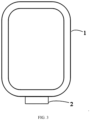
- the display device may include a display panel 1 and a controller 2, wherein the display panel 1 has the pixel driving circuit of any implementation solution in embodiment 1, and the controller 2 is configured to carry out the pixel driving method of any implementation solution in embodiment 2.
- the display device of the embodiment of the present disclosure may be an active-matrix organic light-emitting diode (AMOLED) display which has many advantages such as slim body, power saving, bright color and high picture quality and has been widely used.
- AMOLED display gradually plays a dominant role in the field of flat panel display, such as an OLED television, a mobile phone, a notebook computer.
- the description with reference to the term “some embodiments”, “exemplarily”, “in some alternative embodiments” or the like means that a specific feature, structure, material or characteristic described in combination with the embodiment(s) or example(s) are included in at least one embodiment or example of the present disclosure.
- the schematic representation of the above terms is not necessarily directed to the same embodiment or example.
- the specific features, structures, materials or characteristics described may be combined in any one or more of embodiments or examples in a suitable manner.
- a person skilled in the art may combine different embodiments or examples described herein and features of different embodiments or examples without any contradiction.
Landscapes
- Engineering & Computer Science (AREA)
- Physics & Mathematics (AREA)
- Computer Hardware Design (AREA)
- General Physics & Mathematics (AREA)
- Theoretical Computer Science (AREA)
- Control Of Indicators Other Than Cathode Ray Tubes (AREA)
- Control Of El Displays (AREA)
- Devices For Indicating Variable Information By Combining Individual Elements (AREA)
- Electroluminescent Light Sources (AREA)
Applications Claiming Priority (2)
| Application Number | Priority Date | Filing Date | Title |
|---|---|---|---|
| CN202211398611.7A CN115440163B (zh) | 2022-11-09 | 2022-11-09 | 像素驱动电路、像素驱动方法及显示装置 |
| PCT/CN2023/095261 WO2024098712A1 (fr) | 2022-11-09 | 2023-05-19 | Circuit d'attaque de pixel, procédé d'attaque de pixel et appareil d'affichage |
Publications (2)
| Publication Number | Publication Date |
|---|---|
| EP4390906A1 true EP4390906A1 (fr) | 2024-06-26 |
| EP4390906A4 EP4390906A4 (fr) | 2024-10-30 |
Family
ID=84252682
Family Applications (1)
| Application Number | Title | Priority Date | Filing Date |
|---|---|---|---|
| EP23864102.1A Pending EP4390906A4 (fr) | 2022-11-09 | 2023-05-19 | Circuit d'attaque de pixel, procédé d'attaque de pixel et appareil d'affichage |
Country Status (6)
| Country | Link |
|---|---|
| US (1) | US11842687B1 (fr) |
| EP (1) | EP4390906A4 (fr) |
| JP (1) | JP7646950B2 (fr) |
| KR (1) | KR102812675B1 (fr) |
| CN (1) | CN115440163B (fr) |
| WO (1) | WO2024098712A1 (fr) |
Families Citing this family (2)
| Publication number | Priority date | Publication date | Assignee | Title |
|---|---|---|---|---|
| CN115440163B (zh) * | 2022-11-09 | 2023-01-03 | 惠科股份有限公司 | 像素驱动电路、像素驱动方法及显示装置 |
| CN116416940B (zh) * | 2023-06-07 | 2023-08-11 | 惠科股份有限公司 | 显示驱动电路、显示驱动方法及显示面板 |
Family Cites Families (26)
| Publication number | Priority date | Publication date | Assignee | Title |
|---|---|---|---|---|
| KR101117731B1 (ko) * | 2010-01-05 | 2012-03-07 | 삼성모바일디스플레이주식회사 | 화소 회로 및 유기전계발광 표시 장치, 및 이의 구동 방법 |
| CN102842283B (zh) * | 2012-08-14 | 2014-12-10 | 京东方科技集团股份有限公司 | 一种像素电路、显示装置及其驱动方法 |
| CN103021331B (zh) * | 2012-11-30 | 2016-02-24 | 北京京东方光电科技有限公司 | 一种像素驱动电路及其驱动方法、阵列基板和显示装置 |
| CN104715723B (zh) * | 2015-03-19 | 2017-08-29 | 北京大学深圳研究生院 | 显示装置及其像素电路和驱动方法 |
| CN104933993B (zh) | 2015-07-17 | 2017-12-08 | 合肥鑫晟光电科技有限公司 | 像素驱动电路及其驱动方法、显示装置 |
| KR102524459B1 (ko) * | 2015-08-27 | 2023-04-25 | 삼성디스플레이 주식회사 | 화소 및 그의 구동방법 |
| CN106803417A (zh) * | 2017-03-02 | 2017-06-06 | 深圳市华星光电技术有限公司 | 像素补偿电路及驱动方法、显示装置 |
| CN106782286B (zh) * | 2017-03-06 | 2020-01-17 | 京东方科技集团股份有限公司 | 显示装置、显示面板和像素驱动电路 |
| CN106991968B (zh) * | 2017-05-27 | 2020-11-27 | 京东方科技集团股份有限公司 | 像素补偿电路及补偿方法、显示装置 |
| WO2019186857A1 (fr) | 2018-03-29 | 2019-10-03 | シャープ株式会社 | Dispositif d'affichage et son procédé d'attaque |
| CN108806606B (zh) * | 2018-06-15 | 2019-09-27 | 中国科学院微电子研究所 | 像素补偿电路 |
| KR102564356B1 (ko) * | 2018-12-06 | 2023-08-08 | 엘지디스플레이 주식회사 | 화소회로, 유기발광표시장치 및 그의 구동방법 |
| KR102662881B1 (ko) * | 2018-12-31 | 2024-05-03 | 엘지디스플레이 주식회사 | 광학 지문 센싱 회로를 포함한 화소 회로, 화소 회로의 구동 방법, 및 유기 발광 표시 장치 |
| CN110164378B (zh) * | 2019-05-09 | 2021-11-30 | 南华大学 | Amoled像素电路及其驱动方法 |
| CN110223639B (zh) * | 2019-06-17 | 2021-01-29 | 京东方科技集团股份有限公司 | 像素电路、像素驱动方法、显示基板和显示装置 |
| KR102733086B1 (ko) * | 2019-12-30 | 2024-11-25 | 엘지디스플레이 주식회사 | 전계 발광 표시장치 |
| CN111739470B (zh) * | 2020-07-28 | 2021-11-30 | 京东方科技集团股份有限公司 | 像素驱动电路、驱动方法及显示面板 |
| KR102880006B1 (ko) * | 2020-09-11 | 2025-11-04 | 삼성디스플레이 주식회사 | 유기 발광 표시 장치의 화소 및 유기 발광 표시 장치 |
| KR102832800B1 (ko) * | 2020-09-25 | 2025-07-11 | 삼성디스플레이 주식회사 | 표시 장치 |
| CN113223458B (zh) * | 2021-01-25 | 2023-01-31 | 重庆京东方显示技术有限公司 | 一种像素电路及其驱动方法、显示基板和显示装置 |
| CN113487996B (zh) * | 2021-07-22 | 2024-07-05 | 上海闻泰信息技术有限公司 | 像素驱动电路、显示面板及显示设备 |
| CN114093319A (zh) * | 2021-11-26 | 2022-02-25 | 长沙惠科光电有限公司 | 像素补偿电路、像素驱动方法及显示装置 |
| CN114093320A (zh) * | 2021-11-26 | 2022-02-25 | 长沙惠科光电有限公司 | 像素电路、像素驱动方法及显示装置 |
| CN114822413A (zh) * | 2022-05-10 | 2022-07-29 | 绵阳惠科光电科技有限公司 | 像素电路、像素驱动方法及显示装置 |
| CN115035854A (zh) * | 2022-06-24 | 2022-09-09 | 惠科股份有限公司 | 像素驱动电路、驱动方法和显示装置 |
| CN115440163B (zh) * | 2022-11-09 | 2023-01-03 | 惠科股份有限公司 | 像素驱动电路、像素驱动方法及显示装置 |
-
2022
- 2022-11-09 CN CN202211398611.7A patent/CN115440163B/zh active Active
-
2023
- 2023-05-19 KR KR1020247018452A patent/KR102812675B1/ko active Active
- 2023-05-19 WO PCT/CN2023/095261 patent/WO2024098712A1/fr not_active Ceased
- 2023-05-19 JP JP2024538720A patent/JP7646950B2/ja active Active
- 2023-05-19 EP EP23864102.1A patent/EP4390906A4/fr active Pending
- 2023-06-06 US US18/330,059 patent/US11842687B1/en active Active
Also Published As
| Publication number | Publication date |
|---|---|
| US11842687B1 (en) | 2023-12-12 |
| CN115440163B (zh) | 2023-01-03 |
| JP2024545473A (ja) | 2024-12-06 |
| KR20240096657A (ko) | 2024-06-26 |
| EP4390906A4 (fr) | 2024-10-30 |
| JP7646950B2 (ja) | 2025-03-17 |
| WO2024098712A1 (fr) | 2024-05-16 |
| CN115440163A (zh) | 2022-12-06 |
| KR102812675B1 (ko) | 2025-05-23 |
Similar Documents
| Publication | Publication Date | Title |
|---|---|---|
| US20220406865A1 (en) | Element substrate and light-emitting device | |
| US10410583B2 (en) | Display device, method of laying out light emitting elements, and electronic device | |
| US8345031B2 (en) | Display device, driving method for display device, and electronic apparatus | |
| US20100149153A1 (en) | Display device, display device drive method, and electronic apparatus | |
| EP3621060A1 (fr) | Procédé d'attaque de circuit de pixels | |
| US11462168B2 (en) | Pixel circuit and driving method thereof, light-emitting control circuit, display panel, and display device | |
| US20230402002A1 (en) | Pixel driving circuit, pixel driving method and display panel | |
| EP4390906A1 (fr) | Circuit d'attaque de pixel, procédé d'attaque de pixel et appareil d'affichage | |
| US12080214B2 (en) | Display panel, drive circuit and display device | |
| US8098241B2 (en) | Display device, electronic device, and method of driving display device | |
| CN114822413A (zh) | 像素电路、像素驱动方法及显示装置 | |
| US20120286275A1 (en) | Display device and electronic apparatus | |
| US11942036B2 (en) | Pixel circuit, pixel circuit driving method and display device | |
| US20250322792A1 (en) | Pixel driving circuit, display panel and display device | |
| CN120936199A (zh) | 显示面板及显示装置 |
Legal Events
| Date | Code | Title | Description |
|---|---|---|---|
| STAA | Information on the status of an ep patent application or granted ep patent |
Free format text: STATUS: UNKNOWN |
|
| STAA | Information on the status of an ep patent application or granted ep patent |
Free format text: STATUS: THE INTERNATIONAL PUBLICATION HAS BEEN MADE |
|
| PUAI | Public reference made under article 153(3) epc to a published international application that has entered the european phase |
Free format text: ORIGINAL CODE: 0009012 |
|
| STAA | Information on the status of an ep patent application or granted ep patent |
Free format text: STATUS: REQUEST FOR EXAMINATION WAS MADE |
|
| 17P | Request for examination filed |
Effective date: 20240319 |
|
| AK | Designated contracting states |
Kind code of ref document: A1 Designated state(s): AL AT BE BG CH CY CZ DE DK EE ES FI FR GB GR HR HU IE IS IT LI LT LU LV MC ME MK MT NL NO PL PT RO RS SE SI SK SM TR |
|
| RIN1 | Information on inventor provided before grant (corrected) |
Inventor name: KANG, BAOHONG Inventor name: FAN, TAO |
|
| REG | Reference to a national code |
Ref country code: DE Ref legal event code: R079 Free format text: PREVIOUS MAIN CLASS: G09G0003320000 Ipc: G09G0003323300 |
|
| A4 | Supplementary search report drawn up and despatched |
Effective date: 20240926 |
|
| RIC1 | Information provided on ipc code assigned before grant |
Ipc: G09G 3/3233 20160101AFI20240920BHEP |
|
| GRAJ | Information related to disapproval of communication of intention to grant by the applicant or resumption of examination proceedings by the epo deleted |
Free format text: ORIGINAL CODE: EPIDOSDIGR1 |
|
| GRAP | Despatch of communication of intention to grant a patent |
Free format text: ORIGINAL CODE: EPIDOSNIGR1 |
|
| GRAP | Despatch of communication of intention to grant a patent |
Free format text: ORIGINAL CODE: EPIDOSNIGR1 |
|
| STAA | Information on the status of an ep patent application or granted ep patent |
Free format text: STATUS: GRANT OF PATENT IS INTENDED |
|
| DAV | Request for validation of the european patent (deleted) | ||
| DAX | Request for extension of the european patent (deleted) | ||
| INTG | Intention to grant announced |
Effective date: 20260210 |