EP4391064B1 - Verfahren zur herstellung von mikro-leds und resultierende struktur mit mikro-leds - Google Patents
Verfahren zur herstellung von mikro-leds und resultierende struktur mit mikro-leds Download PDFInfo
- Publication number
- EP4391064B1 EP4391064B1 EP23217472.2A EP23217472A EP4391064B1 EP 4391064 B1 EP4391064 B1 EP 4391064B1 EP 23217472 A EP23217472 A EP 23217472A EP 4391064 B1 EP4391064 B1 EP 4391064B1
- Authority
- EP
- European Patent Office
- Prior art keywords
- layer
- gan layer
- gan
- porosified
- doped gan
- Prior art date
- Legal status (The legal status is an assumption and is not a legal conclusion. Google has not performed a legal analysis and makes no representation as to the accuracy of the status listed.)
- Active
Links
Images




Classifications
-
- H—ELECTRICITY
- H10—SEMICONDUCTOR DEVICES; ELECTRIC SOLID-STATE DEVICES NOT OTHERWISE PROVIDED FOR
- H10H—INORGANIC LIGHT-EMITTING SEMICONDUCTOR DEVICES HAVING POTENTIAL BARRIERS
- H10H20/00—Individual inorganic light-emitting semiconductor devices having potential barriers, e.g. light-emitting diodes [LED]
- H10H20/80—Constructional details
- H10H20/81—Bodies
- H10H20/817—Bodies characterised by the crystal structures or orientations, e.g. polycrystalline, amorphous or porous
-
- H—ELECTRICITY
- H10—SEMICONDUCTOR DEVICES; ELECTRIC SOLID-STATE DEVICES NOT OTHERWISE PROVIDED FOR
- H10H—INORGANIC LIGHT-EMITTING SEMICONDUCTOR DEVICES HAVING POTENTIAL BARRIERS
- H10H20/00—Individual inorganic light-emitting semiconductor devices having potential barriers, e.g. light-emitting diodes [LED]
- H10H20/01—Manufacture or treatment
- H10H20/011—Manufacture or treatment of bodies, e.g. forming semiconductor layers
- H10H20/013—Manufacture or treatment of bodies, e.g. forming semiconductor layers having light-emitting regions comprising only Group III-V materials
- H10H20/0133—Manufacture or treatment of bodies, e.g. forming semiconductor layers having light-emitting regions comprising only Group III-V materials with a substrate not being Group III-V materials
- H10H20/01335—Manufacture or treatment of bodies, e.g. forming semiconductor layers having light-emitting regions comprising only Group III-V materials with a substrate not being Group III-V materials the light-emitting regions comprising nitride materials
-
- H—ELECTRICITY
- H10—SEMICONDUCTOR DEVICES; ELECTRIC SOLID-STATE DEVICES NOT OTHERWISE PROVIDED FOR
- H10H—INORGANIC LIGHT-EMITTING SEMICONDUCTOR DEVICES HAVING POTENTIAL BARRIERS
- H10H20/00—Individual inorganic light-emitting semiconductor devices having potential barriers, e.g. light-emitting diodes [LED]
- H10H20/01—Manufacture or treatment
- H10H20/011—Manufacture or treatment of bodies, e.g. forming semiconductor layers
- H10H20/018—Bonding of wafers
-
- H—ELECTRICITY
- H10—SEMICONDUCTOR DEVICES; ELECTRIC SOLID-STATE DEVICES NOT OTHERWISE PROVIDED FOR
- H10H—INORGANIC LIGHT-EMITTING SEMICONDUCTOR DEVICES HAVING POTENTIAL BARRIERS
- H10H20/00—Individual inorganic light-emitting semiconductor devices having potential barriers, e.g. light-emitting diodes [LED]
- H10H20/80—Constructional details
- H10H20/81—Bodies
- H10H20/819—Bodies characterised by their shape, e.g. curved or truncated substrates
-
- H—ELECTRICITY
- H10—SEMICONDUCTOR DEVICES; ELECTRIC SOLID-STATE DEVICES NOT OTHERWISE PROVIDED FOR
- H10H—INORGANIC LIGHT-EMITTING SEMICONDUCTOR DEVICES HAVING POTENTIAL BARRIERS
- H10H20/00—Individual inorganic light-emitting semiconductor devices having potential barriers, e.g. light-emitting diodes [LED]
- H10H20/80—Constructional details
- H10H20/81—Bodies
- H10H20/822—Materials of the light-emitting regions
- H10H20/824—Materials of the light-emitting regions comprising only Group III-V materials, e.g. GaP
- H10H20/825—Materials of the light-emitting regions comprising only Group III-V materials, e.g. GaP containing nitrogen, e.g. GaN
-
- H—ELECTRICITY
- H10—SEMICONDUCTOR DEVICES; ELECTRIC SOLID-STATE DEVICES NOT OTHERWISE PROVIDED FOR
- H10H—INORGANIC LIGHT-EMITTING SEMICONDUCTOR DEVICES HAVING POTENTIAL BARRIERS
- H10H20/00—Individual inorganic light-emitting semiconductor devices having potential barriers, e.g. light-emitting diodes [LED]
- H10H20/80—Constructional details
- H10H20/83—Electrodes
- H10H20/831—Electrodes characterised by their shape
- H10H20/8312—Electrodes characterised by their shape extending at least partially through the bodies
-
- H—ELECTRICITY
- H10—SEMICONDUCTOR DEVICES; ELECTRIC SOLID-STATE DEVICES NOT OTHERWISE PROVIDED FOR
- H10H—INORGANIC LIGHT-EMITTING SEMICONDUCTOR DEVICES HAVING POTENTIAL BARRIERS
- H10H20/00—Individual inorganic light-emitting semiconductor devices having potential barriers, e.g. light-emitting diodes [LED]
- H10H20/80—Constructional details
- H10H20/83—Electrodes
- H10H20/831—Electrodes characterised by their shape
- H10H20/8314—Electrodes characterised by their shape extending at least partially onto an outer side surface of the bodies
-
- H—ELECTRICITY
- H10—SEMICONDUCTOR DEVICES; ELECTRIC SOLID-STATE DEVICES NOT OTHERWISE PROVIDED FOR
- H10H—INORGANIC LIGHT-EMITTING SEMICONDUCTOR DEVICES HAVING POTENTIAL BARRIERS
- H10H20/00—Individual inorganic light-emitting semiconductor devices having potential barriers, e.g. light-emitting diodes [LED]
- H10H20/80—Constructional details
- H10H20/83—Electrodes
- H10H20/832—Electrodes characterised by their material
- H10H20/833—Transparent materials
-
- H—ELECTRICITY
- H10—SEMICONDUCTOR DEVICES; ELECTRIC SOLID-STATE DEVICES NOT OTHERWISE PROVIDED FOR
- H10H—INORGANIC LIGHT-EMITTING SEMICONDUCTOR DEVICES HAVING POTENTIAL BARRIERS
- H10H20/00—Individual inorganic light-emitting semiconductor devices having potential barriers, e.g. light-emitting diodes [LED]
- H10H20/80—Constructional details
- H10H20/85—Packages
- H10H20/852—Encapsulations
- H10H20/854—Encapsulations characterised by their material, e.g. epoxy or silicone resins
-
- H—ELECTRICITY
- H10—SEMICONDUCTOR DEVICES; ELECTRIC SOLID-STATE DEVICES NOT OTHERWISE PROVIDED FOR
- H10H—INORGANIC LIGHT-EMITTING SEMICONDUCTOR DEVICES HAVING POTENTIAL BARRIERS
- H10H29/00—Integrated devices, or assemblies of multiple devices, comprising at least one light-emitting semiconductor element covered by group H10H20/00
- H10H29/10—Integrated devices comprising at least one light-emitting semiconductor component covered by group H10H20/00
- H10H29/14—Integrated devices comprising at least one light-emitting semiconductor component covered by group H10H20/00 comprising multiple light-emitting semiconductor components
- H10H29/142—Two-dimensional arrangements, e.g. asymmetric LED layout
-
- H—ELECTRICITY
- H10—SEMICONDUCTOR DEVICES; ELECTRIC SOLID-STATE DEVICES NOT OTHERWISE PROVIDED FOR
- H10W—GENERIC PACKAGES, INTERCONNECTIONS, CONNECTORS OR OTHER CONSTRUCTIONAL DETAILS OF DEVICES COVERED BY CLASS H10
- H10W90/00—Package configurations
-
- H—ELECTRICITY
- H10—SEMICONDUCTOR DEVICES; ELECTRIC SOLID-STATE DEVICES NOT OTHERWISE PROVIDED FOR
- H10H—INORGANIC LIGHT-EMITTING SEMICONDUCTOR DEVICES HAVING POTENTIAL BARRIERS
- H10H20/00—Individual inorganic light-emitting semiconductor devices having potential barriers, e.g. light-emitting diodes [LED]
- H10H20/01—Manufacture or treatment
- H10H20/032—Manufacture or treatment of electrodes
-
- H—ELECTRICITY
- H10—SEMICONDUCTOR DEVICES; ELECTRIC SOLID-STATE DEVICES NOT OTHERWISE PROVIDED FOR
- H10H—INORGANIC LIGHT-EMITTING SEMICONDUCTOR DEVICES HAVING POTENTIAL BARRIERS
- H10H20/00—Individual inorganic light-emitting semiconductor devices having potential barriers, e.g. light-emitting diodes [LED]
- H10H20/80—Constructional details
- H10H20/81—Bodies
- H10H20/817—Bodies characterised by the crystal structures or orientations, e.g. polycrystalline, amorphous or porous
- H10H20/818—Bodies characterised by the crystal structures or orientations, e.g. polycrystalline, amorphous or porous within the light-emitting regions
-
- H—ELECTRICITY
- H10—SEMICONDUCTOR DEVICES; ELECTRIC SOLID-STATE DEVICES NOT OTHERWISE PROVIDED FOR
- H10H—INORGANIC LIGHT-EMITTING SEMICONDUCTOR DEVICES HAVING POTENTIAL BARRIERS
- H10H20/00—Individual inorganic light-emitting semiconductor devices having potential barriers, e.g. light-emitting diodes [LED]
- H10H20/80—Constructional details
- H10H20/84—Coatings, e.g. passivation layers or antireflective coatings
Definitions
- the present invention relates to the general field of color micro-screens.
- the invention relates to a method for manufacturing micro-LEDs.
- the invention also relates to a structure thus obtained.
- the invention is particularly interesting because it makes it possible to improve the uniformity and reproducibility of emission of micro-screens based on micro-LEDs, in particular GaN-type micro-LEDs.
- the invention finds applications in numerous industrial fields, and in particular in the field of color micro-screens based on micro-LEDs.
- Color microdisplays consist of pixels made up of blue, green, and red subpixels (RGB pixels). In the following description, these subpixels will be referred to simply as pixels for the sake of brevity.
- Blue and green pixels can be made from nitride materials, and red pixels from phosphide materials. Red pixels can also be made from nitride materials, for example, by growing them on a substrate containing porous GaN.
- a GaN-based light-emitting diode (LED) microdisplay consists of a single micro LED array on a substrate containing a CMOS circuit. One LED corresponds to one pixel. Each LED is connected to the CMOS circuit.
- a GaN epitaxy and an upper anode can be pixelated directly on the growth substrate (in sapphire or Si), an electrode (cathode) can be deposited (with or without contact with the n-GaN), then metal pads added by microelectronic means to allow a transfer with interconnection of the substrate containing the pixels on the CMOS control circuit.
- the removal of the growth substrate and the thinning of the GaN allows to add electrical functions on the rear face (contact with the n-GaN if not made on the front face), as well as to limit the cross talk between pixels and to add optical functions on the light emission side (for example in the upper passivation layers).
- Another method for manufacturing micro-LEDs consists of bonding a non-pixelated GaN epitaxy and anode directly onto a silicon wafer containing the CMOS circuit.
- the bonding is a metallic bonding allowing the conduction of electric current (eutectic or direct bonding).
- this CMOS circuit and GaN epitaxy assembly is thinned in order to subsequently use traditional microelectronics processes.
- the epitaxy as well as the bonding layer are then pixelated in order to individualize the micro-LEDs of the micro-screen matrix. Each of the micro-LEDs can then be addressed by the CMOS circuit.
- An upper electrode allows contact with the n-GaN either by lateral contact with the n-GaN (for example aluminum) or by contact above the n-GaN layer with a transparent conductive layer, for example, indium tin oxide (or ITO for "indium tin oxide ").
- a transparent conductive layer for example, indium tin oxide (or ITO for "indium tin oxide ").
- ITO indium tin oxide
- An encapsulation layer is then deposited above the GaN.
- the encapsulation layer is, classically, made from SiN whose optical index is also between 1.9 and 2.1.
- the optical index of GaN is approximately 2.4.
- TTV total thickness variation
- the thickness variations can lead to a variation in the optical performances of the LED (luminance, angular emission, spectrum etc.), in particular when the anode is a mirror, and the LED thus formed is of the resonant cavity type (emissive source in a Fabry-Pérot resonator).
- Changing the GaN thickness will change the optical cavity formed between the anode, the GaN and the upper optical interface (ITO/SiN in the previous example), which changes the extraction (in the SiN in the example) and consequently the extraction in air.
- micro-lens or meta-surface devices are structured in the upper encapsulation layer in order to maximize light extraction and/or to redirect the optical flow in a specific direction
- the uniformity of the emission in this passivation layer is even more important. Indeed, the efficiency of these devices depends on the angular emission in the passivation layer.
- the uniformity of the emission in air (or the control of the extraction in air) can be improved by introducing an anti-reflection layer at the passivation layer/air interface or by depositing a very thick passivation layer (typically around ⁇ 1 ⁇ m).
- Adding anti-reflection to the encapsulation layer prevents light from returning to the stack.
- the uniformity of emission in air will only be good if the emission in the encapsulating layer is uniform.
- Emission uniformity in SiN can be achieved by broadening the LED emission spectrum (but this is not what is sought for this type of device) or by thickening the n-GaN but this also tends to decrease the EQE.
- optical interference phenomena also called optical crosstalk
- the thickness of the Bragg mirrors reaches several ⁇ m, which poses a form factor problem for microelectronics integration processes.
- the devices described are several tens of micrometers on each side.
- the epitaxial stack is particularly complex (because it contains an alternation of heavily doped and less doped layers), and induces an increase in the resistivity of the ⁇ LEDs (porous n-GaN being generally less conductive than non-porous).
- An aim of the present invention is to propose a method which overcomes the drawbacks of the prior art, and which makes it possible, in particular, to manufacture a micro-LED having a uniform and repeatable emission despite process variations.
- Steps ii) and iii) may be carried out in the order ii) and iii) or in the order iii) and ii).
- Step ii) is carried out in such a way that the optical index of the porosified GaN layer does not vary by more than 10% relative to the optical index of the second electrode and/or relative to the optical index of the encapsulation layer. Preferably, it does not vary by more than 5% and even more preferably it does not vary by more than 2% relative to the optical index of the second electrode and/or of the encapsulation layer.
- the optical index n eff of the porosified GaN layer depends on the volume concentration of pores in the layer. It will be chosen according to the materials of the transparent conductive oxide layer and/or the encapsulation layer.
- the transparent conductive oxide layer is an indium tin oxide layer and/or the encapsulation layer is made of SiN, SiO 2 or SiON.
- the encapsulation layer has an optical index close to that of ITO.
- the encapsulation layer is made of SiN.
- the invention is fundamentally distinguished from the prior art by the presence of a layer of porosified GaN under and in contact with the layer of transparent conductive oxide or by the presence of a layer of porosified GaN under and in contact with the encapsulation layer.
- the indices of the porosified layer, the TCO layer and the encapsulation layer are close, the reflections at these interfaces are minimized, making the emission in the SiN independent of the thickness variations of the porous GaN.
- the porous GaN layer has a porosity between 40% and 70% by volume to have an effective optical index close to 1.9 (i.e. close to the optical index of the upper layers) and thus minimize reflections between the porous GaN and these upper layers.
- the porous GaN layer is placed between the anode (lower electrode) and the cathode (upper electrode, here the transparent conductive oxide layer), the porosity will not be too high for this porosified layer to be able to transport electrons.
- To maintain a conductive porous layer it is possible to implement localized differential doping of the n-GaN layer in order to maintain, at the pixel scale, a non-porosified zone.
- the fine localization of the GaN/porous GaN interface makes it possible to control the thickness of the LED cavity and thus to position the reflection interface between the GaN and the porous GaN at a constructive interference position in order to maximize light extraction. It is thus possible to reduce the thickness of the micro-LEDs by the epitaxy design , by compacting the p-GaN stack, quantum wells and n-GaN to its minimum, advantageously between 250 and 500nm, in order to maximize the coupling of the optical power in the vertical mode rather than in the in-plane guided modes.
- the gains in extraction as well as in emission uniformity will be all the more important as the GaN thickness is low.
- the GaN layers are preferably grown epitaxially.
- Porosification is achieved by electrochemical anodization. Electrochemical porosification exhibits selectivity depending on the doping level. It occurs only in the most n-doped areas (10 19 at.cm -3 for example), defined in particular during epitaxy. The position of the porous areas is then finely controlled. Thus, the thickness of non-porosified GaN will be constant regardless of the thickness variations resulting from the process. The variations, introduced by the microLED manufacturing process, are transferred to the porous layer which absorbs process variations.
- the porous layer is an optical extraction layer tolerant to thickness variations.
- Pixelation can be done before or after transfer, the growth substrate must be removed, at least if it is opaque (case Si).
- the thickness of the heavily doped GaN layer is between 100nm and 500nm, preferably between 200 and 500nm.
- the GaN thickness is greater than the TTV introduced by epitaxy and by thinning processes (of the order of 200nm).
- An anti-reflective layer can be deposited on the encapsulation layer.
- the method is a micro-LED production method by monolithic bonding of the epitaxy.
- the doped GaN layer comprises doped areas and lightly doped areas, the lightly doped areas not being porosified during step ii).
- the doped GaN layer of the mesas obtained in step iii) comprises a non-porosified central part and a porosified periphery.
- injection is improved because only the periphery of the GaN layer is porosified.
- the non-porosified area in the center of the pixel can be used to reconnect.
- the method is a micro-LED production method by flipping chips or hybrid bonding.
- the method may further comprise a step of depositing dielectric on the flank of the mesas acting as a passivation layer for the defects created during the etching of the mesas as well as the deposit of an electrically and thermally conductive element, for example based on copper, in the space between the mesas, thus creating the second metal electrode (cathode) which will be in contact with the N contact deposit in ITO or using the lateral contact.
- the invention also relates to a micro-LED structure obtained according to the method described above.
- the structure comprises a substrate of interest, the substrate of interest comprising a support substrate, a first electrode, a p-doped GaN layer, GaN/InGaN quantum wells, an n-doped GaN layer, a heavily doped GaN layer, mesas being formed in the substrate of interest.
- the mesas comprising the heavily doped GaN layer porosified, the doped GaN layer, the quantum wells, the p-doped GaN layer, the bottom electrode and a part of the support substrate.
- the mesas are covered by a second electrode formed of a transparent conductive oxide layer, preferably an indium tin oxide layer, and/or by an encapsulation layer.
- the highly doped GaN layer of the mesas comprises a non-porosified central part and a porosified periphery.
- the central part is lightly doped.
- the central part is heavily doped.
- the porosified GaN layer has a thickness of between 100 and 500 nm, preferably between 300 and 500 nm.
- the invention finds particular applications in the field of monochrome micro-screens or color micro-screens, and more particularly for the manufacture of LEDs.
- it could be used in the field of photovoltaics or even water electrolysis ( "water splitting ") since, on the one hand, InGaN absorbs in the entire visible spectrum and, on the other hand, its valence and conduction bands are around the stability domain of water, a thermodynamic condition necessary for the water decomposition reaction.
- the invention may also be of interest for the manufacture of long-wavelength emitting lasers.
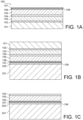
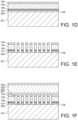
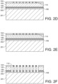
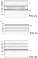
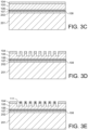
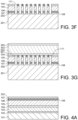
- the invention is more particularly described for a monolithic type integration by complete transfer of the layers, that is to say that the porosification step is carried out after transfer ( Figures 1A to 1F , 2A to 2G And 3A to 3G ).
- the porosification step is carried out on the growth substrate, to manufacture the LED and then to make a flip chip type assembly or hybrid bonding on a substrate comprising an integrated circuit of the ASIC type ( Application-Specific Integrated Circuit ) .
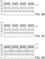
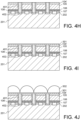
- the porosification step is carried out before transfer, which allows for relaxation during growth ( Figures 4A to 4J ).
- the process is particularly interesting for manufacturing structures comprising porosified (Al,In,Ga)N/(Al,In,Ga)N mesas having, in particular, a pitch of less than 30 ⁇ m.
- (Al,In,Ga)N we mean AIN, AlGaN, InGaN or GaN.
- porous GaN it is possible to have, for example, porous InGaN or AlGaN.
- the contact of the second electrode 301 can be made on the upper face of the layer 104' of porosified GaN, on the lateral face of the layer 104' of porosified GaN or on the lateral face of the layer 105 of doped GaN.
- the upper face of the porosified GaN layer 104' is in direct contact with the upper electrode 301 made of transparent conductive oxide or in direct contact with the encapsulation layer 302.
- direct contact it is meant that there is no intermediate layer between the aforementioned layers.
- the first stack provided in step a) comprises a base substrate 101 having, for example, a thickness ranging from 250 ⁇ m to 2 mm.
- the thickness depends on the nature of the base substrate 101 and its dimensions. For example, for a 2-inch diameter sapphire base substrate, the thickness may be 350 ⁇ m. For a 6-inch diameter sapphire support layer, the thickness may be 1.3 mm. For a 200 mm diameter silicon support layer, the thickness may be 1 mm.
- a buffer layer made of (Al,Ga)N is advantageously interposed between the substrate 101 and the layer 103 of nest-GaN. This is a buffer layer for growth.
- the GaN-nested layer 103 is an unintentionally doped (nest) layer to avoid porosification.
- Unintentionally doped GaN means a concentration lower than 5 ⁇ 10 17 at/cm 3 .
- the GaN-nested layer 103 has, for example, a thickness ranging from 500nm to 5 ⁇ m.
- its thickness is between 1 and 4 ⁇ m to absorb the stresses related to the lattice mismatch between the GaN and the underlying layers.
- the layer 104 of heavily n-doped GaN is deposited on the nested GaN layer.
- heavily doped GaN is meant a concentration greater than 6 ⁇ 10 18 at/cm 3 , preferably at least 8 ⁇ 10 18 at/cm 3 , or even greater than 10 19 at/cm 3 .
- It has a thickness between 100nm and 500 nm, preferably between 200nm and 500 nm and even more preferably between 300nm and 500 nm. This layer makes it possible to absorb the TTVs due to the micro-LED manufacturing process. This layer is porosified during step d).
- the layer 104 of heavily n-doped GaN comprises two main faces (an upper face and a lower face) parallel or substantially parallel to each other and a side face.
- the doped GaN layer 105 is formed on the heavily doped GaN layer 104.
- Doped GaN means a concentration greater than 10 18 at/cm 3 , preferably between 1 ⁇ 10 18 at/cm 3 and 5 ⁇ 10 18 at/cm 3 .
- the GaN layer has, for example, a thickness ranging from 100nm to 1 ⁇ m. It must be sufficiently electrically conductive to be able to make contact on this layer during the electrochemical anodization step. This electrically conductive layer is electrically connected to the voltage or current generator. Advantageously, it ensures the quality of the material of the upper layer. The minimum thickness varies depending on the doping rate.
- the n-doped GaN layer 105 comprises two main faces (an upper face and a lower face) parallel or substantially parallel to each other and a side face.
- n-type doping is described, but it could be p-type doping.
- the dopings could be reversed.
- 106 quantum wells are, for example, GaN/InGaN wells.
- the various GaN layers mentioned above as well as the quantum wells 106 are formed by epitaxy.
- the first stack 100 may be a more complex stack and may contain, for example, one or more of the following: an AlGaN electron blocking layer (or EBL for “Electron Blocking Layer”), a multilayer with different dopings to make porous mesas, etc.
- an AlGaN electron blocking layer or EBL for “Electron Blocking Layer”
- EBL Electrode Blocking Layer
- the first stack (p side) is transferred to a second stack comprising a support substrate 201 and a lower electrode 202 (or first electrode).
- the first electrode 108 is deposited on the first stack and then the assembly is transferred to the support substrate 201 covered by the metal layer 202.
- the support substrate 201 is preferably a substrate comprising an integrated circuit of the ASIC type, (“ Application-Specific Integrated Circuit ”) .
- the ASIC circuit may comprise electronic components (transistor(s), capacitor(s), resistors, etc.) allowing the individual control/power supply of each micro-LED according to the expected color. for the pixel.
- the electronic components are made directly in the volume (or “ bulk ”) of the substrate.
- the support substrate 201 may also be a thin-film transistor (TFT) matrix substrate, in particular to obtain larger direct-view screens.
- TFT thin-film transistor
- the substrate 201 is preferably a silicon wafer.
- the lower electrode 202 (or first electrode) covers the support substrate. It could also be made of ITO.
- the lower electrode 202 is, for example, made of aluminum or silver. It can, for example, have a thickness between 40 and 200 nm.
- the base substrate 101, the buffer layer 102 if applicable, and the GaN nest layer 103 are removed.
- the base substrate 101 is removed by laser (also called a lift -off technique) .
- the buffer layer 102 and the nest-GaN layer 103 may be removed by thinning.
- the thinning may terminate at the nest layer 103/heavily doped GaN layer 104 interface.
- the thinning terminates in the heavily doped GaN layer 104.
- step d the heavily doped GaN layer 104 is partially or completely porosified.
- step d the structure and a counter electrode (CE) are electrically connected to a voltage or current generator.
- the structure acts as a working electrode (WE).
- WE working electrode
- it will be called a voltage generator, but it could be a current generator to apply a current between the device and the counter electrode.
- the contact is made on an electrically conductive layer of the structure, preferably on the 105 layer of doped GaN.
- the counter electrode is made of an electrically conductive material, such as a metal such as platinum.
- the electrodes are immersed in an electrolyte, also called an electrolytic bath or electrolytic solution.
- the electrolyte can be acidic or basic.
- the electrolyte is, for example, oxalic acid. It can also be KOH, HF, HNO 3 , NaNO 3 or H 2 SO 4 or a mixture thereof.
- the applied voltage can be between 1 and 30V for example. Preferably, it is between 5 and 18V (for example between 5 and 15V), and even more preferably between 6 and 12V, for example between 8 and 10V.
- the voltage is chosen according to the doping rates of the different layers and the target porosity rate. It is applied, for example, for a period ranging from a few seconds to several hours. Porosification is complete when there is no longer any current at the imposed potential. At that moment, the entire doped structure is porosified and the electrochemical reaction stops.
- the electrochemical anodizing step can be carried out under ultraviolet (UV) light.
- UV ultraviolet
- the porosity rate of the porosified GaN layer 104 is at least 10%. It preferably ranges from 10% to 80%, and even more preferably from 30% to 70%.
- the largest dimension (height) of pores can vary from a few nanometers to a few micrometers.
- the smallest dimension (diameter) can vary from a few nanometers to a hundred nanometers, particularly from 30 to 70 nm.
- the porosification obtained depends on the doping of the layer and the process parameters (applied voltage, duration, nature and concentration of the electrolyte, chemical post-treatment or annealing).
- the anodization of the GaN layer 104 may be total. According to embodiment variants described in more detail below, the anodization may be partial. Otherwise, one or more areas 110 of the heavily doped GaN layer are not porosified during step d). Each non-porosified area goes from the first main face to the second main face to form an electrical conduction path through the GaN layer.
- the electrical conduction path may have the shape of a channel or a tube for example.
- step e the mesas are formed.
- the structuring of the stack is, for example, carried out by photolithography.
- Mesas also called elevations, are relief elements. They are obtained, for example, by engraving a continuous layer or several continuous layers superimposed, so as to leave only a certain number of "reliefs" of this layer or these layers remaining. layers.
- the engraving is generally plasma engraving (or dry engraving).
- the reliefs allow pixels to be defined.
- the sides of the mesas are perpendicular to this stack of layers.
- the surface of the mesas can be, for example, circular, hexagonal, square or rectangular.
- the largest dimension of the surface of the mesas ranges from 500nm to 500 ⁇ m, preferably from 1 to 10 ⁇ m and even more preferably from 3 to 5 ⁇ m.
- the largest dimension of a circular surface is the diameter.
- the thickness (or depth) of the mesas corresponds to the dimension of the mesa perpendicular to the underlying stack.
- the depth of the mesas ranges from 0.5 to 1 ⁇ m, preferably from 0.3 to 2 ⁇ m.
- the spacing between two consecutive mesas ranges from 50nm to 20 ⁇ m.
- a second electrode 301 is deposited on the porosified layer 104' (i.e. on the upper face of the porosified layer 104').
- the second electrode is a layer of transparent conductive oxide. It may be a layer of indium-tin oxide (or ITO for " indium tin oxide "), alumina-doped zinc oxide (or AZO for " aluminium-doped zinc oxide ”) , Gallium Zinc oxide (GZO) or SnO 2 . This layer covers the mesas.
- the layer of transparent conductive oxide acts as an upper electrode or cathode.
- step f it is possible to implement a step g) to deposit an encapsulation layer 302 on the transparent conductive oxide layer 301.
- the encapsulation layer 302 is, for example, a layer of SiN, SiO 2 or SiON. It could also be a multi-layer.
- Structuring of the encapsulation layer 302 by micro-lenses can also be achieved.
- an anti-reflector 303 i.e. an anti-reflection layer
- the core of the heavily doped GaN layer of the pixels is not porosified.
- the core represents, for example, from 5% to 25% of the volume of the layer.
- the local reduction of the doping rate of the heavily doped GaN layer 104 is achieved, for example, by implanting helium or hydrogen.
- the ion implantation step makes it possible to reduce the conductivity and deactivate the dopants initially present.
- the characteristics of the different layers, of the different elements described for this embodiment variant where the porosification step is implemented before the transfer step may be identical to the characteristics of the different layers, of the different elements described for the embodiment variant where the porosification step is implemented after the transfer step.
- the 104' GaN layer of the mesas can be fully porosified or partially porosified.
- the GaN layer 104' of the mesas comprises a non-porosified central part 110 and a porosified periphery.
- the central part can be lightly doped or heavily doped.
- the uniformity of the emission in the encapsulation is found in the air thanks either to a structuring which breaks the cavity effect, or by the addition of an anti-reflection layer which allows the light emitted in the encapsulation layer, in particular in SiN, to pass directly into the air without interacting again with the stack of the structure.
- Example 1 Comparative example with an LED structure covered with ITO and SiN :
- the LED stack studied successively comprises ( Figure 5A ): a layer of aluminum 202, a p-doped layer 107, quantum wells 106, a layer 105 of n-doped GaN with an optical index of 2.4, a layer of transparent conductive oxide 301 in ITO with an optical index of 1.91 and an encapsulation layer 302 in SiN with an optical index of 1.95.
- Example 2 illustrative example with an LED structure covered with ITO and SiN:
- the LED stack studied successively comprises ( Figure 6A ): a layer of aluminum 202, a p-doped layer 107, quantum wells 106, a layer 105 of n-doped GaN with an optical index of 2.4, a layer 104' of porous GaN with an optical index of 1.9, a layer of transparent conductive oxide 301 in ITO with an optical index of 1.91 and an encapsulation layer 302 in SiN with an optical index of 1.95.
- a layer of porous GaN has been added. The thickness of non-porosified GaN is chosen so as to be at a maximum extraction.
- Example 3 Comparative example with an LED structure covered with ITO, SiN and SiO 2 :
- the LED stack studied successively comprises ( Figure 7A ): an aluminum layer 202, a p-doped layer 107, quantum wells 106, an n-doped GaN layer 105 with an optical index of 2.4, a transparent conductive oxide layer 301 in ITO with an optical index of 1.91, an encapsulation layer 302 in SiN with an optical index of 1.95, an anti-reflection layer 303 in SiO 2 .
- Example 4 Illustrative example with an LED structure covered with ITO, SiN and SiO 2 :
- the LED stack studied successively comprises ( Figure 8A ): a layer of aluminum 202, a p-doped layer 107, quantum wells 106, a layer 105 of n-doped GaN with an optical index of 2.4, a layer 104' of porous GaN with an optical index of 1.9, a layer of transparent conductive oxide 301 in ITO with an optical index of 1.91, an encapsulation layer 302 in SiN with an optical index of 1.95, an anti-reflection layer 303 in SiO 2 .
- the thickness of non-porous GaN is chosen to be at maximum extraction.
- the thinner the GaN thicknesses the higher the EQEs and the greater the oscillations as a function of GaN thickness. It is likely that the oscillation effects will be stronger as the angular space is reduced, for example if the emission considered is between 0 and 18.5° in the axis perpendicular to the plane of the structure.
Landscapes
- Led Devices (AREA)
Claims (12)
- Verfahren zur Herstellung von Mikro-LEDs, das mindestens folgende Schritte umfasst:i) Bereitstellen eines Stapels, der mindestens eine n-dotierte GaN-Schicht (104), eine n-dotierte GaN-Schicht (105), Quanten-Wells (106) und eine p-dotierte GaN-Schicht (107) und eine erste Elektrode (108) umfasst,ii) Porosifizieren der stark n-dotierten GaN-Schicht (104), wodurch eine porosifizierte GaN-Schicht (104') erhalten wird,iii) Bilden von Mesas im Stapel,iv) Bedecken der porosifizierten GaN-Schicht (104') mit einer zweiten Elektrode (301), die aus einer Schicht aus leitfähigem, transparentem Oxid gebildet ist, wobei die zweite Elektrode (301) in direktem Kontakt mit der porosifizierten GaN-Schicht (104') steht, anschließend, Bedecken, vorzugsweise, der zweiten Elektrode (301) mit einer Kapselschicht (302),oderAblegen einer zweiten Elektrode (301) auf eine Seitenfläche der porosifizierten GaN-Schicht (104') oder auf eine Seitenfläche der n-dotierten GaN-Schicht (105) und die porosifizierten GaN-Schicht (104') mit einer Kapselschicht (302) bedecken, wobei die Kapselschicht (302) in direktem Kontakt mit der porosifizierten GaN-Schicht (104') steht,wobei die Schritte ii) und iii) in der Reihenfolge ii) und iii) oder in der Reihenfolge iii) und ii) durchgeführt werden können,wobei Schritt ii) so ausgeführt ist, dass der optische Index der porosifizierten GaN-Schicht (104') nicht um mehr als 10 % im Verhältnis zum optischen Index der zweiten Elektrode (301) und/oder im Verhältnis zum optischen Index der Kapselschicht (302) variiert.
- Verfahren nach Anspruch 1, wobei die leitfähige transparente Oxidschicht eine Zinn-Indiumoxidschicht ist und/oder die Kapselschicht (302) aus SiN, SiO2 oder SiON besteht.
- Verfahren nach einem der Ansprüche 1 bis 2, wobei die Volumenkonzentration von Poren in der porosifizierten GaN-Schicht (104') nach folgender Formel bestimmt wird:

- Verfahren nach einem der Ansprüche 1 bis 3, dadurch gekennzeichnet, dass der Schritt i) nach folgenden aufeinanderfolgenden Schritten a) bis c) durchgeführt wird:a) Bereitstellen eines Anfangsstapels (100) umfassend eine Trägerschicht (101), gegebenenfalls eine Pufferschicht aus (Al,Ga)N (102), eine nicht absichtlich dotierte GaN-Schicht (103), die stark n-dotierte GaN-Schicht (104), die n-dotierte GaN-Schicht (105), die Quanten-Wells (106), die p-dotierte GaN-Schicht (107) und die erste Elektrode (108),b) Übertragen des ursprünglichen Stapels (100) auf ein Trägersubstrat (201), das mit einer Metallschicht (202) bedeckt ist,c) Entfernen der Trägerschicht (101), gegebenenfalls der (Al,Ga)N-Pufferschicht (102), der nicht absichtlich dotierten GaN-Schicht (103), beispielsweise durch Ausdünnen, wodurch ein zu untersuchendes Substrat erhalten wird, das das Trägersubstrat (201), die erste Elektrode (108), die p-dotierte GaN-Schicht (107), die GaN/InGaN-Quanten-Wells (106), die n-dotierte GaN-Schicht (105) und die stark n-dotierte GaN-Schicht (104) umfasst.
- Verfahren nach Anspruch 4, wobei das Verfahren vor Schritt ii) einen Schritt umfasst, bei dem die Dotierungsrate der stark n-dotierten GaN-Schicht (104) lokal verringert wird, beispielsweise durch Implantation von Helium- oder Wasserstoffionen, so dass ein erster Teil der stark n-dotierten GaN-Schicht (104) eine erste Leitfähigkeit und ein zweiter Teil (110) eine zweite Leitfähigkeit aufweist, wobei die erste elektrische Leitfähigkeit um mindestens einen Faktor zehn höher ist als die zweite elektrische Leitfähigkeit, wodurch:- der zweite Teil (110) in Schritt ii) nicht porosifiziert ist,- die porosifizierte GaN-Schicht (104') der in Schritt iii) erhaltenen Mesas einen nicht porosifizierten Teil (110) und einen porosifizierten Teil umfasst, wobei der nicht porosifizierte Teil (110) vorzugsweise in der Mitte des porosifizierten Teils liegt.
- Verfahren nach Anspruch 4, wobei:- das Verfahren einen zusätzlichen Schritt zwischen Schritt i) und Schritt ii) umfasst, bei dem die stark n-dotierte GaN-Schicht (104) und ein Teil der n-dotierten GaN-Schicht (105) geätzt werden, um eine Mesas-Vorstruktur zu bilden,- bei Schritt ii) ein Mittelteil (111) der stark n-dotierten GaN-Schicht (104) nicht porosifiziert wird, indem beispielsweise der Porosifizierungsschritt vor der vollständigen Porosifizierung der stark dotierten GaN-Schicht (104) gestoppt wird, wodurch die GaN-Schicht (104') der in Schritt iii) erhaltenen Mesas den nicht porosifizierten Mittelteil (111) und einen porosifizierten Umfang umfasst,- Schritt iii) durch Ätzen des anderen Teils der n-dotierten GaN-Schicht (105), der Quanten-Wells (106), der p-dotierten GaN-Schicht (107), der ersten Elektrode (108) und eines Teils des Trägersubstrats (201) erfolgt.
- Verfahren nach einem der Ansprüche 1 bis 3, wobei das Verfahren folgende aufeinanderfolgende Schritte umfasst:i) Bereitstellen eines Stapels, der eine Trägerschicht (101), eine nicht absichtlich dotierte GaN-Schicht (103), die stark n-dotierte GaN-Schicht (104), die n-dotierte GaN-Schicht (105), die Quanten-Wells (106) und die p-dotierte GaN-Schicht (107) und die erste Elektrode (108) umfasst,iii) Bilden von Mesas im Stapel, durch Ätzen der ersten Elektrode (108), der p-dotierten GaN-Schicht (107), der Quanten-Wells (106), der n-dotierten GaN-Schicht (105), der stark n-dotierten GaN-Schicht (104) und eines Teils der nicht absichtlich dotierten GaN-Schicht (103),- Durchführen des Schritts ii), wobei eine porosifizierte GaN-Schicht (104') erhalten wird,- Übertragen des erhaltenen Stapels auf ein Trägersubstrat (201), das mit einer Metallschicht (202) bedeckt ist,- Entfernen der Trägerschicht (101), der nicht absichtlich dotierten GaN-Schicht (103), beispielsweise durch Ausdünnen, wodurch ein Substrat von Interesse erhalten wird, das das Trägersubstrat (201), die erste Elektrode (108), die p-dotierte GaN-Schicht (107), die GaN/InGaN-Quanten-Wells (106), die n-dotierte GaN-Schicht (105) und die stark n-dotierte GaN-Schicht (104) umfasst,- Durchführen von Schritt iv).
- Struktur von Mikro-LEDs, umfassend einen Stapel, wobei der Stapel mindestens eine stark n-dotierte, porosifizierte GaN-Schicht (104'), eine n-dotierte GaN-Schicht (105), Quanten-Wells (106) und eine p-dotierte GaN-Schicht (107) umfasst, wobei eine erste Elektrode (108) ist, wobei im Stapel Mesas gebildet sind,wobei die porosifizierte GaN-Schicht (104') bedeckt ist und in direktem Kontakt mit einer zweiten Elektrode (301) steht, die aus einer Schicht aus leitfähigem, transparentem Oxid gebildet ist, wobei die zweite Elektrode (301) vorzugsweise von einer Kapselschicht (302) bedeckt ist,
oderwobei eine zweite Elektrode (301) an einer Seitenfläche der porosifizierten GaN-Schicht (104') oder an einer Seitenfläche der n-dotierten GaN-Schicht (105) angeordnet ist, wobei die porosifizierte GaN-Schicht (104') bedeckt ist und in direktem Kontakt mit einer Kapselschicht (302) steht,wobei, in jedem Fall, der optische Index der porosifizierten GaN-Schicht (104') nicht mehr als 10 % im Verhältnis zum optischen Index der zweiten Elektrode (301) und/oder im Verhältnis zum optischen Index der Kapselschicht (302) variiert. - Struktur nach Anspruch 8, wobei die porosifizierte GaN-Schicht (104') der Mesas einen nicht porosifizierten Mittelteil (110, 111) und einen porosifizierten Umfang umfasst.
- Struktur nach Anspruch 9, wobei der Mittelteil (110) schwach dotiert ist.
- Struktur nach Anspruch 9, wobei der Mittelteil (111) stark dotiert ist.
- Struktur nach einem der Ansprüche 8 bis 11, wobei die porosifizierte GaN-Schicht (104') eine Dicke zwischen 100 und 500 nm, vorzugsweise zwischen 300 und 500 nm aufweist.
Applications Claiming Priority (1)
| Application Number | Priority Date | Filing Date | Title |
|---|---|---|---|
| FR2214156A FR3144412B1 (fr) | 2022-12-21 | 2022-12-21 | PROCEDE DE FABRICATION DE MICRO-LEDs |
Publications (2)
| Publication Number | Publication Date |
|---|---|
| EP4391064A1 EP4391064A1 (de) | 2024-06-26 |
| EP4391064B1 true EP4391064B1 (de) | 2025-06-11 |
Family
ID=86332210
Family Applications (1)
| Application Number | Title | Priority Date | Filing Date |
|---|---|---|---|
| EP23217472.2A Active EP4391064B1 (de) | 2022-12-21 | 2023-12-18 | Verfahren zur herstellung von mikro-leds und resultierende struktur mit mikro-leds |
Country Status (4)
| Country | Link |
|---|---|
| US (1) | US20240213409A1 (de) |
| EP (1) | EP4391064B1 (de) |
| CN (1) | CN118231542A (de) |
| FR (1) | FR3144412B1 (de) |
Family Cites Families (5)
| Publication number | Priority date | Publication date | Assignee | Title |
|---|---|---|---|---|
| US11095096B2 (en) * | 2014-04-16 | 2021-08-17 | Yale University | Method for a GaN vertical microcavity surface emitting laser (VCSEL) |
| US20200251460A1 (en) * | 2017-08-25 | 2020-08-06 | Sharp Kabushiki Kaisha | Micro-led element, image display element, and production method |
| GB2592017B (en) * | 2020-02-11 | 2022-08-03 | Plessey Semiconductors Ltd | Multicolour light emitting structure |
| GB2599065B (en) * | 2020-05-22 | 2023-05-10 | Plessey Semiconductors Ltd | Light emitting device array |
| GB2598753B (en) * | 2020-09-10 | 2023-06-14 | Plessey Semiconductors Ltd | Selective optical filter for RGB LED |
-
2022
- 2022-12-21 FR FR2214156A patent/FR3144412B1/fr active Active
-
2023
- 2023-12-15 US US18/541,109 patent/US20240213409A1/en active Pending
- 2023-12-18 EP EP23217472.2A patent/EP4391064B1/de active Active
- 2023-12-20 CN CN202311758429.2A patent/CN118231542A/zh active Pending
Also Published As
| Publication number | Publication date |
|---|---|
| US20240213409A1 (en) | 2024-06-27 |
| CN118231542A (zh) | 2024-06-21 |
| FR3144412B1 (fr) | 2024-12-13 |
| EP4391064A1 (de) | 2024-06-26 |
| FR3144412A1 (fr) | 2024-06-28 |
Similar Documents
| Publication | Publication Date | Title |
|---|---|---|
| EP3840065B1 (de) | Verfahren zur herstellung einer entspannten gan/ingan-struktur und daraus resultierende struktur | |
| EP3840016A1 (de) | Verfahren zur herstellung eines substrats, das eine entspannte ingan-schicht umfasst | |
| EP3455882B1 (de) | Verfahren zur herstellung einer optoelektronischen vorrichtung mit mehreren galliumnitriddioden | |
| EP4356428A1 (de) | Verfahren zur herstellung einer nativen emissionsmatrix | |
| EP4105999B1 (de) | Verfahren zur herstellung einer nativen emissionsmatrix | |
| EP3891813A1 (de) | Mehrfarbige elektrolumineszierende anzeigevorrichtung und verfahren zur herstellung einer solchen vorrichtung | |
| EP3929634A1 (de) | Lichtemittierende vorrichtung, pixel mit einer vielzahl solcher vorrichtungen, pixelmatrix und entsprechende herstellungsverfahren | |
| EP4391064B1 (de) | Verfahren zur herstellung von mikro-leds und resultierende struktur mit mikro-leds | |
| EP4379800B1 (de) | Verfahren zur herstellung eines wachstumssubstrats mit unterschiedlichen elektrochemische porosifikationsebenen mit mesas mit unterschiedlichen porenbildungsgraden | |
| FR3118306A1 (fr) | Procédé de réalisation d’un dispositif optoélectronique comportant des LED à base de nitrure | |
| EP4394879A2 (de) | Verfahren zur porosifizierung einer (al,in,ga)n schicht | |
| EP4102579A1 (de) | Verfahren zur herstellung eines substrats mit einer relaxierten inganschicht und so erhaltenes substrat für die wiederaufnahme des wachstums einer led-struktur | |
| WO2024120963A1 (fr) | Procede de fabrication d'un dispositif optoelectronique comprenant une led et une photodiode | |
| WO2022175184A1 (fr) | Dispositif optoélectronique et son procédé de fabrication | |
| EP4383338B1 (de) | Verfahren zur herstellung einer optoelektronischen vorrichtung mit einer led und einer photodiode | |
| EP4639638A1 (de) | Verfahren zur herstellung einer mesastruktur zur herstellung eines kontaktes | |
| EP4679983A1 (de) | Verfahren zur herstellung einer photonischen vorrichtung und entsprechende photonische vorrichtung | |
| EP4521891A1 (de) | Verfahren zur porenbildung von mesa (al,in,ga)n/(al,in,ga)n | |
| EP4672925A1 (de) | Verfahren zur porenbildung von mesas | |
| FR3143850A1 (fr) | Procédé de réalisation d’un dispositif électronique |
Legal Events
| Date | Code | Title | Description |
|---|---|---|---|
| PUAI | Public reference made under article 153(3) epc to a published international application that has entered the european phase |
Free format text: ORIGINAL CODE: 0009012 |
|
| STAA | Information on the status of an ep patent application or granted ep patent |
Free format text: STATUS: REQUEST FOR EXAMINATION WAS MADE |
|
| 17P | Request for examination filed |
Effective date: 20231218 |
|
| AK | Designated contracting states |
Kind code of ref document: A1 Designated state(s): AL AT BE BG CH CY CZ DE DK EE ES FI FR GB GR HR HU IE IS IT LI LT LU LV MC ME MK MT NL NO PL PT RO RS SE SI SK SM TR |
|
| RAP3 | Party data changed (applicant data changed or rights of an application transferred) |
Owner name: COMMISSARIAT A L'ENERGIE ATOMIQUE ET AUX ENERGIESALTERNATIVES |
|
| REG | Reference to a national code |
Ref country code: DE Ref legal event code: R079 Free format text: PREVIOUS MAIN CLASS: H01L0027150000 Ipc: H10H0020010000 Ref document number: 602023003971 Country of ref document: DE |
|
| GRAP | Despatch of communication of intention to grant a patent |
Free format text: ORIGINAL CODE: EPIDOSNIGR1 |
|
| STAA | Information on the status of an ep patent application or granted ep patent |
Free format text: STATUS: GRANT OF PATENT IS INTENDED |
|
| RIC1 | Information provided on ipc code assigned before grant |
Ipc: H10H 20/84 20250101ALN20250307BHEP Ipc: H10H 20/818 20250101ALN20250307BHEP Ipc: H10H 20/854 20250101ALI20250307BHEP Ipc: H10H 20/833 20250101ALI20250307BHEP Ipc: H10H 20/831 20250101ALI20250307BHEP Ipc: H10H 20/825 20250101ALI20250307BHEP Ipc: H10H 20/817 20250101ALI20250307BHEP Ipc: H10H 29/14 20250101ALI20250307BHEP Ipc: H10H 20/01 20250101AFI20250307BHEP |
|
| INTG | Intention to grant announced |
Effective date: 20250321 |
|
| RIN1 | Information on inventor provided before grant (corrected) |
Inventor name: AVENTURIER, BERNARD Inventor name: LEVY, FRANCOIS Inventor name: SIMON, JULIA Inventor name: PERNEL, CAROLE Inventor name: MICHIT, NICOLAS Inventor name: DE MARTINO, PAOLO Inventor name: ALTAZIN, STEPHANE |
|
| GRAS | Grant fee paid |
Free format text: ORIGINAL CODE: EPIDOSNIGR3 |
|
| GRAA | (expected) grant |
Free format text: ORIGINAL CODE: 0009210 |
|
| STAA | Information on the status of an ep patent application or granted ep patent |
Free format text: STATUS: THE PATENT HAS BEEN GRANTED |
|
| AK | Designated contracting states |
Kind code of ref document: B1 Designated state(s): AL AT BE BG CH CY CZ DE DK EE ES FI FR GB GR HR HU IE IS IT LI LT LU LV MC ME MK MT NL NO PL PT RO RS SE SI SK SM TR |
|
| REG | Reference to a national code |
Ref country code: GB Ref legal event code: FG4D Free format text: NOT ENGLISH |
|
| REG | Reference to a national code |
Ref country code: CH Ref legal event code: EP |
|
| REG | Reference to a national code |
Ref country code: DE Ref legal event code: R096 Ref document number: 602023003971 Country of ref document: DE |
|
| REG | Reference to a national code |
Ref country code: IE Ref legal event code: FG4D Free format text: LANGUAGE OF EP DOCUMENT: FRENCH |
|
| PG25 | Lapsed in a contracting state [announced via postgrant information from national office to epo] |
Ref country code: ES Free format text: LAPSE BECAUSE OF FAILURE TO SUBMIT A TRANSLATION OF THE DESCRIPTION OR TO PAY THE FEE WITHIN THE PRESCRIBED TIME-LIMIT Effective date: 20250611 Ref country code: FI Free format text: LAPSE BECAUSE OF FAILURE TO SUBMIT A TRANSLATION OF THE DESCRIPTION OR TO PAY THE FEE WITHIN THE PRESCRIBED TIME-LIMIT Effective date: 20250611 |
|
| REG | Reference to a national code |
Ref country code: LT Ref legal event code: MG9D |
|
| PG25 | Lapsed in a contracting state [announced via postgrant information from national office to epo] |
Ref country code: GR Free format text: LAPSE BECAUSE OF FAILURE TO SUBMIT A TRANSLATION OF THE DESCRIPTION OR TO PAY THE FEE WITHIN THE PRESCRIBED TIME-LIMIT Effective date: 20250912 Ref country code: NO Free format text: LAPSE BECAUSE OF FAILURE TO SUBMIT A TRANSLATION OF THE DESCRIPTION OR TO PAY THE FEE WITHIN THE PRESCRIBED TIME-LIMIT Effective date: 20250911 |
|
| REG | Reference to a national code |
Ref country code: NL Ref legal event code: MP Effective date: 20250611 |
|
| PG25 | Lapsed in a contracting state [announced via postgrant information from national office to epo] |
Ref country code: BG Free format text: LAPSE BECAUSE OF FAILURE TO SUBMIT A TRANSLATION OF THE DESCRIPTION OR TO PAY THE FEE WITHIN THE PRESCRIBED TIME-LIMIT Effective date: 20250611 |
|
| PG25 | Lapsed in a contracting state [announced via postgrant information from national office to epo] |
Ref country code: HR Free format text: LAPSE BECAUSE OF FAILURE TO SUBMIT A TRANSLATION OF THE DESCRIPTION OR TO PAY THE FEE WITHIN THE PRESCRIBED TIME-LIMIT Effective date: 20250611 |
|
| PG25 | Lapsed in a contracting state [announced via postgrant information from national office to epo] |
Ref country code: RS Free format text: LAPSE BECAUSE OF FAILURE TO SUBMIT A TRANSLATION OF THE DESCRIPTION OR TO PAY THE FEE WITHIN THE PRESCRIBED TIME-LIMIT Effective date: 20250911 |
|
| PG25 | Lapsed in a contracting state [announced via postgrant information from national office to epo] |
Ref country code: LV Free format text: LAPSE BECAUSE OF FAILURE TO SUBMIT A TRANSLATION OF THE DESCRIPTION OR TO PAY THE FEE WITHIN THE PRESCRIBED TIME-LIMIT Effective date: 20250611 |
|
| PG25 | Lapsed in a contracting state [announced via postgrant information from national office to epo] |
Ref country code: NL Free format text: LAPSE BECAUSE OF FAILURE TO SUBMIT A TRANSLATION OF THE DESCRIPTION OR TO PAY THE FEE WITHIN THE PRESCRIBED TIME-LIMIT Effective date: 20250611 |
|
| PG25 | Lapsed in a contracting state [announced via postgrant information from national office to epo] |
Ref country code: PT Free format text: LAPSE BECAUSE OF FAILURE TO SUBMIT A TRANSLATION OF THE DESCRIPTION OR TO PAY THE FEE WITHIN THE PRESCRIBED TIME-LIMIT Effective date: 20251013 |
|
| REG | Reference to a national code |
Ref country code: AT Ref legal event code: MK05 Ref document number: 1803301 Country of ref document: AT Kind code of ref document: T Effective date: 20250611 |
|
| PG25 | Lapsed in a contracting state [announced via postgrant information from national office to epo] |
Ref country code: IS Free format text: LAPSE BECAUSE OF FAILURE TO SUBMIT A TRANSLATION OF THE DESCRIPTION OR TO PAY THE FEE WITHIN THE PRESCRIBED TIME-LIMIT Effective date: 20251011 |
|
| PG25 | Lapsed in a contracting state [announced via postgrant information from national office to epo] |
Ref country code: SM Free format text: LAPSE BECAUSE OF FAILURE TO SUBMIT A TRANSLATION OF THE DESCRIPTION OR TO PAY THE FEE WITHIN THE PRESCRIBED TIME-LIMIT Effective date: 20250611 Ref country code: AT Free format text: LAPSE BECAUSE OF FAILURE TO SUBMIT A TRANSLATION OF THE DESCRIPTION OR TO PAY THE FEE WITHIN THE PRESCRIBED TIME-LIMIT Effective date: 20250611 |
|
| PGFP | Annual fee paid to national office [announced via postgrant information from national office to epo] |
Ref country code: FR Payment date: 20251222 Year of fee payment: 3 |
|
| PG25 | Lapsed in a contracting state [announced via postgrant information from national office to epo] |
Ref country code: CZ Free format text: LAPSE BECAUSE OF FAILURE TO SUBMIT A TRANSLATION OF THE DESCRIPTION OR TO PAY THE FEE WITHIN THE PRESCRIBED TIME-LIMIT Effective date: 20250611 |
|
| PG25 | Lapsed in a contracting state [announced via postgrant information from national office to epo] |
Ref country code: PL Free format text: LAPSE BECAUSE OF FAILURE TO SUBMIT A TRANSLATION OF THE DESCRIPTION OR TO PAY THE FEE WITHIN THE PRESCRIBED TIME-LIMIT Effective date: 20250611 |
|
| PG25 | Lapsed in a contracting state [announced via postgrant information from national office to epo] |
Ref country code: EE Free format text: LAPSE BECAUSE OF FAILURE TO SUBMIT A TRANSLATION OF THE DESCRIPTION OR TO PAY THE FEE WITHIN THE PRESCRIBED TIME-LIMIT Effective date: 20250611 |
|
| PG25 | Lapsed in a contracting state [announced via postgrant information from national office to epo] |
Ref country code: SK Free format text: LAPSE BECAUSE OF FAILURE TO SUBMIT A TRANSLATION OF THE DESCRIPTION OR TO PAY THE FEE WITHIN THE PRESCRIBED TIME-LIMIT Effective date: 20250611 |
|
| PG25 | Lapsed in a contracting state [announced via postgrant information from national office to epo] |
Ref country code: RO Free format text: LAPSE BECAUSE OF FAILURE TO SUBMIT A TRANSLATION OF THE DESCRIPTION OR TO PAY THE FEE WITHIN THE PRESCRIBED TIME-LIMIT Effective date: 20250611 |
|
| REG | Reference to a national code |
Ref country code: DE Ref legal event code: R097 Ref document number: 602023003971 Country of ref document: DE |
|
| PG25 | Lapsed in a contracting state [announced via postgrant information from national office to epo] |
Ref country code: DK Free format text: LAPSE BECAUSE OF FAILURE TO SUBMIT A TRANSLATION OF THE DESCRIPTION OR TO PAY THE FEE WITHIN THE PRESCRIBED TIME-LIMIT Effective date: 20250611 |
|
| PGFP | Annual fee paid to national office [announced via postgrant information from national office to epo] |
Ref country code: DE Payment date: 20251222 Year of fee payment: 3 |
|
| PG25 | Lapsed in a contracting state [announced via postgrant information from national office to epo] |
Ref country code: IT Free format text: LAPSE BECAUSE OF FAILURE TO SUBMIT A TRANSLATION OF THE DESCRIPTION OR TO PAY THE FEE WITHIN THE PRESCRIBED TIME-LIMIT Effective date: 20250611 |
|
| PLBE | No opposition filed within time limit |
Free format text: ORIGINAL CODE: 0009261 |
|
| STAA | Information on the status of an ep patent application or granted ep patent |
Free format text: STATUS: NO OPPOSITION FILED WITHIN TIME LIMIT |
|
| REG | Reference to a national code |
Ref country code: CH Ref legal event code: L10 Free format text: ST27 STATUS EVENT CODE: U-0-0-L10-L00 (AS PROVIDED BY THE NATIONAL OFFICE) Effective date: 20260423 |