EP4394879A2 - Verfahren zur porosifizierung einer (al,in,ga)n schicht - Google Patents
Verfahren zur porosifizierung einer (al,in,ga)n schicht Download PDFInfo
- Publication number
- EP4394879A2 EP4394879A2 EP24174598.3A EP24174598A EP4394879A2 EP 4394879 A2 EP4394879 A2 EP 4394879A2 EP 24174598 A EP24174598 A EP 24174598A EP 4394879 A2 EP4394879 A2 EP 4394879A2
- Authority
- EP
- European Patent Office
- Prior art keywords
- layer
- gan
- doped
- mesas
- heavily doped
- Prior art date
- Legal status (The legal status is an assumption and is not a legal conclusion. Google has not performed a legal analysis and makes no representation as to the accuracy of the status listed.)
- Pending
Links
Images


Classifications
-
- H—ELECTRICITY
- H10—SEMICONDUCTOR DEVICES; ELECTRIC SOLID-STATE DEVICES NOT OTHERWISE PROVIDED FOR
- H10H—INORGANIC LIGHT-EMITTING SEMICONDUCTOR DEVICES HAVING POTENTIAL BARRIERS
- H10H20/00—Individual inorganic light-emitting semiconductor devices having potential barriers, e.g. light-emitting diodes [LED]
- H10H20/01—Manufacture or treatment
- H10H20/011—Manufacture or treatment of bodies, e.g. forming semiconductor layers
- H10H20/013—Manufacture or treatment of bodies, e.g. forming semiconductor layers having light-emitting regions comprising only Group III-V materials
- H10H20/0137—Manufacture or treatment of bodies, e.g. forming semiconductor layers having light-emitting regions comprising only Group III-V materials the light-emitting regions comprising nitride materials
-
- H—ELECTRICITY
- H10—SEMICONDUCTOR DEVICES; ELECTRIC SOLID-STATE DEVICES NOT OTHERWISE PROVIDED FOR
- H10H—INORGANIC LIGHT-EMITTING SEMICONDUCTOR DEVICES HAVING POTENTIAL BARRIERS
- H10H20/00—Individual inorganic light-emitting semiconductor devices having potential barriers, e.g. light-emitting diodes [LED]
- H10H20/01—Manufacture or treatment
- H10H20/011—Manufacture or treatment of bodies, e.g. forming semiconductor layers
- H10H20/013—Manufacture or treatment of bodies, e.g. forming semiconductor layers having light-emitting regions comprising only Group III-V materials
- H10H20/0133—Manufacture or treatment of bodies, e.g. forming semiconductor layers having light-emitting regions comprising only Group III-V materials with a substrate not being Group III-V materials
- H10H20/01335—Manufacture or treatment of bodies, e.g. forming semiconductor layers having light-emitting regions comprising only Group III-V materials with a substrate not being Group III-V materials the light-emitting regions comprising nitride materials
-
- H—ELECTRICITY
- H10—SEMICONDUCTOR DEVICES; ELECTRIC SOLID-STATE DEVICES NOT OTHERWISE PROVIDED FOR
- H10H—INORGANIC LIGHT-EMITTING SEMICONDUCTOR DEVICES HAVING POTENTIAL BARRIERS
- H10H20/00—Individual inorganic light-emitting semiconductor devices having potential barriers, e.g. light-emitting diodes [LED]
- H10H20/01—Manufacture or treatment
-
- H—ELECTRICITY
- H10—SEMICONDUCTOR DEVICES; ELECTRIC SOLID-STATE DEVICES NOT OTHERWISE PROVIDED FOR
- H10H—INORGANIC LIGHT-EMITTING SEMICONDUCTOR DEVICES HAVING POTENTIAL BARRIERS
- H10H20/00—Individual inorganic light-emitting semiconductor devices having potential barriers, e.g. light-emitting diodes [LED]
- H10H20/01—Manufacture or treatment
- H10H20/011—Manufacture or treatment of bodies, e.g. forming semiconductor layers
- H10H20/018—Bonding of wafers
-
- H—ELECTRICITY
- H10—SEMICONDUCTOR DEVICES; ELECTRIC SOLID-STATE DEVICES NOT OTHERWISE PROVIDED FOR
- H10H—INORGANIC LIGHT-EMITTING SEMICONDUCTOR DEVICES HAVING POTENTIAL BARRIERS
- H10H20/00—Individual inorganic light-emitting semiconductor devices having potential barriers, e.g. light-emitting diodes [LED]
- H10H20/80—Constructional details
- H10H20/81—Bodies
-
- H—ELECTRICITY
- H10—SEMICONDUCTOR DEVICES; ELECTRIC SOLID-STATE DEVICES NOT OTHERWISE PROVIDED FOR
- H10H—INORGANIC LIGHT-EMITTING SEMICONDUCTOR DEVICES HAVING POTENTIAL BARRIERS
- H10H20/00—Individual inorganic light-emitting semiconductor devices having potential barriers, e.g. light-emitting diodes [LED]
- H10H20/80—Constructional details
- H10H20/81—Bodies
- H10H20/815—Bodies having stress relaxation structures, e.g. buffer layers
-
- H—ELECTRICITY
- H10—SEMICONDUCTOR DEVICES; ELECTRIC SOLID-STATE DEVICES NOT OTHERWISE PROVIDED FOR
- H10H—INORGANIC LIGHT-EMITTING SEMICONDUCTOR DEVICES HAVING POTENTIAL BARRIERS
- H10H20/00—Individual inorganic light-emitting semiconductor devices having potential barriers, e.g. light-emitting diodes [LED]
- H10H20/80—Constructional details
- H10H20/81—Bodies
- H10H20/816—Bodies having carrier transport control structures, e.g. highly-doped semiconductor layers or current-blocking structures
-
- H—ELECTRICITY
- H10—SEMICONDUCTOR DEVICES; ELECTRIC SOLID-STATE DEVICES NOT OTHERWISE PROVIDED FOR
- H10H—INORGANIC LIGHT-EMITTING SEMICONDUCTOR DEVICES HAVING POTENTIAL BARRIERS
- H10H20/00—Individual inorganic light-emitting semiconductor devices having potential barriers, e.g. light-emitting diodes [LED]
- H10H20/80—Constructional details
- H10H20/81—Bodies
- H10H20/817—Bodies characterised by the crystal structures or orientations, e.g. polycrystalline, amorphous or porous
-
- H—ELECTRICITY
- H10—SEMICONDUCTOR DEVICES; ELECTRIC SOLID-STATE DEVICES NOT OTHERWISE PROVIDED FOR
- H10H—INORGANIC LIGHT-EMITTING SEMICONDUCTOR DEVICES HAVING POTENTIAL BARRIERS
- H10H20/00—Individual inorganic light-emitting semiconductor devices having potential barriers, e.g. light-emitting diodes [LED]
- H10H20/80—Constructional details
- H10H20/81—Bodies
- H10H20/822—Materials of the light-emitting regions
- H10H20/824—Materials of the light-emitting regions comprising only Group III-V materials, e.g. GaP
- H10H20/825—Materials of the light-emitting regions comprising only Group III-V materials, e.g. GaP containing nitrogen, e.g. GaN
-
- H—ELECTRICITY
- H10—SEMICONDUCTOR DEVICES; ELECTRIC SOLID-STATE DEVICES NOT OTHERWISE PROVIDED FOR
- H10H—INORGANIC LIGHT-EMITTING SEMICONDUCTOR DEVICES HAVING POTENTIAL BARRIERS
- H10H29/00—Integrated devices, or assemblies of multiple devices, comprising at least one light-emitting semiconductor element covered by group H10H20/00
- H10H29/10—Integrated devices comprising at least one light-emitting semiconductor component covered by group H10H20/00
- H10H29/14—Integrated devices comprising at least one light-emitting semiconductor component covered by group H10H20/00 comprising multiple light-emitting semiconductor components
- H10H29/142—Two-dimensional arrangements, e.g. asymmetric LED layout
-
- H—ELECTRICITY
- H10—SEMICONDUCTOR DEVICES; ELECTRIC SOLID-STATE DEVICES NOT OTHERWISE PROVIDED FOR
- H10H—INORGANIC LIGHT-EMITTING SEMICONDUCTOR DEVICES HAVING POTENTIAL BARRIERS
- H10H20/00—Individual inorganic light-emitting semiconductor devices having potential barriers, e.g. light-emitting diodes [LED]
- H10H20/80—Constructional details
- H10H20/81—Bodies
- H10H20/8215—Bodies characterised by crystalline imperfections, e.g. dislocations; characterised by the distribution of dopants, e.g. delta-doping
-
- H—ELECTRICITY
- H10—SEMICONDUCTOR DEVICES; ELECTRIC SOLID-STATE DEVICES NOT OTHERWISE PROVIDED FOR
- H10P—GENERIC PROCESSES OR APPARATUS FOR THE MANUFACTURE OR TREATMENT OF DEVICES COVERED BY CLASS H10
- H10P50/00—Etching of wafers, substrates or parts of devices
-
- Y—GENERAL TAGGING OF NEW TECHNOLOGICAL DEVELOPMENTS; GENERAL TAGGING OF CROSS-SECTIONAL TECHNOLOGIES SPANNING OVER SEVERAL SECTIONS OF THE IPC; TECHNICAL SUBJECTS COVERED BY FORMER USPC CROSS-REFERENCE ART COLLECTIONS [XRACs] AND DIGESTS
- Y02—TECHNOLOGIES OR APPLICATIONS FOR MITIGATION OR ADAPTATION AGAINST CLIMATE CHANGE
- Y02E—REDUCTION OF GREENHOUSE GAS [GHG] EMISSIONS, RELATED TO ENERGY GENERATION, TRANSMISSION OR DISTRIBUTION
- Y02E60/00—Enabling technologies; Technologies with a potential or indirect contribution to GHG emissions mitigation
- Y02E60/30—Hydrogen technology
- Y02E60/36—Hydrogen production from non-carbon containing sources, e.g. by water electrolysis
Definitions
- the invention also relates to a structure obtained according to the method described above.
- the structure further comprises an additional layer of heavily doped GaN placed between the first layer of undoped GaN and the second layer of doped GaN.
- the fourth layer of undoped or lightly doped (Al,In,Ga)N is a layer of GaN and/or the support layer is a 2-inch slice or a slice of at least 100mm in diameter and, preferably a slice of at least 200mm in diameter.
- (Al,In,Ga)N we mean AIN, AIGaN, InGaN or GaN.
- porous GaN it is possible to have, for example, porous InGaN or AIGaN.
- the dense InGaN layer (in compression) or the dense AlGaN layer (in tension) will relax thanks to a porous structure whatever its composition.
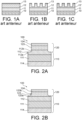
- a first part 112a of the second layer 112 is part of the base substrate 110 and a second part 112b of the second layer 112 is part of the mesas 120 (as shown in the figures 2A And 3A ).
- the mesas 120 are formed by etching the fourth layer 124, the third layer 123 and a first part 112a of the second doped layer 112 ( figures 2A And 3A ). By stopping the etching in the doped layer, the entire height of the third n++123 layer is available for relaxation.
- Each mesa 120 successively comprises from the base: the second part 112b of the layer 112 of doped GaN, the third layer 123 of heavily doped (Al,In,Ga)N and the fourth layer 124 of (Al,In,Ga)N undoped or lightly doped.
- the first part 112a of the second layer 112 of doped GaN protects the additional layer 113 during the porosification step. Thus, the additional layer 113 is not in contact with the solution.
- the first part of the doped GaN layer is a layer common to all mesas.
- the mesas 120 are formed by etching the fourth layer 124 and part of the heavily doped third layer 123 ( figures 2B And 3B ).
- the n++ doped layer 123 is not completely etched, thus preserving the integrity of the n-GaN layer.
- This mode embodiment is particularly advantageous for protecting the buried n++ doped layer 113 ( Figure 3B ).
- a first part 123a of layer 123 is in the base substrate 110 and a second part 123b of layer 123 is part of the mesas 120.
- the structuring of the stack is, for example, carried out by photolithography.
- a structure 100 comprising a base substrate 110 surmounted by a plurality of mesas 120 made of (Al,In,Ga)N/(Al,In,Ga)N.
- the mesas 120 are elements in relief. They are obtained, for example, by etching a continuous layer or several superimposed continuous layers, so as to leave only a certain number of "reliefs" of this layer or these layers.
- the etching is preferably carried out with a hard mask, for example SiO 2 .
- this hard mask is removed by a wet chemical process before porosification. It is also possible to remove this hard mask after porosification, by releasing it only, in the areas used for polarization for electrochemical polarization.
- the mask is removed before the porosification step.
- the sides of the mesas 120 are perpendicular to this stack of layers.
- the surface of the mesas can be circular, hexagonal, square or rectangular.
- the largest surface dimension of the mesas 120 ranges from 500nm to 500 ⁇ m.
- the largest dimension of a circular surface is the diameter.
- the spacing between two consecutive mesas 120 ranges from 50nm to 20 ⁇ m.
- the support layer 114 has, for example, a thickness ranging from 250 ⁇ m to 2mm.
- the thickness depends on the nature of the support layer 114 and its dimensions. For example, for a sapphire support layer 2 inches in diameter, the thickness can be 350 ⁇ m. For a support layer in 6 inch diameter sapphire, thickness can be 1.3mm. For a silicon support layer of 200mm in diameter, the thickness can be 1mm.
- the first layer 111 is a GaN nest layer. It is a layer not intentionally doped (nest) so as not to be porosified. By GaN not intentionally doped, we mean a concentration less than 5.10 17 at/cm 3 .
- the structure 100 and a counter electrode are electrically connected to a voltage or current generator.
- the device plays the role of working electrode (WE). Subsequently, it will be called a voltage generator, but it could be a current generator making it possible to apply a current between the device and the counter electrode.
- contact can be made on the base substrate 110.
- the resumption of contact can be made on the second layer 112 of doped GaN (the resumption of contact is represented by an arrow on the Figures 2A, 2B , 3A and 3B ).
- the resumption of contact can be made on the bottom of the mesas, at the level of the second layer 112, which makes it possible to use the etching step to also make the contacts.
- the electrodes are immersed in an electrolyte, also called an electrolytic bath or electrolytic solution.
- the electrolyte can be acidic or basic.
- the electrolyte is, for example, oxalic acid. It can also be KOH, HF, HNO 3 , NaNOs or H 2 SO 4 .
- the electrochemical anodization step can be carried out under ultraviolet (UV) light.
- UV ultraviolet
- the porosification obtained depends on the doping of the layer and the process parameters (applied voltage, duration, nature and concentration of the electrolyte, chemical post-treatment or annealing). The variation in porosification makes it possible to control the incorporation/segregation rate. Porosification, and in particular, the size of the pores, may vary subsequently, during the resumption of epitaxy depending on the temperature applied.
- the method comprises a subsequent step e) during which an epitaxy is carried out on the mesas 120, whereby an epitaxial layer is obtained which is at least partially relaxed, and preferably totally relaxed.
- the layer is 100% relaxed if ac 2 corresponds to the mesh parameter of the massive material, of the same composition as the re-epitaxial layer.
- the other part of the doped GaN layer is part of the base of the structure.
- a structure with 3 ⁇ m wide mesas and a structure with 5 ⁇ m wide mesas were manufactured.
- the mesa is entirely porosified but an edge/center effect of the mesas is still present. Furthermore, such a configuration can lead to integration problems with respect to thickness. Indeed, to porosify large mesas, the contact layer must be thicker. However, for a silicon substrate, it is not possible to have a thickness of 4 ⁇ m, which leads to integration problems.
- the electrolyte infiltrates through the defects ('V-pits') of the InGaN layer. Porosification takes place through this, thus porosifying the center of the mesa whatever the values of a and L. It is also possible to have an edge/center effect of the plate ('wafer') with porosification incomplete mesas located in the center of the plate due to the degradation of conductivity of the current injection layer during electrochemical polarization.
- a structure with mesas of 3 ⁇ m width and a structure with mesas of 5 ⁇ m width were fabricated.
- the porosification step is carried out by applying a voltage of 9V for 500s (non-pulsed) in an oxalic acid solution (0.3M).
Landscapes
- Led Devices (AREA)
- Thin Film Transistor (AREA)
- Insulated Gate Type Field-Effect Transistor (AREA)
Applications Claiming Priority (2)
| Application Number | Priority Date | Filing Date | Title |
|---|---|---|---|
| FR2212783A FR3142836B1 (fr) | 2022-12-05 | 2022-12-05 | Procédé de porosification de mésas (Al,In,Ga)N/(Al,In,Ga)N |
| EP23213631.7A EP4383359A1 (de) | 2022-12-05 | 2023-12-01 | Verfahren zur porenbildung von mesa aus (al,in,ga)n/(al,in,ga)n und entsprechende struktur |
Related Parent Applications (2)
| Application Number | Title | Priority Date | Filing Date |
|---|---|---|---|
| EP23213631.7A Division EP4383359A1 (de) | 2022-12-05 | 2023-12-01 | Verfahren zur porenbildung von mesa aus (al,in,ga)n/(al,in,ga)n und entsprechende struktur |
| EP23213631.7A Division-Into EP4383359A1 (de) | 2022-12-05 | 2023-12-01 | Verfahren zur porenbildung von mesa aus (al,in,ga)n/(al,in,ga)n und entsprechende struktur |
Publications (2)
| Publication Number | Publication Date |
|---|---|
| EP4394879A2 true EP4394879A2 (de) | 2024-07-03 |
| EP4394879A3 EP4394879A3 (de) | 2024-08-14 |
Family
ID=85727121
Family Applications (2)
| Application Number | Title | Priority Date | Filing Date |
|---|---|---|---|
| EP23213631.7A Pending EP4383359A1 (de) | 2022-12-05 | 2023-12-01 | Verfahren zur porenbildung von mesa aus (al,in,ga)n/(al,in,ga)n und entsprechende struktur |
| EP24174598.3A Pending EP4394879A3 (de) | 2022-12-05 | 2023-12-01 | Verfahren zur porosifizierung einer (al,in,ga)n schicht |
Family Applications Before (1)
| Application Number | Title | Priority Date | Filing Date |
|---|---|---|---|
| EP23213631.7A Pending EP4383359A1 (de) | 2022-12-05 | 2023-12-01 | Verfahren zur porenbildung von mesa aus (al,in,ga)n/(al,in,ga)n und entsprechende struktur |
Country Status (4)
| Country | Link |
|---|---|
| US (1) | US20240186445A1 (de) |
| EP (2) | EP4383359A1 (de) |
| CN (1) | CN118156379A (de) |
| FR (1) | FR3142836B1 (de) |
Families Citing this family (1)
| Publication number | Priority date | Publication date | Assignee | Title |
|---|---|---|---|---|
| FR3164057A1 (fr) * | 2024-06-27 | 2026-01-02 | Commissariat A L' Energie Atomique Et Aux Energies Alternatives | Procédé de porosification de mésas |
Family Cites Families (3)
| Publication number | Priority date | Publication date | Assignee | Title |
|---|---|---|---|---|
| EP3298624B1 (de) * | 2015-05-19 | 2023-04-19 | Yale University | Verfahren und vorrichtung für eine iii-nitrid-kantenemittierende laserdiode mit hohem begrenzungsfaktor mit gitterangepasster mantelschicht |
| FR3105567B1 (fr) * | 2019-12-19 | 2021-12-17 | Commissariat Energie Atomique | Procede pour fabriquer une structure gan/ingan relaxee |
| GB2593693B (en) * | 2020-03-30 | 2022-08-03 | Plessey Semiconductors Ltd | LED precursor |
-
2022
- 2022-12-05 FR FR2212783A patent/FR3142836B1/fr active Active
-
2023
- 2023-11-30 US US18/524,628 patent/US20240186445A1/en active Pending
- 2023-12-01 EP EP23213631.7A patent/EP4383359A1/de active Pending
- 2023-12-01 EP EP24174598.3A patent/EP4394879A3/de active Pending
- 2023-12-04 CN CN202311650739.2A patent/CN118156379A/zh active Pending
Non-Patent Citations (2)
| Title |
|---|
| APPL. PHYS. LETT., vol. 116, 2020, pages 111101 |
| PASAYAT ET AL., MATERIALS, vol. 13, 2020, pages 213 |
Also Published As
| Publication number | Publication date |
|---|---|
| US20240186445A1 (en) | 2024-06-06 |
| EP4394879A3 (de) | 2024-08-14 |
| FR3142836A1 (fr) | 2024-06-07 |
| CN118156379A (zh) | 2024-06-07 |
| FR3142836B1 (fr) | 2025-12-19 |
| EP4383359A1 (de) | 2024-06-12 |
Similar Documents
| Publication | Publication Date | Title |
|---|---|---|
| EP3840065B1 (de) | Verfahren zur herstellung einer entspannten gan/ingan-struktur und daraus resultierende struktur | |
| EP3840016A1 (de) | Verfahren zur herstellung eines substrats, das eine entspannte ingan-schicht umfasst | |
| FR3124312A1 (fr) | Procede pour fabriquer une matrice a emission native | |
| EP4105999B1 (de) | Verfahren zur herstellung einer nativen emissionsmatrix | |
| EP4362101B1 (de) | Diodenmatrixwachstumssubstrat mit mesas mit verschiedenen porenbildungsebenen | |
| EP4394879A2 (de) | Verfahren zur porosifizierung einer (al,in,ga)n schicht | |
| US20250318322A1 (en) | Method for manufacturing a substrate comprising a relaxed ingan layer and substrate thus obtained for the resumption of growth of a led structure | |
| EP4379800B1 (de) | Verfahren zur herstellung eines wachstumssubstrats mit unterschiedlichen elektrochemische porosifikationsebenen mit mesas mit unterschiedlichen porenbildungsgraden | |
| EP3836235A1 (de) | Verfahren zum aufbringen einer strukturierten materialschicht | |
| EP4521891A1 (de) | Verfahren zur porenbildung von mesa (al,in,ga)n/(al,in,ga)n | |
| FR3144413A1 (fr) | Procede de porosification de mésa facilitant la reprise de contact | |
| EP4679983A1 (de) | Verfahren zur herstellung einer photonischen vorrichtung und entsprechende photonische vorrichtung | |
| EP4672925A1 (de) | Verfahren zur porenbildung von mesas | |
| EP4391064B1 (de) | Verfahren zur herstellung von mikro-leds und resultierende struktur mit mikro-leds | |
| CN113013304B (zh) | 弛豫gan/ingan结构及其制造方法 | |
| EP4398317A1 (de) | Verfahren zur herstellung eines wachstumssubstrats mit mesas mit unterschiedlicher verformbarkeit durch elektrochemisches ätzen und porösmachung | |
| FR3143850A1 (fr) | Procédé de réalisation d’un dispositif électronique |
Legal Events
| Date | Code | Title | Description |
|---|---|---|---|
| PUAI | Public reference made under article 153(3) epc to a published international application that has entered the european phase |
Free format text: ORIGINAL CODE: 0009012 |
|
| STAA | Information on the status of an ep patent application or granted ep patent |
Free format text: STATUS: REQUEST FOR EXAMINATION WAS MADE |
|
| 17P | Request for examination filed |
Effective date: 20240507 |
|
| AC | Divisional application: reference to earlier application |
Ref document number: 4383359 Country of ref document: EP Kind code of ref document: P |
|
| AK | Designated contracting states |
Kind code of ref document: A2 Designated state(s): AL AT BE BG CH CY CZ DE DK EE ES FI FR GB GR HR HU IE IS IT LI LT LU LV MC ME MK MT NL NO PL PT RO RS SE SI SK SM TR |
|
| REG | Reference to a national code |
Ref country code: DE Ref legal event code: R079 Free format text: PREVIOUS MAIN CLASS: H01L0027150000 Ipc: H01L0033000000 |
|
| PUAL | Search report despatched |
Free format text: ORIGINAL CODE: 0009013 |
|
| AK | Designated contracting states |
Kind code of ref document: A3 Designated state(s): AL AT BE BG CH CY CZ DE DK EE ES FI FR GB GR HR HU IE IS IT LI LT LU LV MC ME MK MT NL NO PL PT RO RS SE SI SK SM TR |
|
| RIC1 | Information provided on ipc code assigned before grant |
Ipc: H01L 21/306 20060101ALN20240709BHEP Ipc: H01L 33/02 20100101ALN20240709BHEP Ipc: H01L 27/15 20060101ALI20240709BHEP Ipc: H01L 33/12 20100101ALI20240709BHEP Ipc: H01L 33/32 20100101ALI20240709BHEP Ipc: H01L 33/16 20100101ALI20240709BHEP Ipc: H01L 33/00 20100101AFI20240709BHEP |
|
| RIN1 | Information on inventor provided before grant (corrected) |
Inventor name: MEDJAHED, ILYES Inventor name: LEVY, FRANCOIS Inventor name: PERNEL, CAROLE Inventor name: AUDIBERT, MARGAUX |
|
| RAP3 | Party data changed (applicant data changed or rights of an application transferred) |
Owner name: COMMISSARIAT A L'ENERGIE ATOMIQUE ET AUX ENERGIESALTERNATIVES |