EP4391216A1 - Vorrichtung und system zum teilen und kombinieren von signalen im frequenzbereich - Google Patents
Vorrichtung und system zum teilen und kombinieren von signalen im frequenzbereich Download PDFInfo
- Publication number
- EP4391216A1 EP4391216A1 EP23214043.4A EP23214043A EP4391216A1 EP 4391216 A1 EP4391216 A1 EP 4391216A1 EP 23214043 A EP23214043 A EP 23214043A EP 4391216 A1 EP4391216 A1 EP 4391216A1
- Authority
- EP
- European Patent Office
- Prior art keywords
- waveguide
- frequency
- port
- previous
- signal
- Prior art date
- Legal status (The legal status is an assumption and is not a legal conclusion. Google has not performed a legal analysis and makes no representation as to the accuracy of the status listed.)
- Pending
Links
Images

Classifications
-
- H—ELECTRICITY
- H01—ELECTRIC ELEMENTS
- H01P—WAVEGUIDES; RESONATORS, LINES, OR OTHER DEVICES OF THE WAVEGUIDE TYPE
- H01P1/00—Auxiliary devices
- H01P1/20—Frequency-selective devices, e.g. filters
- H01P1/213—Frequency-selective devices, e.g. filters combining or separating two or more different frequencies
- H01P1/2138—Frequency-selective devices, e.g. filters combining or separating two or more different frequencies using hollow waveguide filters
-
- H—ELECTRICITY
- H01—ELECTRIC ELEMENTS
- H01P—WAVEGUIDES; RESONATORS, LINES, OR OTHER DEVICES OF THE WAVEGUIDE TYPE
- H01P1/00—Auxiliary devices
- H01P1/20—Frequency-selective devices, e.g. filters
- H01P1/213—Frequency-selective devices, e.g. filters combining or separating two or more different frequencies
- H01P1/2133—Frequency-selective devices, e.g. filters combining or separating two or more different frequencies using coaxial filters
-
- H—ELECTRICITY
- H01—ELECTRIC ELEMENTS
- H01P—WAVEGUIDES; RESONATORS, LINES, OR OTHER DEVICES OF THE WAVEGUIDE TYPE
- H01P1/00—Auxiliary devices
- H01P1/16—Auxiliary devices for mode selection, e.g. mode suppression or mode promotion; for mode conversion
- H01P1/161—Auxiliary devices for mode selection, e.g. mode suppression or mode promotion; for mode conversion sustaining two independent orthogonal modes, e.g. orthomode transducer
-
- H—ELECTRICITY
- H01—ELECTRIC ELEMENTS
- H01P—WAVEGUIDES; RESONATORS, LINES, OR OTHER DEVICES OF THE WAVEGUIDE TYPE
- H01P1/00—Auxiliary devices
- H01P1/165—Auxiliary devices for rotating the plane of polarisation
- H01P1/17—Auxiliary devices for rotating the plane of polarisation for producing a continuously rotating polarisation, e.g. circular polarisation
- H01P1/171—Auxiliary devices for rotating the plane of polarisation for producing a continuously rotating polarisation, e.g. circular polarisation using a corrugated or ridged waveguide section
-
- H—ELECTRICITY
- H01—ELECTRIC ELEMENTS
- H01P—WAVEGUIDES; RESONATORS, LINES, OR OTHER DEVICES OF THE WAVEGUIDE TYPE
- H01P3/00—Waveguides; Transmission lines of the waveguide type
- H01P3/12—Hollow waveguides
- H01P3/123—Hollow waveguides with a complex or stepped cross-section, e.g. ridged or grooved waveguides
-
- H—ELECTRICITY
- H01—ELECTRIC ELEMENTS
- H01P—WAVEGUIDES; RESONATORS, LINES, OR OTHER DEVICES OF THE WAVEGUIDE TYPE
- H01P5/00—Coupling devices of the waveguide type
- H01P5/12—Coupling devices having more than two ports
- H01P5/16—Conjugate devices, i.e. devices having at least one port decoupled from one other port
- H01P5/18—Conjugate devices, i.e. devices having at least one port decoupled from one other port consisting of two coupled guides, e.g. directional couplers
-
- H—ELECTRICITY
- H01—ELECTRIC ELEMENTS
- H01P—WAVEGUIDES; RESONATORS, LINES, OR OTHER DEVICES OF THE WAVEGUIDE TYPE
- H01P5/00—Coupling devices of the waveguide type
- H01P5/12—Coupling devices having more than two ports
- H01P5/16—Conjugate devices, i.e. devices having at least one port decoupled from one other port
- H01P5/19—Conjugate devices, i.e. devices having at least one port decoupled from one other port of the junction type
-
- H—ELECTRICITY
- H01—ELECTRIC ELEMENTS
- H01Q—ANTENNAS, i.e. RADIO AERIALS
- H01Q1/00—Details of, or arrangements associated with, antennas
- H01Q1/50—Structural association of antennas with earthing switches, lead-in devices or lightning protectors
Definitions
- Examples of the present disclosure relate to an apparatus and system for splitting and combining signals in the frequency domain. Some examples, though without prejudice to the foregoing, relate to a waveguide junction for splitting and combining signals in the frequency domain and a diplexer comprising the same.
- a waveguide junction that enables a compact duplexing solution. In some circumstances it can be desirable to provide a waveguide junction that avoids the need for a filter (a "filter-less waveguide). In some circumstances it can be desirable to provide a frequency splitting waveguide junction that enables a first signal having a (wide) first frequency band to be split into second and third signals of a particular/selected (narrow) second and third frequency bands which are sub-bands of the first frequency band. In some circumstances it can be desirable to provide a frequency combining waveguide junction that enables second and third signals of a particular/selected second and third frequency bands, which are sub-bands of a first frequency band, to be combined into a first signal having the first frequency band.
- an apparatus comprising:
- a waveguide junction a diplexer, an OrthoMode Transducer or an antenna system comprising the apparatus.
- examples of the disclosure there is provided a method of providing and/or manufacturing an apparatus and/or system as described herein.
- the third waveguide port is configured to have a cut-off operational frequency that is higher than an upper frequency the operational frequency band of the second waveguide port.
- the waveguide structure is arranged at an oblique angle relative to one or more of the waveguide ports.
- a length of a diagonal of the cross-sectional shape of the waveguide structure is greater than or equal to a width of the first and/or second waveguide ports.
- the waveguide structure comprises one or more ridges configured to select a frequency at which the first signal is split in the frequency domain.
- the waveguide structure comprises one or more spline-based shapes configured to enhance the RF performance of the apparatus.
- the second and third waveguide ports are arranged parallel to one another.
- the second and third waveguide ports have a separation distance approximately equal to 1/16 th of a wavelength of an upper frequency of the third frequency band of operation.
- the apparatus a waveguide junction
- a similar feature may be referenced by the same three-digit number.
- an optional subscript to the three-digit number can be used to differentiate different instances of similar features. Therefore, a three-digit number without a subscript can be used as a generic reference and the three-digit number with a subscript can be used as a specific reference.
- a subscript can comprise a single digit that labels different instances.
- a subscript can comprise two digits including a first digit that labels a group of instances and a second digit that labels different instances in the group.
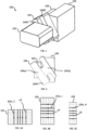
- FIG. 1 shows a perspective view of an example of an apparatus 100 according to the present disclosure.
- the apparatus is a wave guide component, such as a waveguide junction for splitting/combining Radio Frequency, RF, signals in the frequency domain.
- the apparatus comprises: a first waveguide port 101, a second waveguide port 102 and a third waveguide port 103; each of which is substantially aligned in the same direction (i.e. are substantially parallel to one another - as compared to a T-junction where a first port is at right angles for a second and a third port).
- the apparatus also comprises a waveguide structure 104 that is disposed between the first waveguide port and the second and third waveguide ports.
- the first waveguide port 101 serves as an input/output, I/O, port for supporting a first signal 101s (see FIG. 3A ).
- the first waveguide port is configured to have a first frequency band of operation.
- the first waveguide port may be dimensioned so as to have a frequency band of operation that corresponds to the first frequency band.
- the first signal which may also be referred to as a common signal "C" is a wideband signal having a frequency band that corresponds to the first frequency band.
- the second waveguide port 102 serves as an input/output, I/O, port for supporting a second signal 102s (see FIG. 3B ).
- the second waveguide port is configured to have a second frequency band of operation, wherein the second frequency band of operation is a sub-band of the first frequency band of operation.
- the second signal which may also be referred to as a low signal "L" is a narrow signal having a frequency band that corresponds to a lower sub-band portion of the first frequency band.
- the third waveguide port 103 serves as an input/output, I/O, port for supporting a third signal 103s (see FIG. 3C ).
- the third waveguide port is configured to have a third frequency band of operation, wherein the third frequency band of operation is a sub-band of the first frequency band of operation and is different to the second frequency band of operation.
- the third signal which may also be referred to as a high signal "H" is a narrow signal having a frequency band that corresponds to a higher sub-band portion of the first frequency band.
- the waveguide structure 104 comprises first and second opposing faces 104f1 and 104f2.
- the waveguide structure is sandwiched between the ports such that the first face is disposed adjacent the first port, and the second face is adjacent the second and third waveguide ports.
- the waveguide structure 104 serves as a frequency selector and frequency splitter (i.e. selecting the frequency at which the first signal is split) which separates one wide frequency band from one rectangular waveguide towards two different rectangular waveguides operating each one with a new frequency sub band.
- the new frequency sub bands do not have to be the same in terms of fractional bandwidth.
- the waveguide structure provides flexibility regarding the adjustment of the fractional bandwidth for each new frequency sub band.
- the apparatus also enables frequency discrimination (i.e. low and high bands in the second and third waveguide ports) without the use of a filter.
- FIG. 2 shows a front-on end view of the apparatus 100 but wherein, for clarity, the first port is not shown.
- the waveguide structure has an asymmetric cross-sectional shape (i.e. the waveguide structure is a asymmetric cross-sectional hollow shape) which comprises/definiens:
- the dimensions of the first aperture region are larger than those of the second aperture region such that the extent/size of the first aperture region defines a larger contiguous cross-sectional area than that of the second aperture region.
- the first aperture region can be considered as the portion of the waveguide structure on one side of the waveguide structure (in this example to the left of the illustrated bisecting dotted line - i.e. the upper and lower limbs/legs of the left hand side of the H-shaped structure), and the second aperture region can be considered as the portion of the waveguide structure on this other side (i.e. to the right of the bisecting dotted line which corresponds to the upper and lower limbs/legs of the right hand side of the H-shaped structure).
- the example of the waveguide structure of FIGs 1 and 2 consists of a central waveguide shaped like an H, with rounded corners and one side (a left side defining the first aperture region) thicker than the other side (the right side defining the second aperture region). This allows a low frequency sub-band to be directed through the wider part of the H, and a high frequency sub-band through the thinner part of the H.
- the waveguide structure is oriented at an angle, e.g. 45°, to urge the polarized wave towards the output waveguide ports.
- One or more inclusions or ridged shapes can also be used to adapt each frequency band. It is to be appreciated that the length and width of each ridges can be optimized (e.g. using a genetic algorithm) in order to enhance the splitting effect of the waveguide structure and control/adjust/select the frequency at which the common signal is split.
- the waveguide structure is arranged (i.e. configured/disposed/orientated) relative to the second and third waveguide ports such that:
- the waveguide structure is configured such that the majority of its larger first aperture region overlies/lies in front of the smaller third waveguide port, and the majority of the waveguide structure's smaller second aperture region overlies/lies in front of the larger second waveguide port.
- more of the larger first aperture region overlies the smaller third waveguide port than the larger second waveguide; and likewise more of the smaller second aperture region overlies the larger second waveguide port than the smaller first waveguide port.
- the first waveguide port is substantially coaxially aligned with the waveguide structure, i.e. their centres/centroids are substantially aligned with one another.
- the second and third waveguide ports are arranged so that their respective centres/centroids are as close to the centre/centroid of the waveguide structure as possible.
- the first signal 101s, C has a first polarisation state p1 (e.g. vertically polarised E-field), whereas the second and third signals 102s, Land 103s, H have a second polarisation state p2 (e.g. horizontally polarized E-field - at 90° to p1).
- first polarisation state p1 e.g. vertically polarised E-field
- second and third signals 102s, Land 103s, H have a second polarisation state p2 (e.g. horizontally polarized E-field - at 90° to p1).
- the first waveguide port 101 may be a rectangular waveguide supporting a TE10 mode and the propagation of a first signal 101s, C having a vertical polarisation p1.
- the first waveguide port is configured to have a first frequency cut off, e.g. 4.75 Ghz, that is chosen to transmit a RF signal over a wide frequency band (e.g. between 5.5 GHz and 9 GHz) -of course other frequencies could be selected.
- the second waveguide port 102 may be a rectangular waveguide supporting a TE10 mode and the propagation of a second signal 102s, L having a horizontal polarisation p2.
- the second waveguide port may have a second frequency cut off the same as or close to that of the first waveguide port, e.g. 4.5 GHz (of course other frequencies could be selected), and it is configured to convey a lower frequency sub-band as compared to the third waveguide port.
- the second waveguide port is thereby associated with conveying low-band LB signals.
- the third waveguide port 103 may be a rectangular waveguide supporting a TE10 mode and the propagation of a third signal 103s, H having a horizontal polarisation p2.
- the third waveguide port may have a third frequency cut off that is higher than an upper frequency of the operational frequency band of the second waveguide port, e.g. 7.25 GHz (of course other frequencies could be selected) and it is configured to convey a higher frequency sub-band as compared to the second waveguide port.
- the third waveguide port is thereby associated with conveying high-band HB signals.
- the dimensions of the three waveguide ports/waveguide just before and after the H-shape waveguide structure also affect the frequency splitting functionality.
- the smaller waveguide 103 impacts the high frequency sub-band selection.
- the waveguide structure is configured to rotate the polarisations of the signals between the first and second polarisation states.
- the waveguide structure may serve as a polarisation rotator and also as a frequency splitter.
- the first wideband signal C input via the first waveguide port and having a vertical polarisation, undergoes 90° polarisation rotation and frequency splitting via the waveguide structure resulting in: a second signal L output via the second waveguide port, and a third signal H output via the third waveguide port - both having a horizontal polarisation.
- a second signal L input via the second waveguide port, and a third signal H input via the third waveguide port, both having a horizontal polarisation undergo 90° polarisation rotation and combination via the waveguide structure resulting in a first wideband signal C having a vertical polarisation output via the first waveguide port.
- the wave guide structure can be considered as being a 90° polarisation rotator albeit with substantial modifications, namely in relation to its shape (not least its asymmetric shape with differing sized aperture portions and the use of ridges as discussed further below), as well as its respective positioning and alignment with respect to first, second and third waveguide ports.
- Conventional polarisation rotators only direct one polarisation at a time.
- two TE10 polarisations on two rectangular waveguides 102 and 103 operating in two different frequency bands are directed to from a single TE10 signal propagating in a common rectangular waveguide 101.
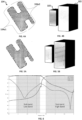
- FIGs 4A and 4B, and 5A and 5B schematically illustrate simulations of E-field distribution in the waveguide structure 104 ( FIGS 4A and 5A , respectively at a low band mid frequency point and a high band mid frequency point) and the second and third wave guide ports ( FIGS 4B and 5B , respectively at a low band mid frequency point and a high band mid frequency point).
- FIGs 4A and 5A schematically illustrate simulations of E-field distribution in the waveguide structure 104 ( FIGS 4A and 5A , respectively at a low band mid frequency point and a high band mid frequency point) and the second and third wave guide ports ( FIGS 4B and 5B , respectively at a low band mid frequency point and a high band mid frequency point).
- FIGs show that the high and low frequency sub-bands are correctly split and conveyed to the low and high band waveguide ports (i.e. the second and third waveguide ports) depending on the signal frequency.
- FIGs 4A and 4B schematically illustrate the E-filed distribution at a low band mid frequency point (e.g. 6.425 GHz). As shown, almost all the signal is transmitted in the LB waveguide port 102 by virtue of the cut-off frequency of the HB waveguide port 103.
- a low band mid frequency point e.g. 6.425 GHz
- FIGs 5A and 5B schematically illustrate the E-filed distribution at a high band mid frequency point (e.g. 8.1 GHz).
- the signal is rightly transmitted in the HB waveguide 103.
- FIG. 6 illustrate simulation results (simulated S-parameters) which show that a first signal is well split into two sub-bands: one from 5.9 GHz to 7.2 GHz, and the other from 7.5 GHz to 9 GHz. Whilst these performances may not be optimal, they do show the functionality and feasibility of the waveguide structure in effecting signal splitting. As will be discussed below, the waveguide structure can be modified/improved to enhance its Return Loss, RL, characteristics.
- the waveguide structure's shape is not limited to an 'H' based shape. Various configurations are possible.
- FIG. 7 illustrates an example of an alternatively shaped waveguide structure 104, namely in the form of two offset square-rounded waveguide sections.
- the waveguide structure again has an asymmetric shape, with a first aperture region 104a1 being larger in extent/size than a second aperture region 104a2.
- One key point of the design is the length of the diagonal(s) 104d, this/these must be large enough to allow a wave to rotate (i.e. the diagonals must be equal to or wider than the widest waveguide port (e.g. the width of the first or second waveguide ports).
- the cross-sectional shape of the waveguide structure could be modified so as to include one or more a genetic algorithm-based curves or splines in order to add smoothness in the shape of the wave guide structure and thus enhance the bandwidth.
- the location of the one or more spline-based shapes within the waveguide structure and/or one or more dimensions of the one or more spline-based shapes can be optimised to enhance the RF performance.
- FIG. 8 illustrates a further example of a waveguide structure 104, which is based on an H-shape albeit with enhancements.
- the H-shaped waveguide structure has been optimized to improve its RF performance (improvement of Return Loss, Insertion Loss and Inter-band Rejection).
- the H-shape is modified by using spline-based shapes (random analytic curves).
- the waveguide structure is arranged at an oblique angle ( ⁇ ) relative to the third and second waveguide ports (which are parallel to one another).
- ⁇ oblique angle
- the cross-sectional shape of the waveguide structure is elongate defining a longitudinal axis of the waveguide structure.
- the cross-sectional shape of the second or third waveguide port is elongate defining a longitudinal axis of the second or third waveguide port.
- the waveguide structure is arranged relative to the second or third waveguide port such that the longitudinal axis of the waveguide structure is at a predetermined angle ( ⁇ ) to the longitudinal axis of the second or third waveguide port, wherein the redetermined angle may be an oblique angle, such as between 25 to 45 degrees, an angle of approximately 35 degrees, or an angle of approximately 45 degrees.
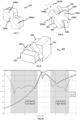
- FIG. 9 shows another example of an apparatus 100 comprising the waveguide structure 104 of FIG. 8 sandwiched between the first waveguide port 101 and the second and third waveguide ports 102 and 103 (wherein such waveguide ports may correspond to those as discussed above, i.e. with the second waveguide port being configured to convey LB frequency signals and the third waveguide port being configured to convey HB frequency signals, wherein the LB and HB are sub bands of a frequency band supported by the first waveguide port).
- random analytic curves may allow more efficient selection/discrimination of frequency sub-bands. They may also improve the return loss of the apparatus. Indeed, the rounded shapes may permit a smoother propagation of the signal in the apparatus and reduce the risk of lowering the Return Loss figure.
- Examples of the disclosure may use a waveguide structure with a variable shape, optimized by means of a genetic algorithm.
- the shape of the waveguide structure can be square, round, rectangular, or randomly parametrized.
- Various simulations performed by the inventors have established that different waveguide structure shapes can work, by reusing existing polarization rotators structures, such as a bone-shape rotator (i.e. similar to FIG. 7 ). It has been found that optimal results are obtained using spline-based H shapes (such as in FIG. 8 .
- the optimized shape remains easily machinable, resulting in lower cost with standard machining process.
- an optimal waveguide structure may be an extruded H-shaped waveguide, whose diagonal is wider than the width of the largest waveguide port.
- a theta rotation of 35° ⁇ 10° with respect to a vertical axis (or 55° ⁇ 10° with respect to a horizontal axis) from the common rectangular waveguide is applied in order to get an optimal frequency operation.
- the apparatus of examples of the present disclosure allows all the waveguides ports to be put in the same direction (instead of a right angle often encountered in the state of the art). This may significantly reduce a size of the apparatus and device (e.g. diplexer/OMT/antenna system comprising the apparats). Furthermore, unlike other waveguide junctions; advantageously, waveguide junctions in accordance with the present disclosure do not require any kind of filter.
- FIG. 10 illustrates simulation results for the apparatus/waveguide junction of FIG. 9 .
- This shows that a common signal is well split into two sub-bands: the first from 5.8 GHz to 7.14 GHz, and the second from 7.74 GHz to 8.67 GHz.
- the Return Loss of the apparatus/waveguide junction has been significantly improved as compared to that of the apparatus/waveguide junction of FIG. 1 , better than 25 dB over almost all the sub-bands which demonstrates an excellent performance of the apparatus/waveguide junction of FIG. 9 .
- FIG. 11 shows the apparatus 100 along with further waveguiding components that are comprised in first and second waveguide pathways 201, 301.
- the first and second waveguide pathways respectively convey the L frequency sub-band signal and the H frequency sub-band signal to/from the second and third waveguide ports 102 and 103 respectively.
- FIG. 11 also shows that there is a separation distance between the second and third ports (and likewise between the first and second radio pathways) referred to as a septum distance, D septum .
- Stepped impedance waveguide sections 201 and 301 are added for the low and high bands, to obtain waveguide sizes matching with, for example R84_W112 and R70_WR137 standards.
- These waveguide sections made of quarter wavelength impedance transformers, also improve the rejection between the frequency bands. Thereby also improving a RL of a whole frequency divider system (i.e. which comprises the apparatus and waveguide pathways).
- a specific parameter D septum corresponds to a distance between the two waveguides right after the waveguide structure 104 (i.e. a separation distance between the second and third ports).
- the value of D septum is determined so as to satisfy multiple criteria:
- an optimal value of D septum is about one sixteenth of the guided wavelength ⁇ g at the desired frequency.
- the guided wavelength ⁇ g may correspond to an upper frequency of the higher sub-band (i.e. D septum may be approximately equal to 1/16th of a wavelength of an upper frequency of the third frequency band of operation).
- D septum is as small as possible while still allowing for machining.
- one-sixteenth of a guided wavelength relative to the upper frequency of the higher sub-band has been found to be an optimal compromise.
- each split signal (L and H) is conveyed through impedance matching made by ⁇ /4 (being ⁇ the free space wavelength) transformer sections of each radio pathway adapted for each frequency sub-band. As discussed above, this is done to increase the RF rejection between the frequency sub-bands. Also, it enables an adjustment of the dimensions of each radio pathway's waveguide so as to enable connection to standard size waveguides.
- Additional components are required to space the first and second waveguide pathways from each other, and to allow connection of RF measurement equipment.
- genetic-algorithm optimized right angle waveguides can be used for High band and Low band operation. They are optimized to present a best possible RL. They also allow some design flexibility to get the correct spacing of the device without lowering the RF performance.
- FIG. 12 A general view of the frequency splitter junction followed by the step impedance waveguides and the right-angle waveguides is illustrated FIG. 12 .
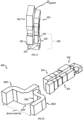
- FIG. 12 shows the apparatus 100 along with right angle waveguides that are comprised in first and second waveguide pathways 201, 301.
- the further waveguiding components of each waveguide pathway 201, 301 comprise two 90° elbows (i.e. a pair of 90° elbows for each waveguide pathway: 202i & 202ii, and 302i & 302ii. Two such elbows are provided to each radio pathway in order to adjust/regulate the distance between the two output ports (i.e. adjust the spacing of the device so as to enable the device to be connectable with standard size waveguides).
- a center distance to connect waveguide which corresponds to the spacing of the device, is controlled by the length of the right-angle waveguides. Hence, it is possible to shorten or lengthen the device spacing depending on the mechanical constraints of the environment.
- FIG. 13 shows the device of FIG. 12 further with a 90° polarization rotator per frequency sub band, 203 and 303, to re-orient the final waveguide section/ports 204 and 304 so as to be in the same direction as the common rectangular waveguide port 101.
- the performance of each rotator is set to maximize the RL on each defined sub-band.
- a dual-polarized dual-band antenna solution is a way for reducing the tower leasing cost, installation time and for lightening the tower structure.
- the system 400 may provide a filter-less waveguide frequency splitter solution for an antenna providing high radiofrequency performances.
- the system acts like a compact diplexing solution, easily adjustable for every targeted frequency bands.
- the system 400 may provide a filter-less waveguide frequency splitter that embodies two functions, namely a waveguide junction and a filtering solution, of a common diplexing solution in one element.
- the filter-less waveguide frequency splitter 400 has a similar architecture to certain conventional diplexers references, excepting that it does not contain/use any filter or tuning procedure. It consists of a frequency splitter junction (apparatus 100) and radio paths for each frequency sub-band 201, 301 (including straight and elbow waveguide sections) that are optimized to minimize the overall footprint of the device and enhance the RF performance.
- a stepped impedance waveguide is used per frequency sub-band to adjust the dimensions of the output guides and to enhance the rejection between frequency sub-bands.
- a signal of the common port 101 conveys both low band and high band frequencies.
- the two frequency sub-bands are split in the LB and HB waveguides 201 and 301 respectively so low band frequency is redirected at one port 102 and high frequency band at the other RF port 103.
- Two 90° polarisation rotators 203 and 303 are integrated into the system 400.
- Each polarisation rotator allows a RF signal guided in a rectangular waveguide to be rotated in its polarization direction in TE10 mode over a wide frequency band.
- a TE10 mode signal propagated in the waveguide of each radio pathway is rotated using the 90° polarisation rotator to an orthogonal waveguide port 204.
- the rotation requires two rectangular guides separated by a variable shape component (e.g. bone shaped component for each of 203 and 303) shown here as two rounded squares.
- a variable shape component e.g. bone shaped component for each of 203 and 303
- This shape allows a smooth and gradual rotation of the electric field from one waveguide to the other, resulting in a wide operating bandwidth and satisfactory S-parameters performance.
- simulations show the 90° polarisation rotator exhibiting a 30 dB simulated Return Loss over a 20% bandwidth (5.8 GHz - 7.4 GHz).
- the system 400 of FIG. 13 may form a diplexer 400 (such as may be used with an Otho-Mode Transducer of dual polarized and dual-band antenna system 500 as shown in FIG. 14 and discussed below).
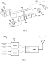
- FIG. 14 shows a dual band, dual polarization antenna system 500 which comprises a broadband and/or dual-band antenna feed, an Orthomode Transducer (OMT) and two diplexers (i.e. as per the system 400 of FIG. 13 ).
- OMT Orthomode Transducer
- Each diplexer splits, in the frequency domain, a radio frequency (RF) signal operating in a wide frequency band into two different and narrow frequency bands (and vice versa as a diplexer has the same RF properties transmitting or receiving).
- RF radio frequency
- One of the diplexers is associated with a Vertical polarization and the other diplexer is associated with the Horizontal polarization, FIG. 14 .
- FIG. 15 illustrates a manufacturing solution for the individual parts of the system of FIG. 13 .
- manufacture of the parts can be realized by other methods, not least such as additive manufacturing or sintering.
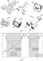
- the simplicity and compactness of the system of FIG. 13 permit the manufacturing, by classical machining, of the system in only two distinct layers, i.e. the bottom and top part of the waveguide pathways (as per the: top left and top centre images) that can be assembled together with the remaining unit elements, i.e. the splitter junction; Low Band output port; and High Band output port (as per the: top right, bottom left and bottom centre images) to form the overall assembled filter-less waveguide frequency splitter system 400 (as per the bottom right image).
- FIG. 16 a plot of simulated S-parameters of the filter-less waveguide frequency splitter system. This shows that the system's return loss in operating microwave frequency bands having a return loss value better than 20dB on both the low sub band and high sub band channels.
- the frequency splitter system operates a sub-band separation between 5.8 GHz and 7.14 GHz (23% relative bandwidth) for the lower band, and between 7.76 GHz and 8.68 GHz (12% relative bandwidth) for the higher band.
- an aim of examples of filter-less waveguide frequency splitter systems according to the present disclosure is to achieve a frequency band separation rather than necessarily a good rejection, as the latter can be provided by an upstream Outdoor Unit (ODU).
- ODU upstream Outdoor Unit
- FIG. 17 illustrates a plot of simulated reflection coefficients at each port of the filter-less waveguide frequency splitter system:
- FIG. 17 illustrates a plot of simulated Insertion Loss, IL, for each port of the filter-less waveguide frequency splitter system, taking into account Aluminium conductor as material, roughness 0.8 ⁇ m, Fig.19. This shows excellent IL values, better than 0.05 dB for the lower band and 0.2 dB for the higher band.
- examples of frequency splitting junctions and diplexers according to the present disclosure are more flexible as they do not rely on/require T-junction or Y-junction dimensioning and filter design (and hence examples can be narrower/have a reduced device separation distance). Also, instead of designing and optimising plural specific elements, examples are based on a single component: the frequency splitter/selector junction (i.e. apparatus 100). Knowing that only the dimensioning of the junction is mandatory, one can quickly and easily modify a frequency band of operation, especially since only the cut-off frequency must be calculated for the high band (i.e. the third waveguide port).
- the design of a frequency splitting junction may be more compact than existing solutions. Furthermore, there is no tuning process needed with any external assembly part (such as tuning screws for example). Examples of the present disclosure may thereby provide an improved frequency splitting/selecting junction that may give rise to advantages in reducing device size, weight, and manufacturing time (and hence costs).
- examples of the present disclosure can be used in combination with other devices.
- examples can be used in association with an OMT to reduce the number of devices and the complexity of the overall antenna system.
- features have been described with reference to certain examples, those features can also be present in other examples whether described or not. Accordingly, features described in relation to one example/aspect of the disclosure can include any or all of the features described in relation to another example/aspect of the disclosure, and vice versa, to the extent that they are not mutually inconsistent.
- the wording 'connect', 'couple' and 'communication' and their derivatives mean operationally connected/coupled/in communication. It should be appreciated that any number or combination of intervening components can exist (including no intervening components), i.e. so as to provide direct or indirect connection/coupling/communication. Any such intervening components can include hardware and/or software components.
- references to "a/an/the” [feature, element, component, means ...] are used with an inclusive not an exclusive meaning and are to be interpreted as "at least one" [feature, element, component, means ...] unless explicitly stated otherwise. That is any reference to X comprising a/the Y indicates that X can comprise only one Y or can comprise more than one Y unless the context clearly indicates the contrary. If it is intended to use 'a' or 'the' with an exclusive meaning then it will be made clear in the context. In some circumstances the use of 'at least one' or 'one or more' can be used to emphasise an inclusive meaning but the absence of these terms should not be taken to infer any exclusive meaning.
- the presence of a feature (or combination of features) in a claim is a reference to that feature (or combination of features) itself and also to features that achieve substantially the same technical effect (equivalent features).
- the equivalent features include, for example, features that are variants and achieve substantially the same result in substantially the same way.
- the equivalent features include, for example, features that perform substantially the same function, in substantially the same way to achieve substantially the same result.
- the apparatus described can alternatively or in addition comprise an apparatus which in some other examples comprises a distributed system of apparatus, for example, a client/server apparatus system.
- a distributed system of apparatus for example, a client/server apparatus system.
- each apparatus forming a component and/or part of the system provides (or implements) one or more features which collectively implement an example of the present disclosure.
- an apparatus is re-configured by an entity other than its initial manufacturer to implement an example of the present disclosure by being provided with additional software, for example by a user downloading such software, which when executed causes the apparatus to implement an example of the present disclosure (such implementation being either entirely by the apparatus or as part of a system of apparatus as mentioned hereinabove).
Landscapes
- Control Of Motors That Do Not Use Commutators (AREA)
Applications Claiming Priority (1)
| Application Number | Priority Date | Filing Date | Title |
|---|---|---|---|
| FI20226151 | 2022-12-22 |
Publications (1)
| Publication Number | Publication Date |
|---|---|
| EP4391216A1 true EP4391216A1 (de) | 2024-06-26 |
Family
ID=89076235
Family Applications (1)
| Application Number | Title | Priority Date | Filing Date |
|---|---|---|---|
| EP23214043.4A Pending EP4391216A1 (de) | 2022-12-22 | 2023-12-04 | Vorrichtung und system zum teilen und kombinieren von signalen im frequenzbereich |
Country Status (3)
| Country | Link |
|---|---|
| US (1) | US20240213642A1 (de) |
| EP (1) | EP4391216A1 (de) |
| CN (1) | CN118249061A (de) |
Families Citing this family (1)
| Publication number | Priority date | Publication date | Assignee | Title |
|---|---|---|---|---|
| CN118970402A (zh) * | 2024-08-20 | 2024-11-15 | 电子科技大学 | 一种基于两路等功率激励奇对称电场的高次模抑制过渡 |
Citations (3)
| Publication number | Priority date | Publication date | Assignee | Title |
|---|---|---|---|---|
| CN206585042U (zh) * | 2017-02-13 | 2017-10-24 | 广东通宇通讯股份有限公司 | 微波高频段极化转换器 |
| WO2021083498A1 (en) * | 2019-10-29 | 2021-05-06 | European Space Agency | Waveguide component for use in an orthomode junction or an orthomode transducer |
| WO2022086850A1 (en) * | 2019-10-18 | 2022-04-28 | Lockheed Martin Corporation | Reflector antenna with minimal focal distance and low cross-polarization |
-
2023
- 2023-12-04 EP EP23214043.4A patent/EP4391216A1/de active Pending
- 2023-12-13 US US18/538,288 patent/US20240213642A1/en active Pending
- 2023-12-20 CN CN202311759692.3A patent/CN118249061A/zh active Pending
Patent Citations (3)
| Publication number | Priority date | Publication date | Assignee | Title |
|---|---|---|---|---|
| CN206585042U (zh) * | 2017-02-13 | 2017-10-24 | 广东通宇通讯股份有限公司 | 微波高频段极化转换器 |
| WO2022086850A1 (en) * | 2019-10-18 | 2022-04-28 | Lockheed Martin Corporation | Reflector antenna with minimal focal distance and low cross-polarization |
| WO2021083498A1 (en) * | 2019-10-29 | 2021-05-06 | European Space Agency | Waveguide component for use in an orthomode junction or an orthomode transducer |
Also Published As
| Publication number | Publication date |
|---|---|
| US20240213642A1 (en) | 2024-06-27 |
| CN118249061A (zh) | 2024-06-25 |
Similar Documents
| Publication | Publication Date | Title |
|---|---|---|
| CN1284266C (zh) | 多信道馈送网络 | |
| WO2019223222A1 (zh) | 一种双极化双工天线及其构成的双频基站天线阵列 | |
| CN107425272B (zh) | 滤波天线阵列 | |
| CN110600875B (zh) | 具有高选择性的低剖面、紧凑型线极化及圆极化滤波天线 | |
| EP3583661B1 (de) | Kompaktes duales zirkulares polarisations-mehrbandwellenleiter-speisenetzwerk | |
| CN110943294B (zh) | 宽带低剖面双圆极化平板天线 | |
| TWI694635B (zh) | 三頻帶饋送組合件系統及方法 | |
| US20240213642A1 (en) | Apparatus and system for splitting and combining signals in the frequency domain | |
| CN116581550B (zh) | 一种馈源组件及馈源系统 | |
| CN104134836B (zh) | 一种基于四分之一波长短路馈线的平面双工器 | |
| CN115241643B (zh) | 基于K、Ka波段的高隔离度双圆极化天线 | |
| CN113097678B (zh) | 一种双频双极化分路器 | |
| CN114188688B (zh) | 一种小型化同轴波导正交模耦合器 | |
| CN109494485B (zh) | 一种宽带隔板圆极化器 | |
| Zhang et al. | Design of K/Ka-band diplex circular polarizer with high isolation | |
| Lin et al. | Filtering in-band full-duplex slot antenna based on TM 120 and TM 210 dual-mode resonators | |
| CN108879042B (zh) | 一种基于环形多模谐振器的三通带带通滤波器 | |
| US8929699B2 (en) | Symmetrical branching ortho mode transducer (OMT) with enhanced bandwidth | |
| CA3049208C (en) | High-q dispersion-compensated parallel-plate diplexer | |
| WO2024108397A1 (en) | Tuning element module for a modular waveguide junction | |
| CN204067528U (zh) | 一种基于四分之一波长短路馈线的平面双工器 | |
| CN116349085B (zh) | 用于对极化波进行复用或解复用的设备 | |
| CN120184549A (zh) | 一种Ka频段双极化四端口微波组件 | |
| Du et al. | Millimeter Wave Passive Frequency Routing Technique for Low-Cost Multi-Band Selectable Transceiver Systems | |
| TWI523416B (zh) | 埋藏式多頻帶通濾波器 |
Legal Events
| Date | Code | Title | Description |
|---|---|---|---|
| PUAI | Public reference made under article 153(3) epc to a published international application that has entered the european phase |
Free format text: ORIGINAL CODE: 0009012 |
|
| STAA | Information on the status of an ep patent application or granted ep patent |
Free format text: STATUS: THE APPLICATION HAS BEEN PUBLISHED |
|
| AK | Designated contracting states |
Kind code of ref document: A1 Designated state(s): AL AT BE BG CH CY CZ DE DK EE ES FI FR GB GR HR HU IE IS IT LI LT LU LV MC ME MK MT NL NO PL PT RO RS SE SI SK SM TR |
|
| STAA | Information on the status of an ep patent application or granted ep patent |
Free format text: STATUS: REQUEST FOR EXAMINATION WAS MADE |
|
| 17P | Request for examination filed |
Effective date: 20241216 |
|
| RAP3 | Party data changed (applicant data changed or rights of an application transferred) |
Owner name: NOKIA SOLUTIONS (SHANGHAI) CO., LTD. |
|
| STAA | Information on the status of an ep patent application or granted ep patent |
Free format text: STATUS: THE APPLICATION HAS BEEN WITHDRAWN |