EP4397784A1 - Dünnschichtabscheidungsvorrichtung, dünnschichtabscheidungsverfahren und dünnschichtabscheidungsvorrichtung - Google Patents
Dünnschichtabscheidungsvorrichtung, dünnschichtabscheidungsverfahren und dünnschichtabscheidungsvorrichtung Download PDFInfo
- Publication number
- EP4397784A1 EP4397784A1 EP22863574.4A EP22863574A EP4397784A1 EP 4397784 A1 EP4397784 A1 EP 4397784A1 EP 22863574 A EP22863574 A EP 22863574A EP 4397784 A1 EP4397784 A1 EP 4397784A1
- Authority
- EP
- European Patent Office
- Prior art keywords
- substrate
- thin film
- film deposition
- processing chamber
- heating tray
- Prior art date
- Legal status (The legal status is an assumption and is not a legal conclusion. Google has not performed a legal analysis and makes no representation as to the accuracy of the status listed.)
- Pending
Links
Images



















Classifications
-
- C—CHEMISTRY; METALLURGY
- C23—COATING METALLIC MATERIAL; COATING MATERIAL WITH METALLIC MATERIAL; CHEMICAL SURFACE TREATMENT; DIFFUSION TREATMENT OF METALLIC MATERIAL; COATING BY VACUUM EVAPORATION, BY SPUTTERING, BY ION IMPLANTATION OR BY CHEMICAL VAPOUR DEPOSITION, IN GENERAL; INHIBITING CORROSION OF METALLIC MATERIAL OR INCRUSTATION IN GENERAL
- C23C—COATING METALLIC MATERIAL; COATING MATERIAL WITH METALLIC MATERIAL; SURFACE TREATMENT OF METALLIC MATERIAL BY DIFFUSION INTO THE SURFACE, BY CHEMICAL CONVERSION OR SUBSTITUTION; COATING BY VACUUM EVAPORATION, BY SPUTTERING, BY ION IMPLANTATION OR BY CHEMICAL VAPOUR DEPOSITION, IN GENERAL
- C23C16/00—Chemical coating by decomposition of gaseous compounds, without leaving reaction products of surface material in the coating, i.e. chemical vapour deposition [CVD] processes
- C23C16/44—Chemical coating by decomposition of gaseous compounds, without leaving reaction products of surface material in the coating, i.e. chemical vapour deposition [CVD] processes characterised by the method of coating
- C23C16/50—Chemical coating by decomposition of gaseous compounds, without leaving reaction products of surface material in the coating, i.e. chemical vapour deposition [CVD] processes characterised by the method of coating using electric discharges
- C23C16/505—Chemical coating by decomposition of gaseous compounds, without leaving reaction products of surface material in the coating, i.e. chemical vapour deposition [CVD] processes characterised by the method of coating using electric discharges using radio frequency discharges
-
- C—CHEMISTRY; METALLURGY
- C23—COATING METALLIC MATERIAL; COATING MATERIAL WITH METALLIC MATERIAL; CHEMICAL SURFACE TREATMENT; DIFFUSION TREATMENT OF METALLIC MATERIAL; COATING BY VACUUM EVAPORATION, BY SPUTTERING, BY ION IMPLANTATION OR BY CHEMICAL VAPOUR DEPOSITION, IN GENERAL; INHIBITING CORROSION OF METALLIC MATERIAL OR INCRUSTATION IN GENERAL
- C23C—COATING METALLIC MATERIAL; COATING MATERIAL WITH METALLIC MATERIAL; SURFACE TREATMENT OF METALLIC MATERIAL BY DIFFUSION INTO THE SURFACE, BY CHEMICAL CONVERSION OR SUBSTITUTION; COATING BY VACUUM EVAPORATION, BY SPUTTERING, BY ION IMPLANTATION OR BY CHEMICAL VAPOUR DEPOSITION, IN GENERAL
- C23C16/00—Chemical coating by decomposition of gaseous compounds, without leaving reaction products of surface material in the coating, i.e. chemical vapour deposition [CVD] processes
- C23C16/02—Pretreatment of the material to be coated
- C23C16/0227—Pretreatment of the material to be coated by cleaning or etching
-
- C—CHEMISTRY; METALLURGY
- C23—COATING METALLIC MATERIAL; COATING MATERIAL WITH METALLIC MATERIAL; CHEMICAL SURFACE TREATMENT; DIFFUSION TREATMENT OF METALLIC MATERIAL; COATING BY VACUUM EVAPORATION, BY SPUTTERING, BY ION IMPLANTATION OR BY CHEMICAL VAPOUR DEPOSITION, IN GENERAL; INHIBITING CORROSION OF METALLIC MATERIAL OR INCRUSTATION IN GENERAL
- C23C—COATING METALLIC MATERIAL; COATING MATERIAL WITH METALLIC MATERIAL; SURFACE TREATMENT OF METALLIC MATERIAL BY DIFFUSION INTO THE SURFACE, BY CHEMICAL CONVERSION OR SUBSTITUTION; COATING BY VACUUM EVAPORATION, BY SPUTTERING, BY ION IMPLANTATION OR BY CHEMICAL VAPOUR DEPOSITION, IN GENERAL
- C23C16/00—Chemical coating by decomposition of gaseous compounds, without leaving reaction products of surface material in the coating, i.e. chemical vapour deposition [CVD] processes
- C23C16/22—Chemical coating by decomposition of gaseous compounds, without leaving reaction products of surface material in the coating, i.e. chemical vapour deposition [CVD] processes characterised by the deposition of inorganic material, other than metallic material
- C23C16/30—Deposition of compounds, mixtures or solid solutions, e.g. borides, carbides, nitrides
- C23C16/34—Nitrides
- C23C16/345—Silicon nitride
-
- C—CHEMISTRY; METALLURGY
- C23—COATING METALLIC MATERIAL; COATING MATERIAL WITH METALLIC MATERIAL; CHEMICAL SURFACE TREATMENT; DIFFUSION TREATMENT OF METALLIC MATERIAL; COATING BY VACUUM EVAPORATION, BY SPUTTERING, BY ION IMPLANTATION OR BY CHEMICAL VAPOUR DEPOSITION, IN GENERAL; INHIBITING CORROSION OF METALLIC MATERIAL OR INCRUSTATION IN GENERAL
- C23C—COATING METALLIC MATERIAL; COATING MATERIAL WITH METALLIC MATERIAL; SURFACE TREATMENT OF METALLIC MATERIAL BY DIFFUSION INTO THE SURFACE, BY CHEMICAL CONVERSION OR SUBSTITUTION; COATING BY VACUUM EVAPORATION, BY SPUTTERING, BY ION IMPLANTATION OR BY CHEMICAL VAPOUR DEPOSITION, IN GENERAL
- C23C16/00—Chemical coating by decomposition of gaseous compounds, without leaving reaction products of surface material in the coating, i.e. chemical vapour deposition [CVD] processes
- C23C16/22—Chemical coating by decomposition of gaseous compounds, without leaving reaction products of surface material in the coating, i.e. chemical vapour deposition [CVD] processes characterised by the deposition of inorganic material, other than metallic material
- C23C16/30—Deposition of compounds, mixtures or solid solutions, e.g. borides, carbides, nitrides
- C23C16/40—Oxides
- C23C16/401—Oxides containing silicon
-
- C—CHEMISTRY; METALLURGY
- C23—COATING METALLIC MATERIAL; COATING MATERIAL WITH METALLIC MATERIAL; CHEMICAL SURFACE TREATMENT; DIFFUSION TREATMENT OF METALLIC MATERIAL; COATING BY VACUUM EVAPORATION, BY SPUTTERING, BY ION IMPLANTATION OR BY CHEMICAL VAPOUR DEPOSITION, IN GENERAL; INHIBITING CORROSION OF METALLIC MATERIAL OR INCRUSTATION IN GENERAL
- C23C—COATING METALLIC MATERIAL; COATING MATERIAL WITH METALLIC MATERIAL; SURFACE TREATMENT OF METALLIC MATERIAL BY DIFFUSION INTO THE SURFACE, BY CHEMICAL CONVERSION OR SUBSTITUTION; COATING BY VACUUM EVAPORATION, BY SPUTTERING, BY ION IMPLANTATION OR BY CHEMICAL VAPOUR DEPOSITION, IN GENERAL
- C23C16/00—Chemical coating by decomposition of gaseous compounds, without leaving reaction products of surface material in the coating, i.e. chemical vapour deposition [CVD] processes
- C23C16/44—Chemical coating by decomposition of gaseous compounds, without leaving reaction products of surface material in the coating, i.e. chemical vapour deposition [CVD] processes characterised by the method of coating
- C23C16/4401—Means for minimising impurities, e.g. dust, moisture or residual gas, in the reaction chamber
- C23C16/4405—Cleaning of reactor or parts inside the reactor by using reactive gases
-
- C—CHEMISTRY; METALLURGY
- C23—COATING METALLIC MATERIAL; COATING MATERIAL WITH METALLIC MATERIAL; CHEMICAL SURFACE TREATMENT; DIFFUSION TREATMENT OF METALLIC MATERIAL; COATING BY VACUUM EVAPORATION, BY SPUTTERING, BY ION IMPLANTATION OR BY CHEMICAL VAPOUR DEPOSITION, IN GENERAL; INHIBITING CORROSION OF METALLIC MATERIAL OR INCRUSTATION IN GENERAL
- C23C—COATING METALLIC MATERIAL; COATING MATERIAL WITH METALLIC MATERIAL; SURFACE TREATMENT OF METALLIC MATERIAL BY DIFFUSION INTO THE SURFACE, BY CHEMICAL CONVERSION OR SUBSTITUTION; COATING BY VACUUM EVAPORATION, BY SPUTTERING, BY ION IMPLANTATION OR BY CHEMICAL VAPOUR DEPOSITION, IN GENERAL
- C23C16/00—Chemical coating by decomposition of gaseous compounds, without leaving reaction products of surface material in the coating, i.e. chemical vapour deposition [CVD] processes
- C23C16/44—Chemical coating by decomposition of gaseous compounds, without leaving reaction products of surface material in the coating, i.e. chemical vapour deposition [CVD] processes characterised by the method of coating
- C23C16/455—Chemical coating by decomposition of gaseous compounds, without leaving reaction products of surface material in the coating, i.e. chemical vapour deposition [CVD] processes characterised by the method of coating characterised by the method used for introducing gases into reaction chamber or for modifying gas flows in reaction chamber
-
- C—CHEMISTRY; METALLURGY
- C23—COATING METALLIC MATERIAL; COATING MATERIAL WITH METALLIC MATERIAL; CHEMICAL SURFACE TREATMENT; DIFFUSION TREATMENT OF METALLIC MATERIAL; COATING BY VACUUM EVAPORATION, BY SPUTTERING, BY ION IMPLANTATION OR BY CHEMICAL VAPOUR DEPOSITION, IN GENERAL; INHIBITING CORROSION OF METALLIC MATERIAL OR INCRUSTATION IN GENERAL
- C23C—COATING METALLIC MATERIAL; COATING MATERIAL WITH METALLIC MATERIAL; SURFACE TREATMENT OF METALLIC MATERIAL BY DIFFUSION INTO THE SURFACE, BY CHEMICAL CONVERSION OR SUBSTITUTION; COATING BY VACUUM EVAPORATION, BY SPUTTERING, BY ION IMPLANTATION OR BY CHEMICAL VAPOUR DEPOSITION, IN GENERAL
- C23C16/00—Chemical coating by decomposition of gaseous compounds, without leaving reaction products of surface material in the coating, i.e. chemical vapour deposition [CVD] processes
- C23C16/44—Chemical coating by decomposition of gaseous compounds, without leaving reaction products of surface material in the coating, i.e. chemical vapour deposition [CVD] processes characterised by the method of coating
- C23C16/455—Chemical coating by decomposition of gaseous compounds, without leaving reaction products of surface material in the coating, i.e. chemical vapour deposition [CVD] processes characterised by the method of coating characterised by the method used for introducing gases into reaction chamber or for modifying gas flows in reaction chamber
- C23C16/45523—Pulsed gas flow or change of composition over time
-
- C—CHEMISTRY; METALLURGY
- C23—COATING METALLIC MATERIAL; COATING MATERIAL WITH METALLIC MATERIAL; CHEMICAL SURFACE TREATMENT; DIFFUSION TREATMENT OF METALLIC MATERIAL; COATING BY VACUUM EVAPORATION, BY SPUTTERING, BY ION IMPLANTATION OR BY CHEMICAL VAPOUR DEPOSITION, IN GENERAL; INHIBITING CORROSION OF METALLIC MATERIAL OR INCRUSTATION IN GENERAL
- C23C—COATING METALLIC MATERIAL; COATING MATERIAL WITH METALLIC MATERIAL; SURFACE TREATMENT OF METALLIC MATERIAL BY DIFFUSION INTO THE SURFACE, BY CHEMICAL CONVERSION OR SUBSTITUTION; COATING BY VACUUM EVAPORATION, BY SPUTTERING, BY ION IMPLANTATION OR BY CHEMICAL VAPOUR DEPOSITION, IN GENERAL
- C23C16/00—Chemical coating by decomposition of gaseous compounds, without leaving reaction products of surface material in the coating, i.e. chemical vapour deposition [CVD] processes
- C23C16/44—Chemical coating by decomposition of gaseous compounds, without leaving reaction products of surface material in the coating, i.e. chemical vapour deposition [CVD] processes characterised by the method of coating
- C23C16/458—Chemical coating by decomposition of gaseous compounds, without leaving reaction products of surface material in the coating, i.e. chemical vapour deposition [CVD] processes characterised by the method of coating characterised by the method used for supporting substrates in the reaction chamber
- C23C16/4582—Rigid and flat substrates, e.g. plates or discs
- C23C16/4583—Rigid and flat substrates, e.g. plates or discs the substrate being supported substantially horizontally
- C23C16/4584—Rigid and flat substrates, e.g. plates or discs the substrate being supported substantially horizontally the substrate being rotated
-
- C—CHEMISTRY; METALLURGY
- C23—COATING METALLIC MATERIAL; COATING MATERIAL WITH METALLIC MATERIAL; CHEMICAL SURFACE TREATMENT; DIFFUSION TREATMENT OF METALLIC MATERIAL; COATING BY VACUUM EVAPORATION, BY SPUTTERING, BY ION IMPLANTATION OR BY CHEMICAL VAPOUR DEPOSITION, IN GENERAL; INHIBITING CORROSION OF METALLIC MATERIAL OR INCRUSTATION IN GENERAL
- C23C—COATING METALLIC MATERIAL; COATING MATERIAL WITH METALLIC MATERIAL; SURFACE TREATMENT OF METALLIC MATERIAL BY DIFFUSION INTO THE SURFACE, BY CHEMICAL CONVERSION OR SUBSTITUTION; COATING BY VACUUM EVAPORATION, BY SPUTTERING, BY ION IMPLANTATION OR BY CHEMICAL VAPOUR DEPOSITION, IN GENERAL
- C23C16/00—Chemical coating by decomposition of gaseous compounds, without leaving reaction products of surface material in the coating, i.e. chemical vapour deposition [CVD] processes
- C23C16/44—Chemical coating by decomposition of gaseous compounds, without leaving reaction products of surface material in the coating, i.e. chemical vapour deposition [CVD] processes characterised by the method of coating
- C23C16/458—Chemical coating by decomposition of gaseous compounds, without leaving reaction products of surface material in the coating, i.e. chemical vapour deposition [CVD] processes characterised by the method of coating characterised by the method used for supporting substrates in the reaction chamber
- C23C16/4582—Rigid and flat substrates, e.g. plates or discs
- C23C16/4583—Rigid and flat substrates, e.g. plates or discs the substrate being supported substantially horizontally
- C23C16/4585—Devices at or outside the perimeter of the substrate support, e.g. clamping rings, shrouds
-
- C—CHEMISTRY; METALLURGY
- C23—COATING METALLIC MATERIAL; COATING MATERIAL WITH METALLIC MATERIAL; CHEMICAL SURFACE TREATMENT; DIFFUSION TREATMENT OF METALLIC MATERIAL; COATING BY VACUUM EVAPORATION, BY SPUTTERING, BY ION IMPLANTATION OR BY CHEMICAL VAPOUR DEPOSITION, IN GENERAL; INHIBITING CORROSION OF METALLIC MATERIAL OR INCRUSTATION IN GENERAL
- C23C—COATING METALLIC MATERIAL; COATING MATERIAL WITH METALLIC MATERIAL; SURFACE TREATMENT OF METALLIC MATERIAL BY DIFFUSION INTO THE SURFACE, BY CHEMICAL CONVERSION OR SUBSTITUTION; COATING BY VACUUM EVAPORATION, BY SPUTTERING, BY ION IMPLANTATION OR BY CHEMICAL VAPOUR DEPOSITION, IN GENERAL
- C23C16/00—Chemical coating by decomposition of gaseous compounds, without leaving reaction products of surface material in the coating, i.e. chemical vapour deposition [CVD] processes
- C23C16/44—Chemical coating by decomposition of gaseous compounds, without leaving reaction products of surface material in the coating, i.e. chemical vapour deposition [CVD] processes characterised by the method of coating
- C23C16/458—Chemical coating by decomposition of gaseous compounds, without leaving reaction products of surface material in the coating, i.e. chemical vapour deposition [CVD] processes characterised by the method of coating characterised by the method used for supporting substrates in the reaction chamber
- C23C16/4582—Rigid and flat substrates, e.g. plates or discs
- C23C16/4583—Rigid and flat substrates, e.g. plates or discs the substrate being supported substantially horizontally
- C23C16/4586—Elements in the interior of the support, e.g. electrodes, heating or cooling devices
-
- C—CHEMISTRY; METALLURGY
- C23—COATING METALLIC MATERIAL; COATING MATERIAL WITH METALLIC MATERIAL; CHEMICAL SURFACE TREATMENT; DIFFUSION TREATMENT OF METALLIC MATERIAL; COATING BY VACUUM EVAPORATION, BY SPUTTERING, BY ION IMPLANTATION OR BY CHEMICAL VAPOUR DEPOSITION, IN GENERAL; INHIBITING CORROSION OF METALLIC MATERIAL OR INCRUSTATION IN GENERAL
- C23C—COATING METALLIC MATERIAL; COATING MATERIAL WITH METALLIC MATERIAL; SURFACE TREATMENT OF METALLIC MATERIAL BY DIFFUSION INTO THE SURFACE, BY CHEMICAL CONVERSION OR SUBSTITUTION; COATING BY VACUUM EVAPORATION, BY SPUTTERING, BY ION IMPLANTATION OR BY CHEMICAL VAPOUR DEPOSITION, IN GENERAL
- C23C16/00—Chemical coating by decomposition of gaseous compounds, without leaving reaction products of surface material in the coating, i.e. chemical vapour deposition [CVD] processes
- C23C16/44—Chemical coating by decomposition of gaseous compounds, without leaving reaction products of surface material in the coating, i.e. chemical vapour deposition [CVD] processes characterised by the method of coating
- C23C16/46—Chemical coating by decomposition of gaseous compounds, without leaving reaction products of surface material in the coating, i.e. chemical vapour deposition [CVD] processes characterised by the method of coating characterised by the method used for heating the substrate
-
- C—CHEMISTRY; METALLURGY
- C23—COATING METALLIC MATERIAL; COATING MATERIAL WITH METALLIC MATERIAL; CHEMICAL SURFACE TREATMENT; DIFFUSION TREATMENT OF METALLIC MATERIAL; COATING BY VACUUM EVAPORATION, BY SPUTTERING, BY ION IMPLANTATION OR BY CHEMICAL VAPOUR DEPOSITION, IN GENERAL; INHIBITING CORROSION OF METALLIC MATERIAL OR INCRUSTATION IN GENERAL
- C23C—COATING METALLIC MATERIAL; COATING MATERIAL WITH METALLIC MATERIAL; SURFACE TREATMENT OF METALLIC MATERIAL BY DIFFUSION INTO THE SURFACE, BY CHEMICAL CONVERSION OR SUBSTITUTION; COATING BY VACUUM EVAPORATION, BY SPUTTERING, BY ION IMPLANTATION OR BY CHEMICAL VAPOUR DEPOSITION, IN GENERAL
- C23C16/00—Chemical coating by decomposition of gaseous compounds, without leaving reaction products of surface material in the coating, i.e. chemical vapour deposition [CVD] processes
- C23C16/44—Chemical coating by decomposition of gaseous compounds, without leaving reaction products of surface material in the coating, i.e. chemical vapour deposition [CVD] processes characterised by the method of coating
- C23C16/52—Controlling or regulating the coating process
-
- C—CHEMISTRY; METALLURGY
- C23—COATING METALLIC MATERIAL; COATING MATERIAL WITH METALLIC MATERIAL; CHEMICAL SURFACE TREATMENT; DIFFUSION TREATMENT OF METALLIC MATERIAL; COATING BY VACUUM EVAPORATION, BY SPUTTERING, BY ION IMPLANTATION OR BY CHEMICAL VAPOUR DEPOSITION, IN GENERAL; INHIBITING CORROSION OF METALLIC MATERIAL OR INCRUSTATION IN GENERAL
- C23C—COATING METALLIC MATERIAL; COATING MATERIAL WITH METALLIC MATERIAL; SURFACE TREATMENT OF METALLIC MATERIAL BY DIFFUSION INTO THE SURFACE, BY CHEMICAL CONVERSION OR SUBSTITUTION; COATING BY VACUUM EVAPORATION, BY SPUTTERING, BY ION IMPLANTATION OR BY CHEMICAL VAPOUR DEPOSITION, IN GENERAL
- C23C16/00—Chemical coating by decomposition of gaseous compounds, without leaving reaction products of surface material in the coating, i.e. chemical vapour deposition [CVD] processes
- C23C16/44—Chemical coating by decomposition of gaseous compounds, without leaving reaction products of surface material in the coating, i.e. chemical vapour deposition [CVD] processes characterised by the method of coating
- C23C16/54—Apparatus specially adapted for continuous coating
Definitions
- the invention relates to the technical field of semiconductor manufacturing, in particular to a thin film deposition device, a thin film deposition method and a thin film deposition apparatus.
- a layer stack of different materials is deposited on a substrate.
- the substrate is placed in the vacuum processing chamber, firstly the first processing gas is introduced to form the first layer of the first material on the substrate; then plasma cleaning and gas cleaning are performed, and then the second process gas is introduced to form the second layer of the second material on the substrate.
- the above-mentioned plasma cleaning and gas cleaning are repeated, and the first material and the second material are stacked and deposited on the substrate to form a thin film with layers stack structure.
- three-dimensional (3D) storage can be made from layers stack of alternating thin-film materials deposited on a substrate.
- 3D storage uses alternating layers of oxide and nitride films to achieve the purpose of storing data in a three-dimensional structure through related processes.
- These stacked structures may include multiple layers of the first material and the second material, such as a continuous stack of more than 300 or even 500 layers.
- the stack structure of the first material and the second material in the thin film material of the 3D storage stack may be oxide and silicon, silicon and doped silicon, or silicon and nitride.
- most of the thin film materials of these materials combinations for 3D storage stacks can be applied to BiCS (Bit-Cost Scalable), TCAT (Terabit Unit Array Transistor) or other 3D storage structures.
- the stack structure of the first material and the second material may also be other material compositions, and the sequence of depositing the first material and the second material layer on the substrate may also be reversed.
- the purpose of the present invention is to provide a thin film deposition device, a thin film deposition method and a thin film deposition apparatus, which are configured to solve the problem of poor uniformity of the deposited thin film on the substrate in the prior art.
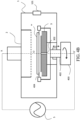
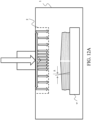
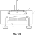
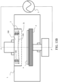
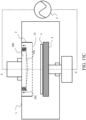
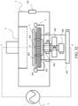
- the present invention also provides a thin film deposition device, including: a processing chamber configured for thin film deposition; a gas supply assembly arranged on the top wall of the processing chamber for supplying process gas to the processing chamber; a heating tray arranged below the gas supply assembly for bearing and heating the substrate; a radio frequency source for providing radio frequency power to activate the process gas in the processing chamber to dissociate into plasma and deposit a thin film on the substrate; a rotating mechanism for controlling the synchronous rotation of the substrate and the heating tray, the rotation shaft of the rotating mechanism being perpendicular to the substrate and passing through the substrate; wherein the rotating mechanism is connected to the heating tray and configured for driving the heating tray to rotate around the center shaft of the substrate as the shaft of rotation to rotate the substrate synchronously.
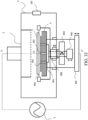
- the present invention also provides a thin film deposition device, comprising: a processing chamber configured for thin film deposition; a gas supply assembly arranged on the top wall of the processing chamber for supplying process gas to the processing chamber; a heating tray arranged below the gas supply assembly for bearing and heating a substrate; a radio frequency source for providing radio frequency power to activate the process gas in the processing chamber to dissociate into plasma and deposit a thin film on the substrate; a rotating mechanism for controlling the rotation of the heating tray, the rotation shaft of the rotating mechanism being perpendicular to the substrate and passing through the substrate; a supporting member for supporting the substrate; a lifting member connected to the supporting member and configured for driving the supporting member to rise or fall in the vertical direction to lift the substrate away from the heating tray or place the substrate on the heating tray; wherein the rotating mechanism is connected to the heating tray and configured for driving the heating tray to rotate around the center shaft of the substrate as the shaft of rotation.
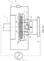
- the present invention also provides a thin film deposition device, comprising: a processing chamber configured for thin film deposition; a gas supply assembly arranged on the top wall of the processing chamber and for supplying process gas to the processing chamber; a heating tray arranged below the gas supply assembly for bearing and heating a substrate; a radio frequency source for providing radio frequency power to activate the process gas in the processing chamber to dissociate into plasma and deposit a thin film on the substrate; a rotating mechanism for controlling the rotation of the substrate, the rotation shaft of the rotating mechanism being perpendicular to the substrate and passing through the substrate; a lifting member connected to the heating tray and configured for driving the heating tray to rise or fall in vertical direction; a supporting member for supporting the substrate; wherein the rotating mechanism drives the supporting member to rotate synchronously with the substrate.
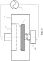
- the present invention also provides a thin film deposition device, comprising: a processing chamber configured for thin film deposition; a gas supply assembly arranged on the top wall of the processing chamber and for supplying process gas to the processing chamber; a heating tray arranged below the gas supply assembly for bearing and heating a substrate; a radio frequency source for providing radio frequency power to activate the process gas in the processing chamber to dissociate into plasma and deposit a thin film on the substrate; a rotating mechanism connected to the heating tray for driving the heating tray to rotate around the center shaft of the substrate as the shaft of rotation to rotate the substrate synchronously; when the rotating mechanism drives the heating tray to drive the substrate to rotate synchronously, the radio frequency source is adjusted to be off.
- the present invention also provides a thin film deposition device, comprising: a processing chamber configured for thin film deposition; a gas supply assembly arranged on the top wall of the processing chamber for supplying process gas to the processing chamber; a heating tray arranged below the gas supply assembly for bearing and heating a substrate; a radio frequency source for providing radio frequency power to activate the process gas in the processing chamber to dissociate into plasma and deposit a thin film on the substrate; a supporting member for supporting the substrate; a lifting member connected to the supporting member for driving the supporting member to rise or fall in the vertical direction to lift the substrate away from the heating tray or place the substrate on the heating tray; a rotating mechanism connected to the heating tray for driving the heating tray to rotate around the center shaft of the substrate as the shaft of rotation to rotate the substrate synchronously; when the rotating mechanism drives the heating tray to drive the substrate to rotate synchronously, the radio frequency source is adjusted to be off.
- the present invention also provides a thin film deposition apparatus, comprising: a processing chamber configured for thin film deposition; a gas supply assembly arranged on the top wall of the processing chamber for supplying process gas to the processing chamber; a heating tray arranged below the gas supply assembly for bearing and heating the substrate; a radio frequency source for providing radio frequency power to activate the process gas in the processing chamber to dissociate into plasma and deposit a thin film on the substrate; a lifting member connected to the gas supply assembly for driving the gas supply assembly to rise or fall.
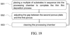
- the present invention also provides a thin film deposition device, comprising: a processing chamber configured for thin film deposition; a gas supply assembly having a first porous plate arranged on the top wall of the processing chamber for supplying process gas to the processing chamber; a heating tray arranged below the gas supply assembly for bearing and heating a substrate; a gas regulating unit arranged in the gas supply assembly having a second porous plate which is arranged opposite to the first porous plate of the gas supply assembly, the gap between the second porous plate and the first porous plate being adjustable.
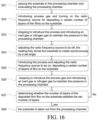
- the present invention also provides a thin film deposition method, comprising the following steps: S1, placing the substrate in the processing chamber and evacuating the processing chamber; S2, introducing process gas into the processing chamber and turning on the radio frequency source to deposit a certain number of layers of thin films on the substrate; S3, stopping to introduce the process gas and introducing non-process gas to maintain the pressure in the processing chamber; S4, keeping the radio frequency source in an on state, rotating the substrate or the heating tray or the substrate and the heating tray synchronously by a set angle; S5, introducing process gas into the processing chamber again and re-depositing a certain number of layers of thin films on the substrate; S6, stopping to introduce the process gas and introducing non-process gas to maintain the pressure in the processing chamber; S7, determining whether the number of layers of the film deposited on the substrate meets the requirements; if not, going back to step S2; if yes, executing step S8; S8, taking out the substrate from the processing chamber.
- the present invention also provides a thin film deposition method, comprising the following steps: S11, placing the substrate in the processing chamber and evacuating the processing chamber; S12, introducing the process gas into the processing chamber and turning on the radio frequency source to deposit a certain film thickness of thin film on the substrate; S13, introducing the process gas, keeping the radio frequency source in an on state, rotating the substrate or the heating tray or the substrate and the heating tray synchronously by a set angle; S14, depositing a thin film on the substrate; S15, determining whether the thickness of the deposited film on the substrate meets the requirements, if not, going back to step S12; if yes, executing step S16; S16, taking out the substrate from the processing chamber.
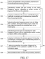
- the present invention also provides a thin film deposition method, comprising the following steps: S31, placing the substrate in the processing chamber and evacuating the processing chamber; S32, introducing process gas into the processing chamber and turning on the radio frequency source to deposit a certain number of layers of thin films on the substrate; S33, stopping to introduce the process gas and introducing non-process gas to maintain the pressure in the processing chamber; S34, adjusting the radio frequency source to be off state, lifting the substrate to rotate the heating tray at a set angle, and then placing the substrate back on the heating tray; S35, introducing process gas into the processing chamber and adjusting the radio frequency source to be on state to deposit a certain number of layers of thin films on the substrate; S36, stopping to introduce the process gas and introducing non-process gas to maintain the pressure in the processing chamber; S37, determining whether the number of layers of the deposited thin film on the substrate meets the requirements; if not, going back to step S32; if yes, executing step S38; S38, taking out the substrate from the processing chamber.
- the problem of poor uniformity of the deposited film when the substrate is deposited super multi-layers (for example, >200 layers) is solved.
- the uniformity and stability of the film deposition of the PECVD layer stack structure is realized.
- the phenomenon that the thin film deposited on the substrate deviates from the vertical direction during the subsequent etching process is avoided, thereby the stability of the performance of the semiconductor device is ensured.
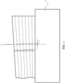
- the uniformity of the film becomes worse during the film deposition process.
- the thickness of the thin film of the layer stack structure formed on the substrate w increases with the number of layers that the first material and the second material alternately stacked on the substrate w increases.
- above problems results in a tilt of the stacked films by an angle ⁇ .
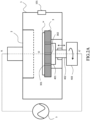
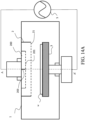
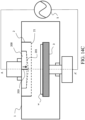
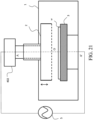
- the embodiment 1 proposes to keep the radio frequency source 5 in an on state while driving the substrate to rotate to compensate for the uneven thickness of the film deposited on the substrate w.
- the embodiment realizes the uniformity and stability of the film deposition of the PECVD layer stack structure and avoids the phenomenon that the thin film deposited on the substrate w deviates from the vertical direction during the subsequent etching process, thereby further ensuring the stability of the performance of the semiconductor device.
- the heating tray 3 is provided with a second through hole 302. Keeping the radio frequency source 5 in an on state while the substrate is rotating and introducing the non-process gas into the gap between the substrate w and the heating tray 3 through the second through hole 302 to reduce the risk of arc discharge when the substrate w is detached from the heating tray 3.
- the non-process gas is inert gas or nitrogen in an embodiment.
- the radio frequency source 5 After depositing a certain number of layers of film on the substrate w, some impurity particles are suspended in the processing chamber 1. At this time, keeping the radio frequency source 5 in an on state and filling the processing chamber 1 with a radio frequency electric field, the impurity particles are charged under the action of the internal radio frequency electric field in the processing chamber 1. The charged impurity particles remain suspended and will not fall on the surface of the substrate w to prevent the impurity particles from falling on the thin film deposited on the substrate w effectively to avoid contamination of the thin film deposited on the substrate w. Therefore, when the gap between the substrate w and the heating tray 3 is filled with non-process gas, the radio frequency source 5 is kept in an on state to reduce the risk of arc discharge on the substrate w and ensure the safety and stability of the thin film deposition process.
- Embodiment 3 provides a thin film deposition device, compared with the embodiment 1, the difference is:
- the radio frequency source 5 is adjusted to be off and purify the processing chamber 1.
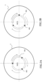
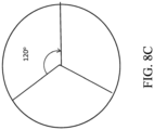
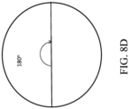
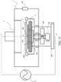
- the heating tray 3 drives the substrate w to rotate synchronously with the shaft AA' passing through the center of the substrate w as the rotation shaft including: after the heated tray 3 is rotated around the rotation shaft AA' in the forward direction by a set angle, it will be rotated around the rotation shaft AA' in the reverse direction.
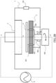
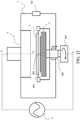
- the thin film deposition device also includes: a supporting member configured to support the substrate w, wherein the supporting member is a supporting ring 404 arranged at the bottom of the edge of the substrate w; a lifting member 402 connected to the supporting ring 404 and configured to drive the supporting ring 404 to rise or fall in a vertical direction to lift the substrate w away from the heating tray 3 or place the substrate w on the heating tray 3 .
- the rotating mechanism 403 is connected to the heating tray 3 for driving the heating tray 3 to rotate around the shaft AA' passing through the center of the substrate w.
- the processing chamber 1 is connected to an air pump for extracting exhaust gas during the deposition process of the processing chamber 1.
- the extraction of the exhaust gas by the air pump may easily leads to the gas flow at the outer periphery of the gas supply assembly 2 being greater than the gas flow at the central position of the gas supply assembly 2 that resulting in the thickness of the thin film deposited on the substrate w at the central position is smaller than the thickness of the thin film at the outer periphery. It also results in incline at a certain angle ⁇ of the film stacked on the surface of the substrate w and uneven thickness of the deposited film on the substrate w, which leads to the defect that the etched through hole deviates from the vertical direction during the subsequent etching process.
- the thin film deposition device also includes a controller, which is respectively connected to the gas supply assembly 2, the heating tray 3, and the gas regulating unit 200. The controller is configured to control the gas supply assembly 2, the heating tray 3, and the gas regulating unit 200 to work.
- the side wall 202 of the gas regulating unit 200 is a bellow, which can be stretched vertically downwards or shrunk upwards.
- the second porous plate 201 at the bottom of the gas regulating unit 200 is bent or arc-shaped to adjust the gap between the second porous plate 201 and the first porous plate 21, so that the process gas in the gas supply assembly 2 can be fully mixed. It also improves the defect that the uneven deposition of the film on the surface of the substrate w caused by the uneven distribution of the plasma.
- the embodiment provides a thin film deposition device, compared with the embodiment 12, the difference is:
- the gas regulating unit 200 includes a telescopic rod 203, and the telescopic rod 203 is connected to the second porous plate 201.
- the telescopic rod 203 can be stretched or shrunk in the vertical direction, so that the second porous plate 201 is bent or arc-shaped to adjust the gap between the second porous plate 201 and the first porous plate 21.
- the process gas in the gas supply assembly 2 can be fully mixed to improving the defects of non-uniform film deposition on the surface caused by uneven distribution of the plasma in the processing chamber 1.
- the telescopic rod 203 is arranged at the center of the gas regulating unit 200 and connected to the center of the second perforated plate 201.
- the rotation shaft AA' of the rotation of the substrate w or the rotation of the heating tray 3 or the synchronous rotation of the substrate w and the heating tray 3 is perpendicular to and passing through the center O of the substrate w.
- the thin film deposition method further includes: after each material is deposited on the surface of the substrate w, the waste gas in the processing chamber 1 needs to be pumped away, and then subsequent process steps are performed.
- the embodiment 19 provides a thin film deposition method, which is realized based on the thin film deposition device in the above-mentioned embodiment 8 and embodiment 11.
- the thin film deposited on the substrate w includes the first material and the second material deposited alternately.
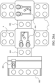
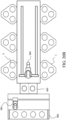
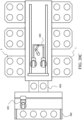
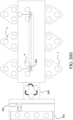
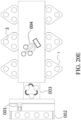
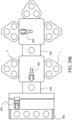
- the multiple processing chambers 1 of the thin film deposition device there are multiple processing chambers 1 of the thin film deposition device, and the multiple processing chambers 1 are symmetrically arranged on both sides of the process manipulator 004.
- the heating tray 3 and the substrate w move synchronously under the driving of the first lifting member 402 and the second lifting member 405 to adjust the distance between the gas supply assembly 2 and the substrate w.
- the heating tray 3 is provided with a groove corresponding to the position of the ejector pin 401, and the top of the ejector pin 401 is provided with a convex portion.
- the heating tray 3 moves upward, the convex portion of the ejector pin 401 is accommodated in the groove.
- the heating tray 3 continues to move upward and take the ejector pin 401 to move upward together. After the ejector pin 401 moves upward, the ejector pin 401 is separated from the base 6, and the ejector pin 401 is in a suspended state.
- the heights of the three sets of ejector pins are stepped, and the received substrate w is correspondingly configured in a stepped shape.
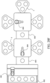
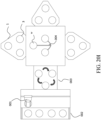
- Three heating trays 3 are arranged in a triangular structure.
- the structure of the process manipulator 004 matches the triangular structure formed by the three heating trays 3 in the processing chamber 1.
- the process manipulator 004 respectively places three substrates w according to the heights of the three sets of ejector pins from high to low. Specifically, such as FIG.
Landscapes
- Chemical & Material Sciences (AREA)
- Engineering & Computer Science (AREA)
- General Chemical & Material Sciences (AREA)
- Chemical Kinetics & Catalysis (AREA)
- Materials Engineering (AREA)
- Mechanical Engineering (AREA)
- Metallurgy (AREA)
- Organic Chemistry (AREA)
- Physics & Mathematics (AREA)
- Plasma & Fusion (AREA)
- Inorganic Chemistry (AREA)
- Chemical Vapour Deposition (AREA)
Applications Claiming Priority (2)
| Application Number | Priority Date | Filing Date | Title |
|---|---|---|---|
| CN202111027306 | 2021-09-02 | ||
| PCT/CN2022/116482 WO2023030439A1 (zh) | 2021-09-02 | 2022-09-01 | 薄膜沉积装置、薄膜沉积方法及薄膜沉积设备 |
Publications (2)
| Publication Number | Publication Date |
|---|---|
| EP4397784A1 true EP4397784A1 (de) | 2024-07-10 |
| EP4397784A4 EP4397784A4 (de) | 2026-03-18 |
Family
ID=85293008
Family Applications (1)
| Application Number | Title | Priority Date | Filing Date |
|---|---|---|---|
| EP22863574.4A Pending EP4397784A4 (de) | 2021-09-02 | 2022-09-01 | Dünnschichtabscheidungsvorrichtung, dünnschichtabscheidungsverfahren und dünnschichtabscheidungsvorrichtung |
Country Status (7)
| Country | Link |
|---|---|
| US (1) | US20240368766A1 (de) |
| EP (1) | EP4397784A4 (de) |
| JP (1) | JP2024530804A (de) |
| KR (1) | KR20240049393A (de) |
| CN (1) | CN115725953A (de) |
| TW (2) | TW202311552A (de) |
| WO (1) | WO2023030439A1 (de) |
Families Citing this family (5)
| Publication number | Priority date | Publication date | Assignee | Title |
|---|---|---|---|---|
| CN119433514B (zh) * | 2023-08-04 | 2025-12-30 | 盛美半导体设备(上海)股份有限公司 | 薄膜沉积装置及薄膜沉积方法 |
| CN119506846B (zh) * | 2023-08-23 | 2025-12-30 | 盛美半导体设备(上海)股份有限公司 | 硅片托举环、薄膜沉积设备及薄膜沉积方法 |
| CN120174351A (zh) * | 2023-12-18 | 2025-06-20 | 盛美半导体设备(上海)股份有限公司 | 薄膜沉积装置及薄膜沉积方法 |
| CN120425319A (zh) * | 2024-02-05 | 2025-08-05 | 盛美半导体设备(上海)股份有限公司 | 一种气流调节结构及气流调节方法 |
| CN119640237B (zh) * | 2024-12-10 | 2025-11-11 | 拓荆科技(上海)有限公司 | 一种降低部件氧化的加热盘装置及其薄膜沉积设备 |
Family Cites Families (21)
| Publication number | Priority date | Publication date | Assignee | Title |
|---|---|---|---|---|
| US4987856A (en) * | 1989-05-22 | 1991-01-29 | Advanced Semiconductor Materials America, Inc. | High throughput multi station processor for multiple single wafers |
| US5665640A (en) * | 1994-06-03 | 1997-09-09 | Sony Corporation | Method for producing titanium-containing thin films by low temperature plasma-enhanced chemical vapor deposition using a rotating susceptor reactor |
| JP4203206B2 (ja) * | 2000-03-24 | 2008-12-24 | 株式会社日立国際電気 | 基板処理装置 |
| JP2004277864A (ja) * | 2003-03-18 | 2004-10-07 | Toshiba Corp | 成膜方法及び成膜装置 |
| US8440259B2 (en) * | 2007-09-05 | 2013-05-14 | Intermolecular, Inc. | Vapor based combinatorial processing |
| CN103348776B (zh) * | 2011-02-15 | 2017-06-09 | 应用材料公司 | 多区等离子体生成的方法和设备 |
| JP2013042061A (ja) * | 2011-08-19 | 2013-02-28 | Hitachi Kokusai Electric Inc | 基板処理装置及び半導体装置の製造方法 |
| US8920888B2 (en) * | 2012-04-04 | 2014-12-30 | Taiwan Semiconductor Manufacturing Company, Ltd. | Plasma process, film deposition method and system using rotary chuck |
| US9840777B2 (en) * | 2014-06-27 | 2017-12-12 | Applied Materials, Inc. | Apparatus for radical-based deposition of dielectric films |
| US9214333B1 (en) * | 2014-09-24 | 2015-12-15 | Lam Research Corporation | Methods and apparatuses for uniform reduction of the in-feature wet etch rate of a silicon nitride film formed by ALD |
| US9490116B2 (en) * | 2015-01-09 | 2016-11-08 | Applied Materials, Inc. | Gate stack materials for semiconductor applications for lithographic overlay improvement |
| CN106548916B (zh) * | 2015-09-16 | 2018-11-06 | 北京北方华创微电子装备有限公司 | 工艺腔室、半导体加工设备及去气和预清洗的方法 |
| JP6918554B2 (ja) * | 2017-04-06 | 2021-08-11 | 東京エレクトロン株式会社 | 可動体構造及び成膜装置 |
| US10851457B2 (en) * | 2017-08-31 | 2020-12-01 | Lam Research Corporation | PECVD deposition system for deposition on selective side of the substrate |
| CN109423630A (zh) * | 2017-09-04 | 2019-03-05 | 台湾积体电路制造股份有限公司 | 升举装置、化学气相沉积装置及方法 |
| US10714372B2 (en) * | 2017-09-20 | 2020-07-14 | Applied Materials, Inc. | System for coupling a voltage to portions of a substrate |
| US11276569B2 (en) * | 2018-07-31 | 2022-03-15 | Applied Materials, Inc. | On stack overlay improvement for 3D NAND |
| US11901162B2 (en) * | 2019-01-07 | 2024-02-13 | Ulvac, Inc. | Vacuum processing apparatus and method of cleaning vacuum processing apparatus |
| WO2021091786A1 (en) * | 2019-11-04 | 2021-05-14 | Applied Materials, Inc. | Systems and methods for substrate support temperature control |
| CN111364026B (zh) * | 2020-05-27 | 2020-08-14 | 上海陛通半导体能源科技股份有限公司 | 往复式旋转cvd设备及应用方法 |
| US11887811B2 (en) * | 2020-09-08 | 2024-01-30 | Applied Materials, Inc. | Semiconductor processing chambers for deposition and etch |
-
2021
- 2021-12-07 TW TW110145749A patent/TW202311552A/zh unknown
-
2022
- 2022-09-01 WO PCT/CN2022/116482 patent/WO2023030439A1/zh not_active Ceased
- 2022-09-01 JP JP2024514471A patent/JP2024530804A/ja active Pending
- 2022-09-01 EP EP22863574.4A patent/EP4397784A4/de active Pending
- 2022-09-01 CN CN202211066276.0A patent/CN115725953A/zh active Pending
- 2022-09-01 US US18/689,038 patent/US20240368766A1/en active Pending
- 2022-09-01 KR KR1020247010924A patent/KR20240049393A/ko active Pending
- 2022-09-02 TW TW111133456A patent/TW202311560A/zh unknown
Also Published As
| Publication number | Publication date |
|---|---|
| US20240368766A1 (en) | 2024-11-07 |
| TW202311560A (zh) | 2023-03-16 |
| KR20240049393A (ko) | 2024-04-16 |
| CN115725953A (zh) | 2023-03-03 |
| EP4397784A4 (de) | 2026-03-18 |
| JP2024530804A (ja) | 2024-08-23 |
| WO2023030439A1 (zh) | 2023-03-09 |
| TW202311552A (zh) | 2023-03-16 |
Similar Documents
| Publication | Publication Date | Title |
|---|---|---|
| EP4397784A1 (de) | Dünnschichtabscheidungsvorrichtung, dünnschichtabscheidungsverfahren und dünnschichtabscheidungsvorrichtung | |
| WO2023028963A1 (zh) | 薄膜沉积装置及薄膜沉积方法及薄膜沉积设备 | |
| US6746195B2 (en) | Semiconductor transfer and manufacturing apparatus | |
| CN101136349B (zh) | 衬底传送装置、衬底处理装置和传送衬底的方法 | |
| KR100269097B1 (ko) | 기판처리장치 | |
| KR101676066B1 (ko) | 도포 처리 장치, 도포 현상 처리 시스템 및 도포 처리 방법 및 그 도포 처리 방법을 실행시키기 위한 프로그램을 기록한 기록 매체 | |
| US20070245949A1 (en) | Substrate carrying and processing apparatus | |
| JP2000306978A (ja) | 基板処理装置、基板搬送装置、および基板処理方法 | |
| JP2012004536A (ja) | 基板処理装置及び基板処理方法 | |
| CN1909182A (zh) | 半导体工艺处理系统及其处理方法 | |
| US10854497B2 (en) | Apparatus and method of selective turning over a row of substrates in an array of substrates in a processing system | |
| CN1729552A (zh) | 大面积基板处理系统 | |
| JP2001093899A (ja) | 絶縁膜形成方法及び絶縁膜形成装置 | |
| WO1999052143A1 (fr) | Mecanisme d'alignement et dispositif de traitement de semi-conducteurs utilisant ce mecanisme | |
| TW202507059A (zh) | 薄膜沉積裝置及薄膜沉積方法 | |
| CN102194665B (zh) | 处理室、半导体制造设备及使用其的基板处理方法 | |
| KR100873967B1 (ko) | 완충메카니즘을 갖는 반도체 제조장치 및 반도체 웨이퍼의완충방법 | |
| JP2018056340A (ja) | 基板配列装置および基板配列方法 | |
| KR100317462B1 (ko) | 기판 처리 장치 | |
| US20060156982A1 (en) | Apparatus for fabricating semiconductor device | |
| CN113005423A (zh) | 处理体收纳装置及包含处理体收纳装置的成膜装置 | |
| CN223828417U (zh) | 一种多片晶圆同时注入的离子注入系统 | |
| CN120366750A (zh) | 基片处理装置 | |
| JPH1150252A (ja) | 真空処理装置 | |
| CN119177435A (zh) | 在线换位的化学气相沉积设备及其加工方法 |
Legal Events
| Date | Code | Title | Description |
|---|---|---|---|
| STAA | Information on the status of an ep patent application or granted ep patent |
Free format text: STATUS: THE INTERNATIONAL PUBLICATION HAS BEEN MADE |
|
| PUAI | Public reference made under article 153(3) epc to a published international application that has entered the european phase |
Free format text: ORIGINAL CODE: 0009012 |
|
| STAA | Information on the status of an ep patent application or granted ep patent |
Free format text: STATUS: REQUEST FOR EXAMINATION WAS MADE |
|
| 17P | Request for examination filed |
Effective date: 20240325 |
|
| AK | Designated contracting states |
Kind code of ref document: A1 Designated state(s): AL AT BE BG CH CY CZ DE DK EE ES FI FR GB GR HR HU IE IS IT LI LT LU LV MC MK MT NL NO PL PT RO RS SE SI SK SM TR |
|
| DAV | Request for validation of the european patent (deleted) | ||
| DAX | Request for extension of the european patent (deleted) | ||
| A4 | Supplementary search report drawn up and despatched |
Effective date: 20260212 |
|
| RIC1 | Information provided on ipc code assigned before grant |
Ipc: C23C 16/458 20060101AFI20260206BHEP Ipc: C23C 16/455 20060101ALI20260206BHEP Ipc: C23C 16/50 20060101ALI20260206BHEP Ipc: C23C 16/52 20060101ALI20260206BHEP Ipc: C23C 16/46 20060101ALI20260206BHEP Ipc: C23C 16/505 20060101ALI20260206BHEP Ipc: C23C 16/02 20060101ALI20260206BHEP |