EP4397905A1 - Schaltungsvorrichtung und beleuchtungsvorrichtung - Google Patents
Schaltungsvorrichtung und beleuchtungsvorrichtung Download PDFInfo
- Publication number
- EP4397905A1 EP4397905A1 EP22864100.7A EP22864100A EP4397905A1 EP 4397905 A1 EP4397905 A1 EP 4397905A1 EP 22864100 A EP22864100 A EP 22864100A EP 4397905 A1 EP4397905 A1 EP 4397905A1
- Authority
- EP
- European Patent Office
- Prior art keywords
- circuit
- circuit device
- power
- electrified track
- power conversion
- Prior art date
- Legal status (The legal status is an assumption and is not a legal conclusion. Google has not performed a legal analysis and makes no representation as to the accuracy of the status listed.)
- Granted
Links
Images

Classifications
-
- F—MECHANICAL ENGINEERING; LIGHTING; HEATING; WEAPONS; BLASTING
- F21—LIGHTING
- F21S—NON-PORTABLE LIGHTING DEVICES; SYSTEMS THEREOF; VEHICLE LIGHTING DEVICES SPECIALLY ADAPTED FOR VEHICLE EXTERIORS
- F21S2/00—Systems of lighting devices, not provided for in main groups F21S4/00 - F21S10/00 or F21S19/00, e.g. of modular construction
-
- F—MECHANICAL ENGINEERING; LIGHTING; HEATING; WEAPONS; BLASTING
- F21—LIGHTING
- F21V—FUNCTIONAL FEATURES OR DETAILS OF LIGHTING DEVICES OR SYSTEMS THEREOF; STRUCTURAL COMBINATIONS OF LIGHTING DEVICES WITH OTHER ARTICLES, NOT OTHERWISE PROVIDED FOR
- F21V21/00—Supporting, suspending, or attaching arrangements for lighting devices; Hand grips
- F21V21/34—Supporting elements displaceable along a guiding element
- F21V21/35—Supporting elements displaceable along a guiding element with direct electrical contact between the supporting element and electric conductors running along the guiding element
-
- F—MECHANICAL ENGINEERING; LIGHTING; HEATING; WEAPONS; BLASTING
- F21—LIGHTING
- F21V—FUNCTIONAL FEATURES OR DETAILS OF LIGHTING DEVICES OR SYSTEMS THEREOF; STRUCTURAL COMBINATIONS OF LIGHTING DEVICES WITH OTHER ARTICLES, NOT OTHERWISE PROVIDED FOR
- F21V23/00—Arrangement of electric circuit elements in or on lighting devices
-
- H—ELECTRICITY
- H05—ELECTRIC TECHNIQUES NOT OTHERWISE PROVIDED FOR
- H05B—ELECTRIC HEATING; ELECTRIC LIGHT SOURCES NOT OTHERWISE PROVIDED FOR; CIRCUIT ARRANGEMENTS FOR ELECTRIC LIGHT SOURCES, IN GENERAL
- H05B45/00—Circuit arrangements for operating light-emitting diodes [LED]
- H05B45/30—Driver circuits
- H05B45/37—Converter circuits
-
- H—ELECTRICITY
- H05—ELECTRIC TECHNIQUES NOT OTHERWISE PROVIDED FOR
- H05B—ELECTRIC HEATING; ELECTRIC LIGHT SOURCES NOT OTHERWISE PROVIDED FOR; CIRCUIT ARRANGEMENTS FOR ELECTRIC LIGHT SOURCES, IN GENERAL
- H05B47/00—Circuit arrangements for operating light sources in general, i.e. where the type of light source is not relevant
- H05B47/10—Controlling the light source
- H05B47/175—Controlling the light source by remote control
- H05B47/19—Controlling the light source by remote control via wireless transmission
-
- F—MECHANICAL ENGINEERING; LIGHTING; HEATING; WEAPONS; BLASTING
- F21—LIGHTING
- F21Y—INDEXING SCHEME ASSOCIATED WITH SUBCLASSES F21K, F21L, F21S and F21V, RELATING TO THE FORM OR THE KIND OF THE LIGHT SOURCES OR OF THE COLOUR OF THE LIGHT EMITTED
- F21Y2115/00—Light-generating elements of semiconductor light sources
- F21Y2115/10—Light-emitting diodes [LED]
-
- F—MECHANICAL ENGINEERING; LIGHTING; HEATING; WEAPONS; BLASTING
- F21—LIGHTING
- F21Y—INDEXING SCHEME ASSOCIATED WITH SUBCLASSES F21K, F21L, F21S and F21V, RELATING TO THE FORM OR THE KIND OF THE LIGHT SOURCES OR OF THE COLOUR OF THE LIGHT EMITTED
- F21Y2115/00—Light-generating elements of semiconductor light sources
- F21Y2115/10—Light-emitting diodes [LED]
- F21Y2115/15—Organic light-emitting diodes [OLED]
-
- H—ELECTRICITY
- H05—ELECTRIC TECHNIQUES NOT OTHERWISE PROVIDED FOR
- H05B—ELECTRIC HEATING; ELECTRIC LIGHT SOURCES NOT OTHERWISE PROVIDED FOR; CIRCUIT ARRANGEMENTS FOR ELECTRIC LIGHT SOURCES, IN GENERAL
- H05B45/00—Circuit arrangements for operating light-emitting diodes [LED]
- H05B45/30—Driver circuits
- H05B45/37—Converter circuits
- H05B45/3725—Switched mode power supply [SMPS]
- H05B45/375—Switched mode power supply [SMPS] using buck topology
-
- H—ELECTRICITY
- H05—ELECTRIC TECHNIQUES NOT OTHERWISE PROVIDED FOR
- H05B—ELECTRIC HEATING; ELECTRIC LIGHT SOURCES NOT OTHERWISE PROVIDED FOR; CIRCUIT ARRANGEMENTS FOR ELECTRIC LIGHT SOURCES, IN GENERAL
- H05B45/00—Circuit arrangements for operating light-emitting diodes [LED]
- H05B45/30—Driver circuits
- H05B45/37—Converter circuits
- H05B45/3725—Switched mode power supply [SMPS]
- H05B45/39—Circuits containing inverter bridges
Definitions
- the present invention provides a circuit device that is less likely to become visual noise for users, and a lighting device including the circuit device.
- a lighting device includes: the circuit device described above; and a light source device that illuminates surroundings of the circuit device by emitting light using power obtained by conversion by the power conversion circuit.
- the present invention enables implementation of the circuit device that is less likely to become visual noise for users, and the lighting device including the circuit device.
- a Z-axis direction is described as a height direction of a lighting device.
- a Z-axis positive (+) side may be described as an upper side (upside), and a Z-axis negative (-) side may be described as a lower side (downside).
- An X-axis direction and a Y-axis direction are directions orthogonal to each other in a plane perpendicular to the Z-axis direction.
- planar view means viewing from the Z-axis direction.
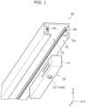
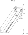
- FIGS. 1 to 3 each show a perspective view illustrating an appearance of the circuit device according to Embodiment 1.
- FIG. 1 is a diagram illustrating a state in which locking part 12b and a pair of electrodes 12c included in circuit device 10 are housed inside enclosure 11.
- FIG. 2 is a diagram illustrating a state in which locking part 12b and the pair of electrodes 12c, which are included in circuit device 10, protrude outward from enclosure 11.
- FIG. 3 is a diagram illustrating a state in which circuit device 10 is attached to electrified track 50.
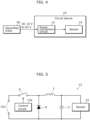
- FIG. 4 is a block diagram illustrating a functional configuration of circuit device 10.
- Enclosure 11 houses power conversion circuit 13 and sensor 14.
- Enclosure 11 is, for example, of a rectangular parallelepiped shape that is elongated along a longitudinal direction of electrified track 50.
- Enclosure 11 is formed, for example, by a resin material, but may also be formed by a metal material with a surface subjected to insulating treatment.
- enclosure 11 is entirely located within groove 51 included in electrified track 50. More specifically, in the state in which circuit device 10 is attached to electrified track 50, no part of enclosure 11 protrudes below lower surface 52 of electrified track 50. This prevents enclosure 11 from becoming visual noise.
- a height (length in the Z-axis direction) of enclosure 11 is, for example, 15 mm or less
- a width (length in the X-axis direction) of enclosure 11 is, for example, 14 mm or less
- a length (length in the Y-axis direction) of enclosure 11 is, for example, 200 mm or less.
- Attachment mechanism 12 is a mechanism for attaching circuit device 10 to electrified track 50.
- Attachment mechanism 12 includes knob 12a, locking part 12b, and the pair of electrodes 12c (in FIG. 2 , only one of the pair of electrodes 12c is shown).
- Knob 12a and locking part 12b are formed, for example, by a resin material, and the pair of electrodes 12c are formed, for example, by a metal material such as copper.
- attachment mechanism 12 the electrical connection and disconnection of the pair of electrodes 12c to and from power supply terminals 54 (electrified track 50) are linked with attachment mechanism 12, but do not necessarily need to be linked with attachment mechanism 12.
- another knob may be provided to switch between the electrical connection of the pair of electrodes 12c to power supply terminals 54 (electrified track 50) and the electrical disconnection of the pair of electrodes 12c from power supply terminals 54.
- Power conversion circuit 13 is a direct current (DC)-DC converter that converts DC power supplied from electrified track 50 into DC power with a different voltage.
- power conversion circuit 13 is a non-isolated DC-DC converter that converts DC power supplied from electrified track 50 with a voltage of 10 V or more and 63 V or less into DC power with a voltage suitable for operations of sensor 14.
- FIG. 5 is a diagram illustrating an example of a circuit configuration of power conversion circuit 13.
- FIG. 5 shows an example of the circuit configuration, and any existing circuit configuration may be used for power conversion circuit 13.
- Power conversion circuit 13 is implemented by mounting circuit components on a board. As shown in FIG. 5 , the circuit components of power conversion circuit 13 include, for example, control circuit 13a, switching element S, diode D, inductor L, and smoothing capacitor C. In FIG. 5 , the pair of electrodes 12c and sensor 14 are also illustrated together.
- Control circuit 13a is a control circuit that controls on and off of switching element S.
- control circuit 13a is a packaged integrated circuit (IC).
- Control circuit 13a switches a DC voltage applied between the pair of electrodes 12c by controlling the on and off of switching element S.
- a high-frequency voltage is outputted to inductor L.
- Switching element S is, for example, a field effect transistor (FET), but may also be a bipolar transistor.
- a switching element made of gallium nitride (GaN) semiconductor may be employed as switching element S as necessary.
- Diode D is a reflux diode that regenerates current when switching element S is off. Smoothing capacitor C smooths the current outputted from inductor L. Power smoothed by smoothing capacitor C is outputted to sensor 14.
- power conversion circuit 13 to be compactly formed, and allows power conversion circuit 13 to be entirely located inside electrified track 50.
- Power conversion circuit 13 being located inside electrified track 50 means that power conversion circuit 13 is at least partially located in groove 51.
- the expression that power conversion circuit 13 is located inside electrified track 50 includes a case where entire (whole) power conversion circuit 13 is located in groove 51 and a lower end of power conversion circuit 13 (the board on which the circuit components are mounted) does not protrude below lower surface 52 of electrified track 50.
- the expression that power conversion circuit 13 is located inside electrified track 50 also includes a case where all of the circuit components substantially constituting power conversion circuit 13 are located in groove 51 and do not protrude below lower surface 52 of electrified track 50. Even if sensor 14 or a wireless communicator, for example, is mounted on the same board as power conversion circuit 13, these components are not included in the circuit components substantially constituting power conversion circuit 13, because these components do not contribute to substantial power conversion.
- the expression that power conversion circuit 13 is located inside electrified track 50 also includes a case where only part of power conversion circuit 13 is located in groove 51.
- the expression that power conversion circuit 13 is located in groove 51 includes a case where, for example, 80% or more of a volume of power conversion circuit 13 (the board on which the circuit components are mounted) is located in groove 51.
- the expression that power conversion circuit 13 is located in groove 51 also includes a case where a half or more than half of the circuit components (e.g., control circuit 13a, switching element S, diode D, inductor L, and smoothing capacitor C) of power conversion circuit 13 are located in groove 51.
- An arrangement of power conversion circuit 13 in enclosure 11 is not limited to any particular arrangement.
- Power conversion circuit 13 may be arranged in enclosure 11 such that a main surface of the board is along a Y-Z plane, or may be arranged in enclosure 11 such that the main surface of the board is along an X-Y plane.
- power conversion circuit 13 may also be a DC-AC (alternating current) converter (inverter).
- DC-AC alternating current converter
- a load included in enclosure 11 is not sensor 14 but a motor, for example, a DC-AC converter is employed as power conversion circuit 13.
- Any existing circuit configuration may be employed as a circuit configuration of the DC-AC converter.
- Sensor 14 performs sensing using power obtained by conversion by power conversion circuit 13.
- Sensor 14 is an environmental sensor that measures an environment surrounding circuit device 10, such as a temperature sensor, a humidity sensor, a carbon dioxide concentration sensor, or an electric field sensor, for example.
- Sensor 14 is mounted on the board of power conversion circuit 13, for example, but may also be mounted on a board different from the board of power conversion circuit 13. If circuit device 10 includes a wireless communication circuit, measured values of sensor 14 are transmitted to an external device by the wireless communication circuit. If circuit device 10 includes a display, the measured values of sensor 14 may be displayed on the display.
- circuit device 10 is a circuit device to be attached to electrified track 50.
- Circuit device 10 includes: attachment mechanism 12 for attaching circuit device 10 to electrified track 50; and power conversion circuit 13 that converts DC power supplied from electrified track 50. In a state in which circuit device 10 is attached to electrified track 50, power conversion circuit 13 is at least partially located inside electrified track 50.
- Circuit device 10 described above can be said to be a circuit device that is less likely to become visual noise for users because a portion of circuit device 10 protruding from electrified track 50 is reduced.
- circuit device 10 further includes electrode 12c to be electrically connected to electrified track 50 in order for power conversion circuit 13 to be supplied with the DC power. Electrical connection of electrode 12c to electrified track 50 and electrical disconnection of electrode 12c from electrified track 50 are linked with attachment mechanism 12.
- Circuit device 10 described above can be electrically connected to electrified track 50 in a manner linked with the attachment.
- power conversion circuit 13 includes switching element S, and switching element S is made of gallium nitride semiconductor.
- Circuit device 10 described above can achieve increased output and miniaturization of power conversion circuit 13.
- a rated voltage of circuit device 10 is at most 63 V.
- Circuit device 10 described above can achieve miniaturization of power conversion circuit 13 because the insulation distance required for power conversion circuit 13 to maintain is relatively short.
- circuit device 10 further includes sensor 14 that performs sensing using power obtained by conversion by power conversion circuit 13.
- Circuit device 10 described above can be used for sensing.
- Circuit device 10 described above can be said to be a circuit device that is less likely to become visual noise for users because a portion of circuit device 10 protruding from electrified track 50 can be significantly reduced.
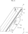
- FIG. 6 is a perspective view illustrating an appearance of the circuit device according to Embodiment 2.
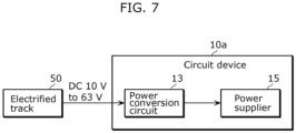
- FIG. 7 is a block diagram illustrating a functional configuration of the circuit device according to Embodiment 2.
- Embodiment 2 described below explanations will focus on differences from Embodiment 1, and explanations of previously described matters will be omitted as appropriate.
- circuit device 10a As shown in FIGS. 6 and 7 , circuit device 10a according to Embodiment 2 is attached to electrified track 50 and operates by receiving DC power from electrified track 50.
- Circuit device 10a includes enclosure 11, attachment mechanism 12, power conversion circuit 13, and power supplier 15.
- Circuit device 10a may further include sensor 14. Since enclosure 11, attachment mechanism 12, and power conversion circuit 13 have the same configurations as those in circuit device 10, detailed description of those components will be omitted.
- Power supplier 15 is a terminal structure to which a different device is structurally and electrically connected for supplying power obtained by conversion by power conversion circuit 13 to the different device.
- Single power supplier 15 is provided, for example, on a lower surface of enclosure 11, but two or more power suppliers 15 may be provided instead.
- Power supplier 15 may be provided not on the lower surface of enclosure 11, but on a tip of a cable drawn from enclosure 11.
- Power supplier 15 is implemented, for example, by a universal serial bus (USB) connector.
- USB universal serial bus
- Examples of such a USB connector include a variety of connectors such as USB Type-A, USB Type-B, USB Type-C, Mini USB Type-B, micro USB Type-B, and Lightning.
- power conversion circuit 13 converts the DC power supplied from electrified track 50 into DC power of 5 V and outputs the DC power with a voltage of 5 V to power supplier 15.
- power supplier 15 may be implemented by a USB connector.
- power supplier 15 may be implemented by an RJ-45 connector (a connector to which what is called a LAN (local area network) cable is connected) compliant with the Ethernet (registered trademark) standard.
- power supplier 15 may be implemented by an AC outlet.
- power conversion circuit 13 is a DC-AC converter (inverter) that converts the DC power supplied from electrified track 50 into AC power.
- circuit device 10a When circuit device 10a includes two or more power suppliers 15, such two or more power suppliers 15 may all have the same type of terminal structure, or may include different types of terminal structures (e.g., a USB connector and an AC outlet).
- two or more power suppliers 15 may all have the same type of terminal structure, or may include different types of terminal structures (e.g., a USB connector and an AC outlet).
- circuit device 10a is a circuit device to be attached to electrified track 50, including: attachment mechanism 12 for attaching circuit device 10a to electrified track 50; power conversion circuit 13 that converts the DC power supplied from electrified track 50; and power supplier 15 to which a different device is connected for supplying the power obtained by the conversion by power conversion circuit 13 to the different device.
- power conversion circuit 13 is at least partially located inside electrified track 50.
- Circuit device 10a described above can be said to be a power conversion device (a device that supplies the converted power to other devices) that is less likely to become visual noise for users because a portion of circuit device 10a protruding from electrified track 50 is reduced.
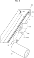
- FIG. 8 is a perspective view illustrating an appearance of the lighting device according to Embodiment 3.
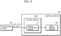
- FIG. 9 is a block diagram illustrating a functional configuration of the lighting device according to Embodiment 3.
- Embodiment 3 described below explanations will focus on differences from Embodiment 1 and Embodiment 2, and explanations of previously described matters will be omitted as appropriate.
- lighting device 30 is what is called a spotlight and includes circuit device 10b and light source device 20. Note that the present invention may be implemented as a lighting device other than a spotlight, such as a pendant light.
- Circuit device 10b is attached to electrified track 50 and operates by receiving DC power from electrified track 50.
- Circuit device 10b includes enclosure 11, attachment mechanism 12, and power conversion circuit 13.
- Circuit device 10b may further include at least one of sensor 14 or power supplier 15. Since enclosure 11, attachment mechanism 12, and power conversion circuit 13 have the same configurations as those in circuit device 10, detailed description of those components will be omitted.
- Light source device 20 illuminates the surroundings of circuit device 10b by emitting light using power obtained by conversion by power conversion circuit 13.
- Light source device 20 is provided on a lower surface of enclosure 11.
- light source device 20 is implemented, for example, by a light emitting module that emits light using the DC power supplied by power conversion circuit 13, and a lens for diffusing or collimating the light emitted by the light emitting module.
- the light emitting module is formed, for example, by mounting LED elements on a board and emits white light.
- the light emitting module may be a chip-on-board (COB) light emitting module or a surface-mount-device (SMD) light emitting module.
- COB chip-on-board
- SMD surface-mount-device
- the light emitting module may be implemented by a light emitting element other than an LED element, such as an organic electro-luminescence (EL) element.
- EL organic electro-luminescence
- the lens is, for example, a convex lens such as a Fresnel lens.
- lighting device 30 includes circuit device 10b and light source device 20 that illuminates the surroundings of circuit device 10b by emitting light using the power obtained by the conversion by power conversion circuit 13.
- Circuit device 10b is a circuit device to be attached to electrified track 50, including attachment mechanism 12 for attaching circuit device 10b to electrified track 50 and power conversion circuit 13 that converts the DC power supplied from electrified track 50.
- power conversion circuit 13 is located inside electrified track 50.
- Lighting device 30 described above can be said to be a lighting device that is less likely to become visual noise for users because a portion of lighting device 30 protruding from electrified track 50 is reduced.
- the general or specific aspects of the present invention may be implemented using a system or a device.
- the present invention may be implemented as a system including the circuit device according to any one of the above embodiments and the electrified track.
Landscapes
- Engineering & Computer Science (AREA)
- General Engineering & Computer Science (AREA)
- Computer Networks & Wireless Communication (AREA)
- Arrangement Of Elements, Cooling, Sealing, Or The Like Of Lighting Devices (AREA)
- Dc-Dc Converters (AREA)
Applications Claiming Priority (2)
| Application Number | Priority Date | Filing Date | Title |
|---|---|---|---|
| JP2021141979 | 2021-08-31 | ||
| PCT/JP2022/028388 WO2023032512A1 (ja) | 2021-08-31 | 2022-07-21 | 回路装置、及び、照明装置 |
Publications (3)
| Publication Number | Publication Date |
|---|---|
| EP4397905A1 true EP4397905A1 (de) | 2024-07-10 |
| EP4397905A4 EP4397905A4 (de) | 2024-12-18 |
| EP4397905B1 EP4397905B1 (de) | 2026-04-15 |
Family
ID=85412143
Family Applications (1)
| Application Number | Title | Priority Date | Filing Date |
|---|---|---|---|
| EP22864100.7A Active EP4397905B1 (de) | 2021-08-31 | 2022-07-21 | Schaltungsvorrichtung und beleuchtungsvorrichtung |
Country Status (5)
| Country | Link |
|---|---|
| US (1) | US12501528B2 (de) |
| EP (1) | EP4397905B1 (de) |
| JP (1) | JP7561360B2 (de) |
| CN (1) | CN117716168A (de) |
| WO (1) | WO2023032512A1 (de) |
Families Citing this family (2)
| Publication number | Priority date | Publication date | Assignee | Title |
|---|---|---|---|---|
| KR102803268B1 (ko) * | 2023-03-28 | 2025-05-07 | 주식회사 파인엘이디 | 엘이디 조명기구 |
| CN221237777U (zh) * | 2023-11-30 | 2024-06-28 | 深圳市思坎普科技有限公司 | 快拼式线条灯 |
Family Cites Families (14)
| Publication number | Priority date | Publication date | Assignee | Title |
|---|---|---|---|---|
| JP5123840B2 (ja) * | 2008-12-22 | 2013-01-23 | パナソニック株式会社 | ダクト式照明器具 |
| CN101778514B (zh) * | 2010-02-09 | 2013-03-27 | 浙江金基电子技术有限公司 | 一种led路灯能量变换和节能控制的装置 |
| JP5236123B2 (ja) * | 2011-01-11 | 2013-07-17 | 三菱電機株式会社 | Led点灯装置 |
| JP5796167B2 (ja) * | 2011-06-07 | 2015-10-21 | パナソニックIpマネジメント株式会社 | 照明システム |
| JP5994506B2 (ja) * | 2012-09-18 | 2016-09-21 | 岩崎電気株式会社 | スイッチング電源装置及び道路灯用照明器具 |
| EP3089552B1 (de) * | 2015-04-29 | 2021-03-31 | TE Connectivity Nederland B.V. | Verteilungseinheit und -system von gleichstrom-niederspannungs-strom und system für stromnetz |
| US10349483B2 (en) * | 2015-10-30 | 2019-07-09 | Cree, Inc. | Ambient light sensor circuit |
| WO2018074475A1 (ja) * | 2016-10-17 | 2018-04-26 | アルボット株式会社 | コミュニケーションロボット及びコミュニケーションシステム |
| JP7173442B2 (ja) | 2019-01-21 | 2022-11-16 | 東芝ライテック株式会社 | 取付機構および配線ダクト取付物 |
| JP7371379B2 (ja) * | 2019-07-24 | 2023-10-31 | 三菱電機株式会社 | 点灯装置、照明器具 |
| JP7308414B2 (ja) * | 2019-10-15 | 2023-07-14 | パナソニックIpマネジメント株式会社 | 接続装置、吊り具 |
| IT201900021600A1 (it) * | 2019-11-19 | 2021-05-19 | C Led Srl | Led driver per binari illuminotecnici a bassa tensione |
| IT202000002968A1 (it) * | 2020-02-14 | 2021-08-14 | C Led S R L | Lampada a binario a bassa tensione con modulo led con elettronica integrata |
| US11287122B1 (en) * | 2021-01-15 | 2022-03-29 | Diem Gmbh | Light assembly connector for insertion into both straight and curved lighting tracks |
-
2022
- 2022-07-21 CN CN202280050115.4A patent/CN117716168A/zh active Pending
- 2022-07-21 US US18/291,864 patent/US12501528B2/en active Active
- 2022-07-21 JP JP2023545152A patent/JP7561360B2/ja active Active
- 2022-07-21 EP EP22864100.7A patent/EP4397905B1/de active Active
- 2022-07-21 WO PCT/JP2022/028388 patent/WO2023032512A1/ja not_active Ceased
Also Published As
| Publication number | Publication date |
|---|---|
| EP4397905B1 (de) | 2026-04-15 |
| US20240260155A1 (en) | 2024-08-01 |
| JPWO2023032512A1 (de) | 2023-03-09 |
| JP7561360B2 (ja) | 2024-10-04 |
| WO2023032512A1 (ja) | 2023-03-09 |
| US12501528B2 (en) | 2025-12-16 |
| EP4397905A4 (de) | 2024-12-18 |
| CN117716168A (zh) | 2024-03-15 |
Similar Documents
| Publication | Publication Date | Title |
|---|---|---|
| US9366418B2 (en) | Method, apparatus and system for connecting a light emitting diode light fixture to a mains power conductor | |
| US9615414B2 (en) | Power supply device and illumination device | |
| EP4397905A1 (de) | Schaltungsvorrichtung und beleuchtungsvorrichtung | |
| US20130082595A1 (en) | Lighting apparatus | |
| US8773034B2 (en) | Power supply system for electronic loads | |
| US20160380550A1 (en) | Power Supply of transformer and light string therewith | |
| JP2010114009A (ja) | 電力供給装置、照明装置及び電力供給システム | |
| JP6655806B2 (ja) | 電源装置及びそれを用いた照明装置 | |
| CN206694853U (zh) | 光源单元和具有光源单元的照明器具 | |
| CN104704590A (zh) | 具有无线控制功能的连接器 | |
| JP6391003B2 (ja) | 電源装置及び照明器具 | |
| JP2017174568A (ja) | 光源ユニット及び照明器具 | |
| JP2009099627A (ja) | Led照明器具 | |
| CN207514631U (zh) | 发光装置、以及照明装置 | |
| US9512967B2 (en) | Straight type lamp | |
| CN212463565U (zh) | 灯带控制器和灯带装置 | |
| CN209495163U (zh) | 一种线性灯条 | |
| CN206817185U (zh) | 电源装置、光源单元和照明器具 | |
| JP2020080321A (ja) | 照明器具 | |
| JP2017084526A (ja) | 照明システム | |
| CN222073542U (zh) | 一种新型led驱动电源 | |
| JP2016046201A (ja) | 電源装置及び照明器具 | |
| JP7510599B2 (ja) | 照明装置 | |
| JP7121922B2 (ja) | 電源回路及び照明装置 | |
| CN205385637U (zh) | 固定式灯具及其电源驱动装置 |
Legal Events
| Date | Code | Title | Description |
|---|---|---|---|
| STAA | Information on the status of an ep patent application or granted ep patent |
Free format text: STATUS: THE INTERNATIONAL PUBLICATION HAS BEEN MADE |
|
| PUAI | Public reference made under article 153(3) epc to a published international application that has entered the european phase |
Free format text: ORIGINAL CODE: 0009012 |
|
| STAA | Information on the status of an ep patent application or granted ep patent |
Free format text: STATUS: REQUEST FOR EXAMINATION WAS MADE |
|
| 17P | Request for examination filed |
Effective date: 20240126 |
|
| AK | Designated contracting states |
Kind code of ref document: A1 Designated state(s): AL AT BE BG CH CY CZ DE DK EE ES FI FR GB GR HR HU IE IS IT LI LT LU LV MC MK MT NL NO PL PT RO RS SE SI SK SM TR |
|
| DAV | Request for validation of the european patent (deleted) | ||
| DAX | Request for extension of the european patent (deleted) | ||
| A4 | Supplementary search report drawn up and despatched |
Effective date: 20241118 |
|
| RIC1 | Information provided on ipc code assigned before grant |
Ipc: H05B 45/37 20200101ALI20241112BHEP Ipc: F21Y 115/15 20160101ALI20241112BHEP Ipc: F21Y 115/10 20160101ALI20241112BHEP Ipc: H05B 47/19 20200101ALI20241112BHEP Ipc: H05B 45/39 20200101ALI20241112BHEP Ipc: H05B 45/375 20200101ALI20241112BHEP Ipc: F21V 21/35 20060101ALI20241112BHEP Ipc: F21S 2/00 20160101ALI20241112BHEP Ipc: F21V 23/00 20150101AFI20241112BHEP |
|
| GRAP | Despatch of communication of intention to grant a patent |
Free format text: ORIGINAL CODE: EPIDOSNIGR1 |
|
| STAA | Information on the status of an ep patent application or granted ep patent |
Free format text: STATUS: GRANT OF PATENT IS INTENDED |
|
| INTG | Intention to grant announced |
Effective date: 20251218 |
|
| GRAS | Grant fee paid |
Free format text: ORIGINAL CODE: EPIDOSNIGR3 |
|
| GRAA | (expected) grant |
Free format text: ORIGINAL CODE: 0009210 |
|
| STAA | Information on the status of an ep patent application or granted ep patent |
Free format text: STATUS: THE PATENT HAS BEEN GRANTED |
|
| AK | Designated contracting states |
Kind code of ref document: B1 Designated state(s): AL AT BE BG CH CY CZ DE DK EE ES FI FR GB GR HR HU IE IS IT LI LT LU LV MC MK MT NL NO PL PT RO RS SE SI SK SM TR |
|
| REG | Reference to a national code |
Ref country code: CH Ref legal event code: F10 Free format text: ST27 STATUS EVENT CODE: U-0-0-F10-F00 (AS PROVIDED BY THE NATIONAL OFFICE) Effective date: 20260415 |